Power Efficient VLC Transmitter Based on Pulse-Width Modulated DC-DC Converters and the Split of the Power - Core
←
→
Page content transcription
If your browser does not render page correctly, please read the page content below
Power Efficient VLC Transmitter Based on
 Pulse-Width Modulated DC-DC Converters and
 the Split of the Power
 Juan Rodríguez1, Student Member, IEEE, Diego G. Lamar1, Member, IEEE, Pablo F. Miaja2, Member,
 IEEE, Daniel G. Aller1, Student Member, IEEE, and Javier Sebastián1, Senior Member, IEEE.

 Departamento de Ingeniería Eléctrica, Electrónica, de Computadores y Sistemas, Universidad de Oviedo, Gijón
 33204, Spain
 (e-mail: rodriguezmjuan@uniovi.es)

 Power System Division, European Space Agency, Noordwijk 2201 AZ, The Netherlands
 (e-mail: pablo.fernandez@esa.int)

 Abstract— Visible Light Communication (VLC) has Index Terms—High switching frequency, Orthogonal
gained relevance during the last years. It consists in using Frequency Division Multiplexing (OFDM), Visible Light
 Communication (VLC), High-Brightness LED (HB-LED), output-
High-Brightness LEDs (HB-LEDs) both for lighting and for
 series connection.
transmitting information by changing the light intensity
rapidly. However, there are some bottlenecks that are
slowing down the deployment of this technology. One of the
 I. INTRODUCTION
most important problems is that the HB-LED drivers
proposed for addressing high data rates in VLC achieve
poor power efficiency. Since these HB-LED drivers must be
able to reproduce fast current waveforms, the use of Linear
 W IRELESS communication is essential for the present and
 future society. A lot of emerging topics, such as the smart
 city concept or the development of the smartphones technology,
Power Amplifiers (LPAs) has been adopted, which clearly promote the communication between humans and many devices
damages the power efficiency of HB-LED lighting. placed into the environment. As a result, the mobile data traffic
 In order to alleviate this problem, a HB-LED driver made has grown exponentially during the last decade and it is
up of two DC-DC power converters is presented in this expected that it keeps growing by 2021 [1]. However, enabling
work. One of them is responsible for performing the the predicted data traffic is not straightforward because the
communication functionality by operating at high switching Radio Frequency (RF) spectrum is close to congestion.
frequency (10 MHz), whereas the second converter fulfills Visible Light Communication (VLC) is one of the most
the illumination functionality by ensuring a certain biasing promising solutions for alleviating the problem [2]-[5]. It
point. The split of the power allows us to minimize the consists in using the High-Brightness LEDs (HB-LEDs) not
power delivered by the fast-response DC-DC power only for lighting, but also for transmitting information by
converter, which suffers from high switching losses. Thus, changing the light intensity rapidly. In this application, the light
the overall efficiency can be maximized for each particular
 intensity has a DC component that determines the lighting level
communication scenario and for scenarios with changing
 and an AC component that represents the transmitted
conditions (i.e., mobile transmitter and/or receiver,
 information. Obviously, the light intensity modulation is fast
presence of mobile obstacles, etc.). In this sense, how the
lighting level and the communication signal power affect enough to be unappreciable to the human eye (i.e. above 100
both the power efficiency and the communication efficiency Hz approximately [6]-[7]).
is deeply analyzed in the experimental section. The In general, a blue Gallium Nitride (GaN) HB-LED in
implemented prototype achieves an overall efficiency combination with a yellow inorganic phosphor is the preferred
around 90%. In addition, the proposed VLC transmitter is approach for obtaining white light in Solid-State Lighting
able to reproduce a wide range of digital modulation (SSL). However, this phosphor limits the HB-LED bandwidth
schemes, including the preferred one for wireless to a few MHz (3-5 MHz) [8]-[9]. Several strategies have been
communications: Orthogonal Frequency Division proposed to overcome this limitation in VLC. For instance,
Multiplexing (OFDM). Red-Green-Blue (RGB) HB-LEDs can be used to achieve a
 bandwidth around 10-20 MHz per color [10]. In any case, a fast
 HB-LED driver able to reproduce current waveforms of several
MHz is mandatory in order to maximize the bit rate using all
the bandwidth of the HB-LEDs.
 Regardless the particular bandwidth provided by the light
source, maximizing the data rate for that bandwidth is a main
target. It is important to note that the data rate depends not only
on the bandwidth, but also on the modulation scheme. In this
sense, two main approaches can be found in the literature. The
first one consists in generating light pulses for transmitting the (a) (b)
information [11]-[15] [see Fig. 1(a)]. This method is simple and Fig. 1. Example of light intensity waveforms in VLC: (a) Pulse-based
it can be implemented with a power efficient HB-LED driver. modulation scheme. (b) Advanced modulation scheme.
As Fig. 2 shows, it is made up of a DC-DC converter and a
MOSFET in series or in parallel with the HB-LED string. Note
that the extra power switch is responsible for generating the
pulses. The main drawback of this approach is that pulse-based
modulation schemes are inefficient from the communication
perspective, which implies that they cannot achieve high bit
rates when the available bandwidth is as limited as in the case
of HB-LEDs.
 The second approach is based on reproducing advanced
modulation schemes that provide a higher data rate than
pulse-based modulation schemes for the same bandwidth [see (a) (b)
 Fig. 2. HB-LED drivers for reproducing pulse-based modulation schemes: (a)
Fig. 1(b)]. The drawback is that this method jeopardizes the MOSFET in series with the HB-LED string. (b) MOSFET in parallel with the
main advantage of HB-LED lighting: the power efficiency. The HB-LED string.
reason is that the HB-LED drivers that have been proposed for
reproducing this kind of modulation scheme use a Linear Power
Amplifier (LPA) for delivering the AC component while a
DC-DC power converter determines the DC component (see
Fig. 3). The use of this kind of HB-LED driver for VLC is
reported in [5] and [16]-[26]. The problem is that a Class A or
AB LPA offers very low power efficiency (between 10% and
40%). It is important to note that the overall efficiency of the
HB-LED driver for VLC is determined by both the LPA and the
 Fig. 3. Power inefficient HB-LED driver for reproducing advanced
DC-DC power converter, which actually achieves high power modulation schemes.
efficiency (similar to a conventional HB-LED driver for
lighting applications). Therefore, the straightforward method addition, some important issues, such as the dependence of the
for increasing the efficiency is to reduce power delivered by the HB-LED behavior on the operating temperature, are not
LPA in order to mitigate the impact of its low efficiency on the considered. In [32]-[33], a two-phase synchronous buck
overall efficiency. However, this strategy is counterproductive converter able to reproduce single-carrier digital modulation
because reducing the communication signal power strongly schemes by controlling its output voltage ripple is presented.
jeopardizes the range of the communication system. A cleverer Since the first switching harmonic acts as the carrier of the
method is to design advanced modulation schemes that demand reproduced modulation scheme, the approach provides the
less communication signal power for achieving the same range highest ratio between the bit rate and the required switching
[27]-[28]. Nevertheless, this benefit is obtained at the expense frequency. The major drawback of this method is that it is not
of damaging other characteristics and the improvement is not as able to reproduce multi-carrier digital modulation schemes,
high as desired. Another approach can be found in [29], where such as Orthogonal Frequency Division Multiplexing (OFDM),
a Digital to Analog Converter (DAC) is used as HB-LED driver which are preferable in some scenarios [37]-[40].
for VLC. However, since the proposed DAC is made up of In the present work, a VLC transmitter able to reproduce both
several transistors that operate in linear mode (i.e., similar to a single-carrier and multi-carrier digital modulation schemes is
LPA), the efficiency is lower than 70%. presented. The architecture is made up of two DC-DC power
 As a conclusion, reproducing advanced modulation schemes converters in output-series connection [35]-[36]. The first one
is mandatory for enabling the massive data traffic predicted for is a fast-response DC-DC converter that achieves a bandwidth
upcoming years. However, increasing the efficiency of the high enough to reproduce the communication signal. The
HB-LED driver is an important target that must be addressed. second converter fulfills the illumination functionality by
Some recent works have studied the issue [30]-[36]. In ensuring a certain biasing point.
[30]-[31], several VLC transmitters fully or partially based on The paper is organized as follows. The operating principle of
the use of DC-DC power converters are proposed. However, a VLC transmitter and the driving requirements are explained
there is a lack of technical analysis and experimental results. In in Section II. The proposed HB-LED driver together with other
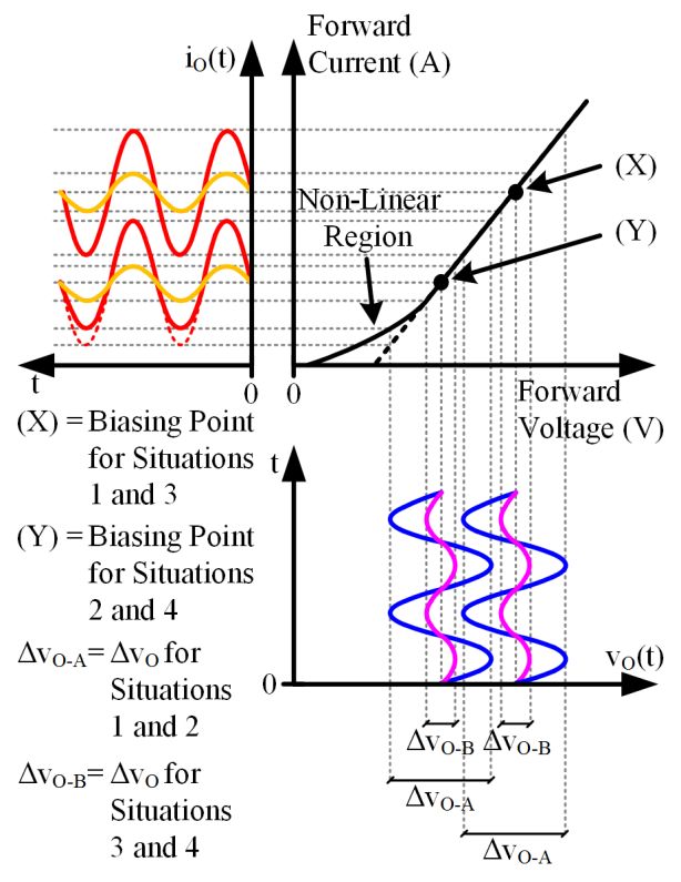
approaches are described in Section III. The experimental
results are given in Section IV and finally, the conclusions are 1
 = ( − · ( )) > · ( ). (2)
 ·
gathered in Section V.
 Considering the previous facts, the desired features of the HB-
 II. DRIVING HB-LEDS FOR PERFORMING VLC
 LED driver based on the use of DC-DC converters can be
 The VLC transmitter must be able to generate a light intensity stated:
waveform (sO) made up of a DC component (sO-DC) that Capability to reproduce a fast current reference. In order to
determines the lighting level, and an AC component (sO-AC) that maximize the bit rate, the HB-LED driver must exploit all the
represents the transmitted information. The study of the bandwidth provided by the HB-LEDs. Consequently, the
relationship between sO, the current through the HB-LED string HB-LED driver must be based on the use of a fast-response
(iO) and the applied voltage (vO) is essential to properly design DC-DC power converter able to reproduce current waveforms
the HB-LED driver. The behavior depends on the particular of several MHz.
HB-LED that is used, but certain general characteristics can be High output voltage accuracy. As Fig. 4 shows, the current
identified. Fig. 4 shows the main waveforms involved in the through the HB-LEDs does not start until the applied voltage
process of performing VLC with a HB-LED string considering overcomes n·VK. After that, a small increase of the voltage is
both the light intensity versus current (L-I) curve and the current translated into a high increase of the current and, consequently,
versus voltage (I-V) curve. Note that n represents the number a high increase of the light intensity. Then, the HB-LED driver
of HB-LEDs in series connection. It is assumed a linear must be able to perform very small voltage variations in
relationship between light intensity and current when the last comparison to the DC voltage that it must provide. In addition,
one is lower than a certain limit value (I Lim). Then, the it must minimize the output voltage ripple to reduce signal
relationship in the desired operation region (i.e., the linear distortion.
region) can be modeled as: Temperature compensation. As was previously explained, the
 relation between sO, iO and vO strongly depends on TJ.
 = · − · < , (1) Therefore, implementing some kind of current feedback loop is
 mandatory to ensure the proper reproduction of the target light
where KL-I is the proportionality coefficient of each HB-LED. intensity waveform.
Regarding the I-V curve, the behavior of a single HB-LED has Low/medium power. The power that the HB-LED driver must
been traditionally modeled as an ideal diode (D) in series with deliver strongly depends on the application scenario. For
the dynamic resistance (RD) and a constant voltage source that instance, the power of a HB-LED bulb for office environments
represents the knee voltage (VK). Fig. 4 also shows the is in the order of tens of watts, whereas it can attain thousands
dependence of the voltage waveform on the junction of watts in the case of a football stadium.
temperature of the HB-LEDs (TJ). Basically, VK falls when TJ High efficiency. Low power dissipation in the HB-LED driver
rises while RD remains constant [41]-[43]. Consequently, is essential to extend the use of VLC for providing services such
ensuring a certain voltage level does not guarantee the desired as Internet connection. In this sense, a 90% efficiency target
lighting level. Taking into account all these facts, the seems to be reasonable.
relationship between current and voltage in the desired Dimming capability. This last feature is recommended, but
operation region (i.e., the linear region) can be modeled as: not mandatory.

Fig. 4. Driving a string of n HB-LEDs in series connection for performing VLC by considering the L-I and I-V curves.
III. PROPOSED HB-LED DRIVER FOR REPRODUCING attention to VK and the voltage that determines I Lim (VLim).
 ADVANCED MODULATION SCHEMES Taking into account these two voltages, the maximum variation
 In order to support the explanation of the VLC transmitter of vO can be defined as:
presented in this work and to highlight its advantages, the ideas
contemplated by the authors before achieving the definitive = · [ ( ) − ( )]. (3)
approach are explained below.
 The high output voltage accuracy required by this approach
A. Controlling the Whole Current through the HB-LEDs
 arises when the ratio between ΔvO and the vO-DC is evaluated.
 Since the relation between vO and sO strongly depends on TJ, For instance, if the target iO-DC is 0.5·ILim, vO-DC is equal to:
the straightforward approach to implement the VLC transmitter
consists in controlling iO (see Fig. 5). In this way, the DC-DC − = · ( ) + 0.5 · . (4)
power converter drives the HB-LEDs with a current
proportional to the desired light intensity waveform according
 Then, the ratio is equal to:
to (1).
 The light intensity reference (sO-Ref) is made up of the lighting
 2 · [ ( ) − ( )]
level reference (sO-DC-Ref) and the communication component = . (5)
reference (sO-AC-Ref). Then, the current reference (iO-Ref) is − ( ) + ( )
obtained according to (1) and, after that, iO-Ref is compared to iO.
The result is processed by the Error Amplifier (EA) and, finally, Typically, VK and VLim are around 3 V and 3.5 V when T J is
the Pulse-Width Modulation (PWM) block generates the gate 25 ºC, respectively, which is translated into a very low ratio
signal of the MOSFETs according to the received control action (i.e., 1/6.5). In summary, the HB-LED driver must be able to
(i.e., the duty cycle d). perform very small voltage variations in comparison to the DC
 The simplicity constitutes the major advantage of this voltage that it must provide. Consequently, the DC-DC
approach. Unfortunately, the high switching frequency (f SW) converter must achieve high duty cycle accuracy.
required for implementing this method is a significant problem. B. Controlling the Average Current through the HB-LEDs
Take into account that fSW must be high enough to ensure a
 As previously mentioned, the impact of the feedback loop on
bandwidth equal or higher than the maximum frequency of s O
 the converter bandwidth leads to an unaffordable fSW when iO is
(fS-Max). The ideal minimum value of fSW is twice fS-Max
 controlled. Fortunately, this drawback can be overcome by
according to the Nyquist-Shannon sampling theorem. However,
 analyzing in detail how TJ affects the HB-LED behavior. As
this limit rises when the reactive elements of the power stage
 explained in Section II, VK falls when TJ rises while RD remains
and the dynamics related to the current feedback loop, such as
 constant. The key point is to study how the voltage waveform
the EA response, are considered. Therefore, fSW would be much
 required for tracking a certain sO changes with TJ. In this sense,
higher than fS-Max in practice. The key point is that since fS-Max
 Fig. 4 exemplifies this fact considering two particular T J values.
is in the order of MHz, fSW would be extremely high, which will
 It can be seen that the DC component of vO (i.e., vO-DC) depends
be translated into unaffordable switching losses.
 on TJ because of the change of VK. However, since RD does not
 Another drawback is the high output voltage accuracy
 depend on TJ, the AC component of vO (i.e., vO-AC) does not
required for reproducing sO-AC properly. It can be easily
 change. As a conclusion, a current loop is actually needed, but
understood with an example based on the I-V curve depicted in
 controlling the average current through the HB-LEDs (i.e.,
Fig. 4. Consider a string of n HB-LEDs acting as load and pay
 iO-DC) instead of the whole current waveform is enough for
 ensuring the proper operation. Thus, the feedback loop does not
 limit the speed of the HB-LED driver for reproducing the AC
 component of the current through the HB-LED string (i.e.,
 iO-AC). Therefore, the required fSW can be reduced in comparison
 to the approach described in Section III.A.
 Taking into account the previous considerations, a VLC
 transmitter based on a DC-DC converter that controls iO-DC
 instead of iO can be addressed (see Fig. 6). In this case, the
 output current is sensed and filtered to measure iO-DC. Since this
 value determines the lighting level, the DC component of the
 output current reference (iO-DC-Ref) is obtained from sO-DC-Ref by
 using (1) and, then, iO-DC-Ref is compared to iO-DC. Thus, the EA
 provides a constant control action (dDC) that ensures the desired
 lighting level. After that, the AC component of the control
 action (dAC), which is responsible for the communication signal,
 is added. At this point, the function that models the relationship
 between light intensity changes and duty cycle changes when
Fig. 5. HB-LED driver approach based on controlling iO.
C. Controlling the Average Current through the HB-LEDs
 and Splitting the Power
 The definitive approach is focused on both increasing the
 power efficiency and reducing the demanded duty cycle
 accuracy. The proposed HB-LED driver is made up of two
 DC-DC power converters in output-series connection (see Fig.
 7) and each one is designed to meet different objectives. The
 Low-Side Converter (LSC) operates in close-loop controlling
 iO-DC. Regarding the High-Sider Converter (HSC), it operates in
 open-loop performing the small voltage variations. The set of
 DC-DC converters works in the following way. The HSC
 provides vO-AC (i.e., the voltage component responsible for the
 communication) plus a certain DC voltage (vO-H-DC) required for
 the proper operation of the DC-DC converter. Note that vO-H-DC
 is mandatory to ensure that the total output voltage of the HSC
 (vO-H) never reaches zero or negative values (i.e., vO-AC + vO-H-DC
 > 0 V). The remaining DC voltage that is required for achieving
 the desired lighting level is provided by the LSC. Therefore, the
 LSC controls iO-DC by adjusting its output voltage (vO-L) to
 ensure that the total DC output voltage of the HB-LED driver
Fig. 6. HB-LED driver approach based on controlling iO-DC.
 (i.e., vO-DC = vO-L + vO-H-DC) achieves the desired biasing point
 regardless vO-H-DC and the VK variations with TJ. Then, the total
the HB-LED string operates in the linear region (fd-s) must be
obtained. This function allows us to calculate d AC from sO-AC-Ref.
Then, the L-I curve and the I-V curve must be considered in
order to obtain fd-s. Equation (1) is valid to obtain the
relationship between light intensity changes and current
changes. The relationship between current changes and voltage
changes can be deduced from (2):

 − = · · − . (6)

 Finally, the relationship between the output voltage and the
duty cycle must be used. Then, fd-s depends on the particular
DC-DC converter topology selected for the implementation.
For instance, if the approach is implemented with a buck
converter, the function is equal to:

 − ( − − ) = , (7)
 − · − −

where VG is the input voltage of the DC-DC converter. It is
important to note that the low-pass filter of the feedback loop
must reject the frequency components of iO related to the
communication signal in order to achieve the proper operation.
This enables the sum of dAC without interfering with the EA
operation.
 This method avoids the bandwidth limitation caused by the
feedback loop. Therefore, the bandwidth of the DC-DC
converter is only limited by the reactive elements of the power
stage, alleviating the main problem of the previous approach.
However, the required fSW keeps being significantly high and,
consequently, the HB-LED driver will suffer from high
switching losses when the highest data rates (i.e., highest f S-Max
values) are addressed. In addition, the required duty cycle
accuracy keeps being a problem. Fig. 7. HB-LED driver approach based on controlling i O-DC and splitting the
 power.
output voltage of the HB-LED driver is: respectively (see Fig. 8). The multi-phase buck topology [44]
 was conceived to be used as Voltage Regulator Modules
 = − + − = (VRMs) for supplying microprocessors due to the high
 = − + − − + − − = (8) efficiency and bandwidth achieved [45]-[46]. In addition, this
 = − + − − . topology is widely used as envelope amplifier when the
 Envelope Tracking (ET) technique is used to increase the
 It should be noted that fd-v (see Fig. 7) models the relationship efficiency of a RF Power Amplifier (RFPA) [47]-[54]. These
between the duty cycle of the HSC (dH) and vO-H. Then, this applications have some similarities with the HSC of the
function depends on the particular DC-DC converter topology proposed VLC transmitter architecture: the output voltage level
selected for the HSC implementation. As Fig. 7 shows, fd-v is is low, the demanding bandwidth is very high, very low output
used to obtain the DC component of the HSC duty cycle (dH-DC). voltage ripple is mandatory and in the case of both ET and VLC,
The AC component of the HSC duty cycle (dH-AC) can be a certain voltage reference must be tracked. It is important to
calculated using fd-s. As in the previous approach, this function note that a Mth order low-pass filter is considered at the output
depends on the particular DC-DC converter topology. of the P-phase buck converter. The use of a fourth or higher
 The HSC is the only DC-DC converter that must ensure a order output filter was already proposed in ET for reducing the
bandwidth equal or higher than fS-Max. As a result, its switching output voltage ripple [51]-[59].
frequency (fSW-H) is high. Theoretically, the required fSW-H is It is well known that driving floating MOSFET is difficult
equal to the required fSW of the approach described in Section when fSW is high. This problem appears in the conventional P-
III.B because, as in that case, the feedback loop does not limit phase buck converter, where the MOSFETs source terminals
the converter bandwidth. Therefore, the lowest fSW-H value that are connected to non-constant voltage points. However, in the
can be used is determined only by the reactive elements of the proposed configuration, the MOSFETs source terminals are
power stage. If a very fast topology is used, fSW-H can be reduced connected to the input voltage source negative terminal of the
to a value that ranges between 3 and 6 times the fS-Max value. As HSC (see Fig. 8). Thus, the MOSFETs driving task becomes
in the previous approach, the HSC will suffer from high easier if VG-H is used to supply the MOSFETs drivers of the
switching losses when the data rate requirement demands a HSC. Note that the position of the other HSC elements should
communication signal with high bandwidth and, as a be modified in order to properly perform the buck converter
consequence, a high fSW-H. However, the key point is that since
the HSC only delivers the part of the power determined by the
communication signal, which is significantly lower than the
total power, the impact of those switching losses in the overall
efficiency is mitigated. The rest of the power is delivered by the
LSC, which can achieve high efficiency because the selection
of its switching frequency (fSW-L) is not subject to a high
bandwidth requirement. Therefore, fSW-L can be significantly
lower than fSW-H. Note that since the LSC only needs to track a
constant current reference (iO-DC-Ref), its design and efficiency
are similar to those of a conventional HB-LED driver for
lighting applications. In practice, the LSC will typically operate
with fSW-L in the range of hundreds of kHz while the HSC will
operate with fSW-H in the MHz range. In summary, the power
delivered by the HSC must be minimized in order to maximize
the overall efficiency. It can be performed by selecting vO-H-DC
barely higher than the one that always ensures vO-H > 0 V.
 Another advantage of this approach is that the output-series
connection enables an accurate reproduction of vO-AC with
relative ease. Since the HSC is focused on performing the small
voltage variations while the LSC provides most of vO-DC, the
required duty cycle accuracy for each converter is not as critical
as in the previous approaches.
 Regarding the drawbacks, the two isolated input voltages
required for the implementation (i.e., VG-H and VG-L) is the
weakest point of the approach.
D. Selected DC-DC Converter Topologies
 In this paper, a multi-phase asynchronous buck converter
with P phases (P-phase buck converter) and a single-phase Fig. 8. HB-LED driver made up of a P-phase buck converter with a Mth order
 low-pass filter (HSC) and a single-phase synchronous buck converter with
synchronous buck converter are considered as HSC and LSC, second order low-pass filter (LSC).
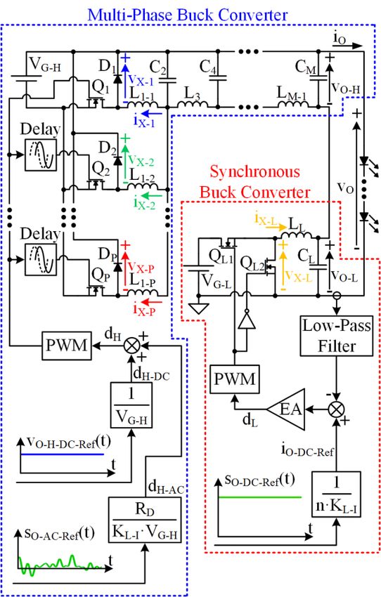
function.
 Regarding the LSC, its requirements are less challenging
than in the case of the HSC because it operates similarly to a
conventional HB-LED driver for lighting applications. In this
sense, a single-phase synchronous buck converter with second
order low-pass filter provides all the characteristics required to
fulfill the LSC target. As major advantages of this topology, the
power stage is made up of few elements, it achieves high
efficiency and its averaged model is very simple.
E. Steady State Operation
 Fig. 9(a) shows the equivalent circuit of the proposed (a)
HB-LED driver modeling vX-1, vX-2, …, vX-P (i.e., the
switch-node voltages of the HSC) and vX-L (i.e., the switch-node
voltage of the LSC) as ideal pulse voltage sources. Note that
this assumption is valid when the HSC operates in Continuous
Conduction Mode (CCM). In the case of the P-phase buck
converter (i.e., the HSC), there are P switch-node voltages (i.e.,
vX-1, vX-2, …, vX-P) and each one has a particular delay (i.e., td-1,
td-2,…, td-P) with respect to the switch-node voltage of the first
phase (i.e., vX-1). Then, each ideal pulse voltage source can be
modeled as:
 (b)
 − ( ) = −1 ( − − ). (9) Fig. 9. Equivalent circuits of the proposed HB-LED driver: (a) Modeling vX-1,
 vX-2, …, vX-P and vX-L as ideal pulse voltage sources. (b) Applying the
 Using a suitable delay pattern leads to a reduction of the superposition and the Thevenin’s theorems.
output voltage ripple. In this way, the benefit of the P-phase voltage ripple of the LSC in order to minimize the distortion of
structure arises when the delay pattern defined below is used: the reproduced signal.
 The reduction of the output voltage ripple achieved by the P-
 ( − 1) · − phase buck converter can also be understood from the main
 − = , (10)
 current waveforms. As Fig. 11 shows, the current delivered by
 each converter are identical (i.e., equal to iO) due to the output-
where TSW-H is the switching period of the HSC. series connection. Moreover, it is very important to analyze the
 In order to show the output voltage ripple reduction achieved current of each HSC phase (i.e., iX-1, iX-2, …, iX-P) in order to
by the P-phase structure, the superposition and the Thevenin’s understand the reduction of the output voltage ripple achieved
theorems are applied to obtain the schematic depicted in Fig. by the P-phase structure. Assuming that all phase inductances
9(b). Note that it is assumed that L1-1, L1-2, …, L1-P are identical are identical, the current ripple of each HSC phase will be equal.
and, consequently, L1 is equal to L1-1/P. In this way, an In addition, the DC component of the each phase current is i O/P
equivalent voltage source at the input of the equivalent HSC if the Equivalent Series Resistances (ESRs) of all phase
filter can be defined as: inductors are identical. Then, the inductor current of the ith
 phase is delayed td-i with respect to the inductor current of the

 1 1 first phase (see Fig. 11). As a result, the sum of all phase
 ( ) = ∑ − ( ) = ∑ −1 ( − − ). (11) currents (i.e., iT = iX-1 + iX-2 + … + iX-P) has lower ripple than in

 =1 =1 the case of a single phase.

 Fig. 10 shows the main voltage waveforms of the proposed F. Frequency Domain Analysis
HB-LED driver assuming steady state conditions. Note that The steady state analysis is a suitable initial step to study the
TSW-L is the switching period of the LSC. It can be seen that that general operating principle of the proposed HB-LED driver.
due to the delay pattern indicated in (10), vT has lower harmonic However, the frequency domain analysis must be carried out in
content than the switch-node voltages and, moreover, it is order to deeply understand the P-phase buck converter
placed at higher frequencies. Thus, the filtering task is easier operation, the synchronous buck converter operation and their
than in the case of a single-phase approach. joint operation as a single HB-LED driver.
 Another important point is that, as Fig. 10 shows, the total As previously explained, the P-phase buck converter is
output voltage ripple is made up of the output voltage ripple of responsible for reproducing the communication signal with
both converters (i.e., the P-phase buck converter and the high accuracy. The operating principle is based on providing
synchronous buck converter). Then, it is essential to reduce not the desired vO-AC from vX-1 [see Fig. 12(a)] by carefully filtering
only the output voltage ripple of the HSC, but also the output this pulse-width modulated voltage. Therefore, the transfer
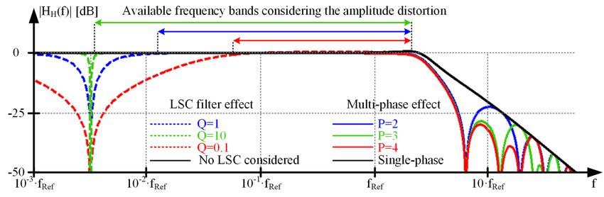
Fig. 11. Main current waveforms of the proposed HB-LED driver assuming
 steady state conditions.

 (a)

 (b)
 Fig. 12. Analysis of the relationship between the pulse-width modulated
 voltage at the first switch-node of the P-phase buck converter (i.e., vX-1) and
 vO-H: (a) Time domain analysis. (b) Frequency domain analysis.

Fig. 10. Main voltage waveforms of the proposed HB-LED driver assuming scheme that is being reproduced). Secondly, the phase-shift of
steady state conditions. HH(f) must be linear with frequency in those regions, ensuring
 a constant group delay.
function between vX-1 and vO [i.e., HH(f) = vO(f)/vX-1(f)] must be HH(f) will show the effect of the P-phase structure, the effect
analyzed. It is important to note that HH(f) must reject the of Mth order low-pass filter and the impact of the synchronous
switching harmonics together with their sidebands [see Fig. buck converter on the P-phase buck converter:
12(b)]. Moreover, this transfer function must meet some
additional requirements in order to avoid distortion when ( ) = − ( ) · − ( ) · − ( ), (12)
reproducing the signal reference. Firstly, its magnitude must be
flat in the desired frequency bands. Note that these frequency where HH-P(f) is the transfer function between vX-1 and vT (i.e.,
bands include the DC component and the frequency the effect of P-phase structure), HH-F(f) is the transfer function
components that appear due to the duty cycle variation over between vT and vO-H (i.e., the effect of Mth order low-pass filter),
time (i.e., the frequency components related to the modulation and HH-L(f) is the transfer function between vO-H and vO (i.e., the
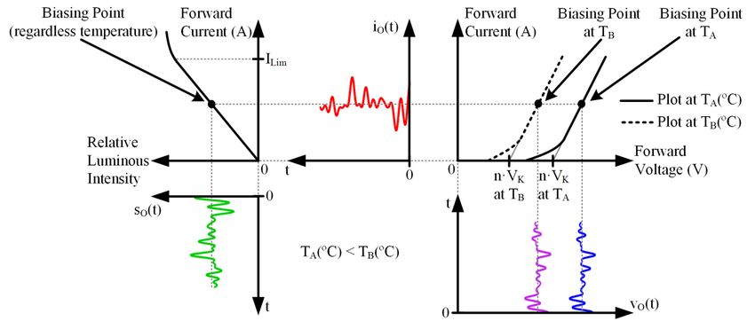
Fig. 13. Equivalent circuit of the proposed HB-LED driver that can be used to
obtain HH(f).

impact of the synchronous buck converter). The equivalent
circuit depicted in Fig. 13 can be used to analyze HH(f).
 Starting with the Mth order low-pass filter, it is well-known (a)
that it causes a magnitude drop for frequencies higher than the
cut-off frequency (fC-H). Therefore, fC-H must be higher than the
highest frequency component of the signal (i.e., fS-Max). There is
an important trade-off between fC-H, fSW-H, fS-Max and the order
of the filter. fC-H must be high enough to not distort the
frequency components of the signal and, at the same time, it
must be low enough to ensure enough rejection of the switching
harmonics and their sidebands. In order to alleviate this
problem, fSW-H can be increased in exchange for higher
switching losses. Another option consists in increasing the filter
order. However, this is translated into higher complexity and (b)
cost. This issue has been deeply studied in [51] and [57] for the Fig. 14. HH-P(f) analysis: (a) Magnitude. (b) Phase.
ET application, and the design guidelines included in these
works are valid for the P-phase buck converter of the proposed
HB-LED driver. As in [51] and [57], the source impedance of
the filter is 0 Ω and, consequently, proper filter tables must be
used. In this case, n·RD must be considered as the load
impedance of the filter.
 Regarding HH-P(f) and according to (9), (10) and (11), it can
be defined as:

 ( )
 − ( ) = =
 −1 ( )
 1 sin( · · − ) − · · · − ·( −1) (13)
 = . (a)
 sin ( · · − )

 Then, the multi-phase structure introduces notch filters at
some switching frequency harmonics, contributing to reduce
the output voltage ripple. As Fig. 14 shows, the higher the
number of phases, the higher the number of notch filters and the
lower the output voltage ripple.
 Regarding the impact of the synchronous buck converter on
the P-phase buck converter, the output filter of the LSC also
introduces a notch filter at its cut-off frequency (fC-L). Fig. 15
shows HH-L(f) for different Q values of the synchronous buck (b)
converter filter keeping the same fC-L. Note that the expression Fig. 15. HH-L(f) analysis: (a) Magnitude. (b) Phase.
utilized for the Q factor evaluation is:
 different LSC filter designs that keep the same fC-L but change
 the Q factor. It is important to note that fRef represents the
 central frequency of the modulation scheme that is going to be
 = · · √ . (14)
 reproduced. The rest of signal components would be placed
 around fRef. It can be seen that the available frequency band for
 Finally, Fig. 16(a) shows |HH(f)| highlighting the different the communication signal depends on the Q factor of the LSC
effects. This figure considers different number of phases and filter. Note that in Fig. 16(a), the identification of the available
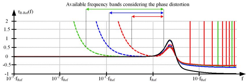
(a)

 (b)
Fig. 16. HH(f) analysis: (a) Magnitude. (b) Relative variation of the group delay with respect to the group delay at f Ref.

frequency band only considers the amplitude distortion.
However, the phase distortion also plays an important role [see
Fig. 16(b)]. Therefore, the relative variation of the group delay
with respect to the group delay at f Ref [i.e., τR-Ref(f)] must be
evaluated:

 [ ( ) − ( )]
 − ( ) = , (15)
 ( )

where τ(f) is the group delay of HH(f). The actual available
frequency band is the smallest of both approaches (i.e.,
considering the amplitude and the phase distortion) and it
depends on the limits employed to identify the bands. In other Fig. 17. Equivalent circuit of the proposed HB-LED driver that can be used to
words, the maximum attenuation permitted in the case of the obtain GdL-i(f).
amplitude distortion, and the maximum relative variation of the
 Fig. 18 shows GdL-i(f) for different Q values of the
group delay permitted in the case of the phase distortion. In any
 synchronous buck converter filter, highlighting the impact of
case, it can be concluded that a high Q factor is desirable for
 the P-phase buck converter. It can be seen that the output
maximizing the available frequency band. Moreover, fC-L must
 impedance of the HSC introduces certain notch filters at high
be placed between the DC component and the lowest harmonic
 frequencies. Fortunately, this fact has minor impact on the
of the reproduced modulation scheme.
 current feedback loop and, consequently, the synchronous buck
 Regarding the synchronous buck converter, how it is affected
 converter can be designed similarly to a conventional HB-LED
by the P-phase buck converter when it tries to control iO must
 driver for lighting applications. It is important to note that the
be analyzed. There are several transfer functions that can be
 low-pass filter of the feedback loop must be taken into account
calculated in order to address this point. In this paper, the
 for designing the regulator. The cut-off frequency of this low-
transfer function between the duty cycle (i.e., d L) and iO
 pass filter should be as low as possible but, at the same time,
[GdL-i(f)] is obtained and studied by using the equivalent circuit
 high enough to not jeopardize excessively the bandwidth of the
depicted in Fig. 17.
 feedback loop. In general, this point is not an issue and, in
the VG-H value, the lower the duty cycle accuracy required to
 generate vO-H and, as a consequence, the lower the demanded
 time resolution of the Field Programmable Gate Array (FPGA).
 Therefore, it is essential to determine the minimum VG-H value
 (VG-H-Min) that could to be used. The duty cycle of the P-phase
 buck converter (i.e., dH) must be always lower than a maximum
 value (dH-Max) and higher than a minimum value (dH-Min) that are
 stablished due to safety reasons. For the sake of simplicity, the
 same safety margin is considered for both duty cycle limits (i.e.,
 dH-Min = 1 - dH-Max). Note that Fig. 19 can be used to understand
 the reasoning related to Step 3. Under the aforementioned
 considerations and when the converter operates with the
 maximum communication power, the following equation can
 (a) be used to determine VG-H-Min:

 · − − = · − − + − . (16)

 Therefore, VG-H must satisfy the following condition:

 −
 − ≥ − − = . (17)
 1 − 2 ·

 It is important to note that vO-H-DC is defined as:

 (b) − − = · − + . (18)
Fig. 18. GdL-i(f) analysis: (a) Magnitude. (b) Phase. 2
practice, a cut-off-frequency similar to fC-L fulfills the As a result, the following condition is always satisfied:
application requirements.
G. Design Guidelines − ≥ · − > 0 . (19)
 The recommended steps for the design of the proposed VLC
 The maximum value of vO-H-DC is reached when the
transmitter are described in this section. The design
 communication power is the highest one:
specifications should include the maximum lighting level (sO-
DC-Max) and the modulation scheme that must be reproduced
 − − − = 0.5 · − − . (20)
together with the maximum power of the communication
signal, thus defining sO-AC for the highest communication
power. It is important to note that the modulation scheme does
not determine the communication signal power because it only
determines the shape of the signal. The same signal can be
transmitted with different power levels (i.e., more or less
amplification) depending on the particular application
requirements.
 Step 1: dimensioning the HB-LED string. The number of HB-
LEDs of the string (i.e., n) can be calculated by taking into
account sO-DC-Max, the dynamic resistance (i.e., RD) and the knee (a)
voltage (i.e., VK) of the HB-LEDs selected for the
implementation.
 Step 2: characterization of iO-AC and vO-AC for the highest
communication power. iO-AC and vO-AC for the highest
communication power (iO-AC-Max and vO-AC-Max, respectively) can
be obtained by considering (1), (2) and the equivalent dynamic
resistance of the HB-LED string selected in Step 1 (i.e., n·RD).
After that, the peak to peak value of vO (ΔvO) for the highest
communication power (ΔvO-Max) can be calculated from vO-AC-
Max.
 (b)
 Step 3: determining VG-H. It is important to note that the lower Fig. 19. vO-H for two communication power levels using VG-H = VG-H-Min: (a)
 Maximum communication power. (b) Lower communication power.
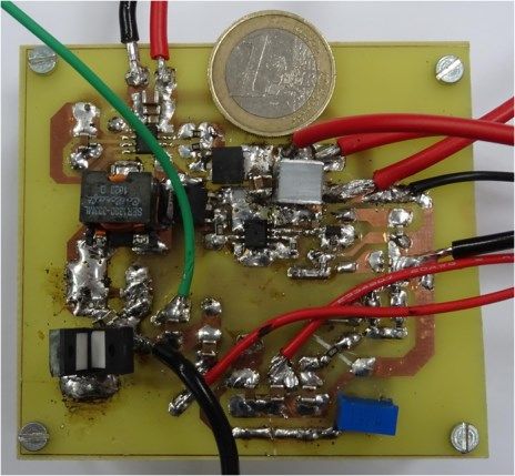
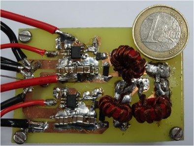
Step 4: Selecting the number of phases (i.e., P) and the order scheme that is made up of 29 carriers is reproduced. It is
of the filter (i.e., M). As is explained in Section III.F, both the important to note that the maximum frequency component of
multi-phase effect and the high order output filter contribute to the reproduced modulation scheme (i.e., fS-Max) is around 3
reduce the output voltage ripple. Therefore, both points must be MHz. The sequence of duty cycle values that the HSC requires
addressed together. Obviously, the higher the number of phases, to reproduce the communication signal (i.e., dH) is stored in the
the lower the required order of the filter and vice versa. As a FPGA that controls the two-phase buck converter.
consequence, there are several solutions (i.e., several
combinations of P and M) that, showing similar complexity
(which could be evaluated using P + M), ensure a certain level
of output voltage ripple rejection. In order to select the most
appropriate solution for the particular requirements of the VLC
transmitter, parameters that are difficult to be measured, such
as the dependence of the cost or of the size on P and M, must
be taken into account. In any case, it is recommendable to
follow the directions of [51] and [57] for determining M and the
cut-off frequency of the filter (i.e., fC-H) once P is selected.
 Step 5: Designing the synchronous buck converter. In the
case of the synchronous buck converter, the input voltage (i.e.,
VG-L) can be selected according to standard voltage values such
as 24 V or 48 V. As is explained in section III. F, the cut-off
frequency of the filter (i.e., fC-L) should be lower than the
minimum frequency of the communication signal that the P-
phase buck converter is going to reproduce. In addition, the Q (a)
value of the filter should be high enough to avoid the distortion
of the communication signal. The design of the feedback loop
is straightforward.

 IV. EXPERIMENTAL RESULTS
A. Prototype Details
 A two-phase asynchronous buck converter and a single-
phase synchronous buck converter were built to test
experimentally the proposed HB-LED driver (see Fig. 20). The (b)
switching frequency of the two-phase buck converter and the
synchronous buck converter is 10 MHz and 250 kHz,
respectively. The output filter of the HSC is a 4 th order
Butterworth filter with a cut-off frequency equal to 4 MHz. In
the case of the LSC, the cut-off frequency of the 2nd order filter
is 20.5 kHz and the Q value is 1.56. Table I shows the passive
components used for the filters implementation. The inductors
of the HSC are implemented with iron powder cores (T50-2)
from Micrometals. A SER1390-333MLB inductor from
Coilcraft is used for the inductor of the LSC. The low-pass filter
of the feedback loop is implemented with a RC filter whose cut-
off frequency is 15.9 kHz. Silicon MOSFETs are used in both
converters: SSM3K336R in the two-phase buck converter and (c)
TK7S10N1Z in the synchronous buck converter. In both cases, Fig. 20. Two-phase buck converter with 4th order Butterworth filter in
the MOSFETs are driven by EL7156 ICs. Schottky diodes output-series connection with a synchronous buck converter: (a) Schematic
DB2430500L are used in the HSC. The load is made up of 6 circuit of the implemented HB-LED driver. (b) Two-phase buck converter
 prototype. (c) Synchronous buck converter prototype.
HB-LEDs (W42180 Seoul Semiconductor) connected in series.
The input voltage of the two-phase buck converter and the
synchronous buck converter is 8.5 V and 24 V, respectively. TABLE I. PASSIVE COMPONENTS USED FOR THE OUTPUT FILTERS
 IMPLEMENTATIONS.
PDA10A-EC is used as the receiver of the VLC setup. Since
this device is made up of a photodiode and a transconductance L1-1 L1-2 C2 L3 C4 LL CL
amplifier, its output signal is a voltage waveform proportional Component (nH) (nH) (nF) (nH) (nF) (μH) (μF)
to the received light intensity.
 Value 812 812 9.4 287.1 2.3 33 1.818
 Regarding the communication signal, a 64-QAM-OFDM
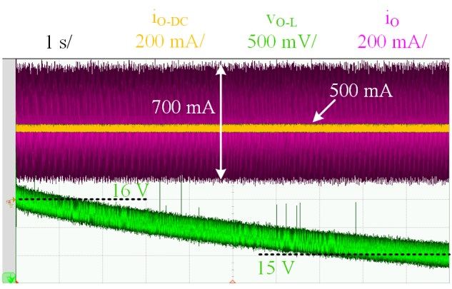
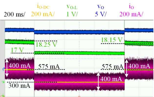
B. Evaluation of the Trade-Off between Communication
Efficiency and Power Efficiency
 In order to deeply evaluate the performance of the HB-LED
driver prototype, it is tested under different operating
conditions. The test target is to study how the lighting level and
the communication signal power affect both the power
efficiency and the communication efficiency. Obviously, the
lighting level depends on the average current through the HB-
LED string (i.e., iO-DC). Regarding the communication signal
power, it can be controlled by adjusting the peak to peak value
of vO (i.e., ΔvO).
 Two lighting levels (determined by iO-DC = 300 mA and iO-DC
= 500 mA) and two levels of the communication signal power
(determined by ΔvO = 4.1 V and ΔvO = 2.2 V) are considered.
As a result, there are four possible situations (see Table II). It is
important to note that the distance between the transmitter and
the receiver is 20 cm in all situations. Fig. 21 exemplifies the
performed test and facilitates the understanding of the
reasoning that will appear along this section.
 Fig. 22 shows the main waveforms of the VLC system for
each situation. Note that vRX is the receiver signal. The DC
component of vRX (vRX-DC) measures the lighting level while the
peak to peak value (ΔvRX) is determined by the received
communication signal power. Table II indicates both the DC
component and the peak to peak value of each waveform. Note
 Fig. 21. Graphical description of the test considering the I-V curve of the HB-
that ΔiO is the peak to peak value of iO. In addition, it shows the LED string and sinusoidal waveforms.
amount of power delivered by the two-phase buck converter
(PO-H) and by the synchronous buck converter (P O-L), the as in situation 1 and, consequently, the operating conditions of
efficiency of the two-phase buck converter (ηH), the efficiency the two-phase buck converter are almost the same. Actually,
of the synchronous buck converter (ηL), the overall efficiency ΔiO and ΔvRX slightly change because the transmitter partially
(η) and a figure-of-merit for evaluating the communication works in the non-linear region of the HB-LED string. It can be
efficiency that will be introduced below. easily understood seeing Fig. 21. How this fact affects the
 In situation 1, iO-DC and ΔvO-AC are 500 mA and 4.1 V, communication will be addressed below. Taking into account
respectively. Note that as indicated in Section II, vO-AC is small all these considerations, the weight of the synchronous buck
in comparison to vO-DC. It can be seen that most of vO-DC is efficiency on the overall efficiency is lower in situation 2 than
delivered by the synchronous buck converter. In this situation, in situation 1 and, consequently, the overall efficiency falls.
the power of the HB-LED driver is 10.1 W, the 81% of the In order to study the impact of reducing the communication
power is provided by the synchronous buck converter and the signal power on the power efficiency of the HB-LED driver,
overall efficiency is 91.3%. situation 3 can be compared to situation 1 (ΔvO falls from 4.1 V
 Comparing situation 2 to situation 1 allows us to study the to 2.2 V). All the peak to peak values of the waveforms change
impact of decreasing the lighting level on the power efficiency while the values of iO-DC, vO-DC and vRX-DC are the same as in
of the HB-LED driver (iO-DC falls from 500 mA to 300 mA). In situation 1. However, it is important to note that the output
order to achieve the lower biasing point, the synchronous buck voltage of the synchronous buck converter is higher in the case
converter decreases its output voltage and, as a result, the of situation 3. It is because the AC voltage provided by the two-
amount of power delivered by this converter falls. It is phase buck converter is lower in this situation, so its DC voltage
important to note that since the communication signal power is is reduced to minimize the power that it delivers. Consequently,
the same, the peak to peak values of the waveforms are the same the synchronous buck converter increases its output voltage to
TABLE II. MAIN PARAMETERS OF THE TEST PERFORMED TO EVALUATE THE TRADE-OFF BETWEEN COMMUNICATION EFFICIENCY AND POWER EFFICIENCY.

 iO-DC ΔiO vO-DC ΔvO vO-L vRX-DC ΔvRX PO-L PO-H PO ηL ηH η EVMRMS
 (mA) (mA) (V) (V) (V) (mV) (mV) (W) (W) (W) (%) (%) (%) (%)

 Situation 1 500 750 19.9 4.1 16.1 34 29 8.19 1.24 10.1 92.8 79.2 91.3 22.3

 Situation 2 300 575 19 4.1 15.2 23 25 4.64 1.23 5.87 89.7 84.5 88.6 27.6

 Situation 3 500 350 19.9 2.2 18.2 34 15 9.56 0.52 10.08 94.8 75.7 93.6 23.2

 Situation 4 300 300 19 2.2 17.3 23 15 5.31 0.51 5.82 92.4 81.3 91.3 24
achieve the desired lighting level. As Table II shows, the total
 power of the HB-LED driver is almost the same in situation 1
 and in situation 3, but the power share is different. It can be seen
 that in situation 3, the power provided by the synchronous buck
 converter (94.8% of the total power) is higher than in situation
 1 and, as a result, the overall efficiency rises.
 Finally, the remaining case appears in situation 4, where both
 the lighting level and the communication signal power fall (iO-
 DC falls from 500 mA to 300 mA and Δv O falls from 4.1 V to
 2.2 V). In this situation, the power of the HB-LED driver is 5.82
 W, the synchronous buck converter delivers the 91.2% of the
 total power and the overall efficiency is 91.3%.
 (a)
 Fig. 23 shows an estimation of the losses distributed in the
 components of the experimental prototype for each operating
 situation. It can be seen that although P O-H is much lower than
 PO-L in all operating situations (see Table II), the semiconductor
 switching losses of the two-phase buck converter is one of the
 major source of power losses.
 In summary, minimizing the communication signal power
 and maximizing the lighting level is the best strategy for
 achieving the highest power efficiency. This conclusion fits in
 with the converters efficiency because the strategy leads to
 minimize the power delivered by the HSC and to maximize the
 (b) power delivered by the LSC. In this way, the overall efficiency
 of the HB-LED driver is mainly determined by the LSC
 efficiency.
 However, the impact of both the lighting level and the
 communication signal power on the communication efficiency
 must also be evaluated to show a more general vision of the
 VLC transmitter performance. Basically, the communication
 efficiency depends on two parameters: the distortion and the
 power of the received signal. In general, the higher the power
 of the received signal, the higher the communication efficiency
 because the signal can be demodulated easier. Obviously, the
 (c) higher the signal distortion, the lower the communication
 efficiency.
 The error vector (e̅) is employed to measure the accuracy of
 the communications system:

 ̅ − ̅ ,
 ̅ = (21)

 where W̅ is the received symbol and V
 ̅ is the ideal symbol. Note
 that a symbol is a vector whose magnitude and direction are
 determined by the amplitude and the phase of a certain sinusoid.
 The modulation scheme defines the possible symbols (i.e., the
 (d) amplitude and phase combinations that the sinusoid can have)
Fig. 22. Main experimental waveforms of the VLC system during the test
performed to evaluate the trade-off between communication efficiency and and the bit sequence that univocally identify each one. In this
power efficiency: (a) Situation 1. (b) Situation 2. (c) Situation 3. (d) Situation way, the transmission of a particular symbol leads to the
4.

Fig. 23. Estimation of the power losses distribution in the components of the experimental VLC transmitter for each operating situation.
transmission of a particular bit sequence and, consequently, the
transmission of information. The reproduced 64-QAM-OFDM
scheme is made up of several carriers (i.e., sinusoidal
waveforms with different frequencies), and each one transmits
a symbol (i.e., each one has a particular amplitude and a
particular phase) during a certain time interval which is referred
as symbol period (T Sym). The e̅ calculation is used to evaluate
the performance of the communication system by evaluating
the Error Vector Magnitude (EVMRMS) [60]. This widely used
figure-of-merit evaluates e̅ for each carrier during a sequence of
several symbol periods considering the average power of the
involved symbols:

 2
 ∑
 =1 ∑ =1 |
 ̅̅̅̅̅|
 ,
 = √ , (22)
 ∑ ̅̅̅̅̅ 2
 =1 ∑ =1 | , |

where N is the number of symbols periods and C is the number Fig. 24. EVMRMS for different bit rates when the VLC system is evaluated in
of carriers. The lower the EVMRMS value, the higher the the laboratory setup and it operates in the situation 1.
communication efficiency. Typically, a value around 5%-15%
is required to fulfill the requirements of commercial wireless C. Bit Rate Evaluation
communication systems. Table II shows the EVMRMS value The reproduced 64-QAM-OFDM scheme is made up of 29
obtained in each situation. It can be seen that the measured carriers. The lowest carrier frequency and the highest carrier
values do not accomplish with the communication standards. frequency are 200 kHz and 3 MHz, respectively. Each carrier
However, as will be explained in Section IV.C, this issue can provides a bit rate equal to 600 kbps and, consequently, the
be solved by adjusting the communication speed to the maximum bit rate achieved by this modulation scheme is 17.4
particular communication scenario where the VLC system is Mbps. However, the speed of the communication signal must
evaluated. be evaluated together with EVMRMS in order to show a
 The best result is obtained when iO-DC is 500 mA and ΔvO is consistent result. It is important to note that, in general, the
4.1 V (i.e., situation 1). If the lighting level is considerably higher the communications speed, the higher the number of
reduced (i.e., the situation changes from 1 to 2), EVM RMS rises transmission errors. However, the actual values of these two
dramatically although the communication signal power is the parameters depend on the communication scenario, which, in
same. The reason is that the HB-LED string must be operating addition, changes over time. One of the advantages of OFDM
in the current-voltage linear region to properly reproduce the schemes is that the communication speed can be dynamically
communication signal. However, ΔvO is too high for the iO-DC adjusted to reduce EVMRMS. This is performed by deactivating
value considered in situation 2 (Fig. 21 may help to understand the carriers that are causing more transmission errors.
this phenomena). Thus, the HB-LEDs operate close to VK, Fig. 24 shows the measured relationship between EVMRMS
where the non-linear current-voltage relation causes high signal and bit rate when the VLC system is evaluated in the laboratory
distortion. Then, the communication signal power should be setup and it operates in situation 1. It can been seen that
reduced when considering the lighting level of situation 2 in EVMRMS is too high for the maximum speed. Therefore, for this
order to avoid the non-linear region. In this way, EVMRMS can particular communication scenario, a bit rate lower than 7.5
be improved by reducing ΔvO. It is equivalent to move from Mbps should be used to accomplish with most extended
situation 2 to situation 4. It can be seen that, as expected, communication standards (i.e., EVMRMS ≤ 15%).
EVMRMS is lower than in the case of situation 2 because it
reduces the distortion caused by the non-linear operation. D. Feedback Loop Tests
However, since the communication signal power is lower than Several tests have been carried out in order to check the
in the case of situation 1, EVMRMS is not as low as in that feedback loop behavior of the implemented HB-LED driver.
situation. Finally, EVMRMS can be reduced a bit by increasing Fig. 25(a) shows how the synchronous buck converter reduces
the lighting level (i.e., moving from situation 4 to situation 3) its output voltage in order to compensate the fall of V K with TJ.
in order to completely avoid the non-linear operation. Thus, both iO-DC and ΔiO remain constant over time. Note that
 As a conclusion, there is trade-off between power efficiency for this test, the HB-LEDs heat sink was removed to see a
and communication efficiency. For a particular lighting level, considerable change during a short period of time.
the communication signal power must be the maximum Fig. 25(b) shows the results when two changes in the
possible without operating in the non-linear region in order to communication signal power are performed. When the increase
maximize the communication efficiency. However, from the of the communication signal power occurs, the two-phase buck
power efficiency perspective, the best results are obtained when increases not only the AC component of its output voltage, but
the communication signal power is minimized. also the DC component. Remember that the DC component of
 the two-phase buck converter output voltage is adjusted to
 provide the minimum value that enables the reproduction of the
for reproducing waveforms of several MHz causes that
 conventional HB-LED drivers for lighting applications cannot
 be directly adopted.
 A HB-LED driver made up of a multi-phase buck converter
 with high order output filter in output-series connection with a
 synchronous buck converter is presented and deeply evaluated
 in this work. The multi-phase buck converter achieves high
 bandwidth operating in open-loop with high switching
 frequency. In this way, it is responsible for performing the small
 voltage variations (i.e., the communication signal component).
 On the other hand, the synchronous buck converter operates in
 close-loop ensuring that the desired lighting level is achieved.
 (a) The split of the power enables the maximization of the power
 efficiency by minimizing the power that the multi-phase buck
 converter must deliver in each possible communication
 scenario. Moreover, the output-series connection enables an
 accurate reproduction of the communication signal with relative
 ease.
 The joint operation of both converters is studied, focusing the
 attention on the multi-phase effect, the high order output filter
 effect and the impact of each converter on the other. It is
 concluded that the multi-phase structure supports the filtering
 task by reducing the output voltage ripple, whereas high Q
 factors of the synchronous buck converter filter are desirable
 for reducing the signal distortion. Moreover, the multi-phase
 (b)
 buck converter has minor impact on the synchronous buck
 operation and, consequently, its design is similar to
 conventional HB-LED drivers for lighting applications.
 The wide experimental section allows us to analyze the trade-
 off that exists between communication efficiency and power
 efficiency. The key point is that for a particular lighting level,
 the power efficiency falls when the communication signal
 power rises. However, from the communication perspective,
 the communication signal power must be the maximum
 possible without operating in the non-linear region.

 ACKNOWLEDGMENT
 (c) This work has been supported by the Spanish Government
Fig. 25. Main experimental waveforms of the VLC system during the feedback under the Project MINECO-17-DPI2016-75760-R, the
loop tests: (a) Compensation of the VK fall with TJ. (b) Response to two
changes of the communication signal power. (c) Response to two changes of
 scholarship FPU14/03268 and the Principality of Asturias
the lighting level. under the Project FC-15-GRUPIN14-143, the Project SV-PA-
 17-RIS3-4 and by European Regional Development Fund
AC component. As a consequence, the synchronous buck (ERDF) grants.
converter reduces its output voltage to compensate the change.
 Finally, Fig 25(c) shows the results when two changes in the
 REFERENCES
lighting level are performed. It can be seen how the
synchronous buck converter modifies its output voltage to track [1] Cisco Systems, “Cisco visual networking index: global mobile data
 traffic forecast update, 2016-2021”, Feb. 2017. [Online]. Available:
the desired lighting level. http://www.cisco.com/c/en/us/solutions/collateral/service-
 provider/visual-networking-index-vni/mobile-white-paper-c11-
 V. CONCLUSIONS 520862.html
 [2] “IEEE standard for local and metropolitan area networks--part 15.7:
 Although VLC is an application with high potential for short-range wireless optical communication using visible light," in IEEE
alleviating the congestion of the RF spectrum, it has some Std 802.15.7-2011, vol., no., pp.1-309, Sept. 6 2011.
bottlenecks that are slowing down its deployment. One of the [3] GBI Research, “Visible Light Communication (VLC)—a potential
most important problems is the low power efficiency of the HB- solution to the global wireless spectrum shortage”, Sep. 2011 [Online].
 Available: http://www.gbiresearch.com
LED drivers proposed for reproducing advanced modulation [4] H. Elgala, R. Mesleh, and H. Haas, “Indoor optical wireless
schemes. The use of DC-DC converters seems to be the solution communication: potential and state-of-the-art,” IEEE Commun. Mag.,
for solving the problem. However, the high bandwidth required vol. 49, no. 9, pp. 56–62, Sep. 2011.
You can also read