Recycling silver nanoparticle debris from laser ablation of silver nanowire in liquid media toward minimum material waste - Nature
←
→
Page content transcription
If your browser does not render page correctly, please read the page content below
www.nature.com/scientificreports
OPEN Recycling silver nanoparticle
debris from laser ablation
of silver nanowire in liquid media
toward minimum material waste
June Sik Hwang1, Jong‑Eun Park2, Gun Woo Kim3, Hyeono Nam2, Sangseok Yu4,
Jessie S. Jeon2, Sanha Kim2, Huseung Lee1* & Minyang Yang5*
As silver nanowires (Ag NWs) are usually manufactured by chemical synthesis, a patterning process
is needed to use them as functional devices. Pulsed laser ablation is a promising Ag NW patterning
process because it is a simple and inexpensive procedure. However, this process has a disadvantage in
that target materials are wasted owing to the subtractive nature of the process involving the removal
of unnecessary materials, and large quantities of raw materials are required. In this study, we report
a minimum-waste laser patterning process utilizing silver nanoparticle (Ag NP) debris obtained
through laser ablation of Ag NWs in liquid media. Since the generated Ag NPs can be used for several
applications, wastage of Ag NWs, which is inevitable in conventional laser patterning processes,
is dramatically reduced. In addition, electrophoretic deposition of the recycled Ag NPs onto non-
ablated Ag NWs allows easy fabrication of junction-enhanced Ag NWs from the deposited Ag NPs.
The unique advantage of this method lies in using recycled Ag NPs as building materials, eliminating
the additional cost of junction welding Ag NWs. These fabricated Ag NW substrates could be utilized
as transparent heaters and stretchable TCEs, thereby validating the effectiveness of the proposed
process.
Silver nanowire (Ag NW) percolation networks have attracted considerable attention as flexible and stretchable
transparent conductive electrode (TCE) materials because they have high electrical conductivity and higher
flexibility than indium tin oxide (ITO)1–3. These advantages have led to the development of various Ag NW-
based optoelectronic devices, such as touch screen sensors4,5, transparent heaters6,7, skin sensors8–10, organic
light-emitting diodes (OLEDs)11,12, and solar cells13,14. As the Ag NW layer is usually fabricated from a solution
process, patterning of the deposited Ag NW layer is performed for using this layer in practical applications. For
example, Shin et al. reported a capacitive touch screen sensor fabricated from a patterned Ag NW layer5 and Hong
et al. introduced a patterned Ag NW transparent heater for focused heating in specific regions7. Local thermal
insulation from patterned Ag NW cloth is also reported by Hus et al.9, and Won et al. discussed the improved
mechanical properties of electronic skin sensors obtained from a Kirigami-engineered pattern of Ag N Ws10. For
patterning Ag NWs, several methods have been introduced, including p hotolithography , printing17,18, laser
15,16
ablation19,20, and a transfer method21,22. Among the various patterning processes, pulsed laser ablation (PLA) of
Ag NWs is considered a promising patterning process because it involves a simple and inexpensive setup with-
out requiring the use of a mask or processes such as chemical etching or lithography. In particular, nanosecond
near-infrared PLA (NIR PLA) of Ag NWs has been studied e xtensively19,23–28 because of the relatively low-cost
source and little damage to the non-rigid substrate.
One of the major issues of the conventional laser patterning process, which is a subtractive process, is waste
generation as patterning is performed by material removal. In the patterning process through laser ablation, the
1
Department of Mechanical & Materials Engineering Education, Chungnam National University (CNU),
99 Daehak‑ro, Yuseong‑gu, Daejeon 34134, Republic of Korea. 2Department of Mechanical Engineering,
Korea Advanced Institute of Science and Technology (KAIST), 291 Daehak‑ro, Yuseong‑gu, Daejeon 34141,
Republic of Korea. 3Visual Display Business, Samsung Electronics, 129 Samsung‑ro, Yeongtong‑gu, Suwon‑si,
Gyeonggi‑do 16677, Republic of Korea. 4Department of Mechanical Engineering, Chungnam National University
(CNU), 99 Daehak‑ro, Yuseong‑gu, Daejeon 34134, Republic of Korea. 5Department of Mechanical Engineering,
The State University of New York, Korea (SUNY Korea), 119 Songdo Moonhwa‑ro, Yeonsu‑gu, Incheon 21985,
Republic of Korea. *email: liber@cnu.ac.kr; minyang.yang@sunykorea.ac.kr
Scientific Reports | (2021) 11:2262 | https://doi.org/10.1038/s41598-021-81692-9 1
Vol.:(0123456789)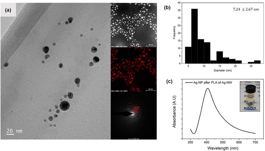
www.nature.com/scientificreports/
Figure 1. Schematic of the minimum-waste laser patterning process. (a) Pulsed laser ablation (PLA) of silver
nanowire (Ag NW) in liquid media. The inset presents the dispersion of Ag NP debris. (b) Electrophoretic
deposition (EPD) of silver nanoparticles (Ag NPs) on non-ablated Ag NWs. Inset shows the junction-enhanced
Ag NW from Ag NP deposition.
target material irradiated with high energy usually vaporizes or forms a plasma and disappears. As the patterned
region grows, the resulting waste also increases, and additional costs are incurred29. Furthermore, as the patterned
Ag NWs inherently have weak contact bonds, an additional junction welding process is often required to produce
high-performance Ag NW TCEs. With the requirement for additional equipment or materials, the advantages of
PLA, which are its simplicity and low cost, are easily lost. Therefore, there is a strong need for a laser patterning
process that generates less waste and involves simple and low-cost junction welding of the non-ablated Ag NWs.
Pulsed laser ablation in liquid (PLAL) is a simple process that generates nanoparticles from a bulk target
material30–32. When a focused laser beam is irradiated onto the target material, it experiences plasma formation,
followed by fragmentation due to the strong effects of cavitation bubbles. The condensed plumes split, thereby
generating NPs. Moreover, surface potentials are formed under the influence of the surrounding liquid media.
The resulting NPs can be deposited on conductive electrodes by electrophoretic deposition (EPD), thereby
forming metal nanostructures33–38.
In this study, we developed a minimum-waste laser patterning process utilizing silver nanoparticle (Ag NP)
debris through laser ablation of Ag NWs in liquid media. As the generated Ag NPs can be used for a variety of
applications, the fraction of Ag NWs discarded during the typical laser patterning process can be dramatically
reduced. Furthermore, from the EPD of the recycled Ag NPs onto unpatterned Ag NWs, enhanced junctions
of Ag NWs could be easily formed from the deposited Ag NPs. The unique advantage of this method is that
the recycled Ag NPs are used as building materials for fabricating Ag NWs decorated with Ag NPs, so there
is nearly no additional cost incurred for junction welding of the Ag NWs. This process is superior in terms of
the cost compared to the methods developed in previous research, which used complex processes or additional
materials such as light-induced welding2,39–42, synthetic methods43–45, chemical soldering46,47, electrochemical
metal deposition48–51, and polymer coating45,52,53. Through PLAL and EPD, a patterned substrate of Ag NWs
decorated with Ag NPs was formed and used as a transparent heater and stretchable TCE, confirming that the
process is suitable for practical applications.
Results and discussion
Figure 1 shows the schematic of the minimum-waste laser patterning process. In the water-assisted laser ablation
of Ag NWs, the Ag NP debris, which should be vaporized under ambient conditions, remained in the liquid
media. While conventional water-assisted laser ablation has been used to remove surface r esidues54–56 or produce
metal nanoparticles57,58, laser patterning and production of nanoparticles can be conducted simultaneously in
the proposed process (Fig. 1a). The nanoparticles (NPs) can be deposited onto the electrode by electrophoretic
motion via application of an external electric field. When the electric field is applied to a platinum electrode and
a patterned Ag NW substrate, the Ag NWs act as the working electrode. Accordingly, Ag NPs were deposited on
the non-ablated Ag NW layer, as shown in Fig. 1b. Because the deposited Ag NPs enhanced the contact bonding
of the Ag NWs, a lower contact resistance and increased robustness could be obtained for Ag NWs decorated
with Ag NPs.
As the application of metal NPs depends on their properties, the morphology and elemental composition of
the generated Ag NPs were analyzed. Figure 2a shows a transmission electron microscopy (TEM) image depicting
Scientific Reports | (2021) 11:2262 | https://doi.org/10.1038/s41598-021-81692-9 2
Vol:.(1234567890)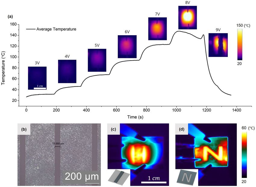
www.nature.com/scientificreports/
Figure 2. Characteristics of Ag NPs generated from PLA of Ag NW in liquid media. (a) Transmission
electron microscopy (TEM) image of Ag NPs. The inset presents the elemental maps and selected area electron
diffraction (SAED) pattern. (b) Size distribution of Ag NPs. The median size and standard deviation were
calculated from Gaussian fitting. (c) Absorbance of the Ag NP solution. The inset shows the yellowish color of
the Ag NP solution.
generally spherical and well-dispersed Ag NPs. Energy dispersive spectrometer (EDS) measurements showed
that the main component of the NPs was silver. It is known that a thin oxide film of several nanometers is usu-
ally formed from the LAL of a silver substrate59. However, no severe surface oxidation was observed during our
measurements (Figs. S1 and S2). Silver was detected as the prominent element owing to the relatively long pen-
etration depth of XRD as reported in previous s tudies60. Selected area electron diffraction (SAED) measurements
also revealed that the crystallinity was consistent with the face-centered cubic structure of silver61. To identify
the size distribution, the TEM images of 100 samples were selected. The diameters of the NPs were calculated
through image processing as shown in Fig. 2b. Although some of the NPs had sizes larger than 20 nm because of
the physical synthesis involved, most of the particles were found to have a size less than 10 nm. From Gaussian
fitting, the mean and the standard deviation of the sizes were observed to be 7.24 nm and 2.67 nm, respectively.
The absorbance and color properties of the NP solution were typical of Ag NPs. From Fig. 2c, it can be observed
that the solution has an absorbance peak around 400 nm, which is identical to the plasmon resonance absorption
peak of Ag N Ps62. A yellowish color, a specific characteristic of Ag NP colloids, was also observed as shown in
the inset. The main difference between the Ag NW layer and a conventional bulk silver plate during the LAL is
that the Ag NPs produced from the former exhibited superior properties compared to the bulk target in terms of
morphology and oxidation. While Ag NPs formed from the Ag NW layer maintained a dispersion of 10 nm or
less, the NPs were often aggregated in the bulk target (Fig. S3a). Figure S3b shows that even the chain shapes of
the connected NPs were because of intensified aggregation under the same processing conditions used for Ag NW
LAL. It was assumed that the different processing results were due to the amount of the ablated material and the
shape of the cavitation bubble. In the case of the bulk target, aggregation can be easily caused because increased
material interaction often occurs within the cavitation bubble formed by the relatively expanded ablated target
material30. Moreover, when a metal wire is ablated in a liquid, the unconventional shape of the cavitation bubble
induces quick detachment of the bubble from the target63,64. Therefore, an improved morphology of Ag NPs was
generated from reduced material interaction and the shape of the cavitation bubble. The Ag NPs formed from
Ag NWs were less affected by surface oxidation. Figure S3e shows the EDS results of the Ag NPs produced from
the Ag plate, indicating that oxygen was detected on the surface of the NPs, which is easily distinguishable from
the surrounding oxygen. When comparing the oxygen content along the line profile (Fig. S3f), it was found that
the Ag NPs from Ag NWs were less affected by oxidation.
To fabricate the Ag NWs decorated with the generated Ag NPs, the EPD process was utilized. The electro-
phoretic motion of Ag NPs according to the applied external voltage can be expressed through Henry’s equation
as follows65:
Scientific Reports | (2021) 11:2262 | https://doi.org/10.1038/s41598-021-81692-9 3
Vol.:(0123456789)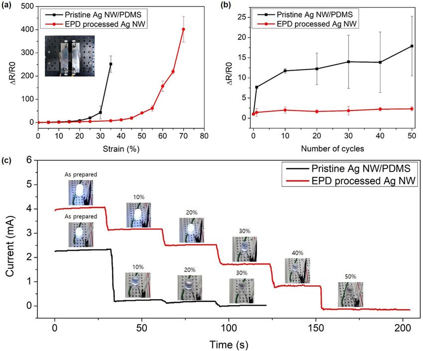
www.nature.com/scientificreports/
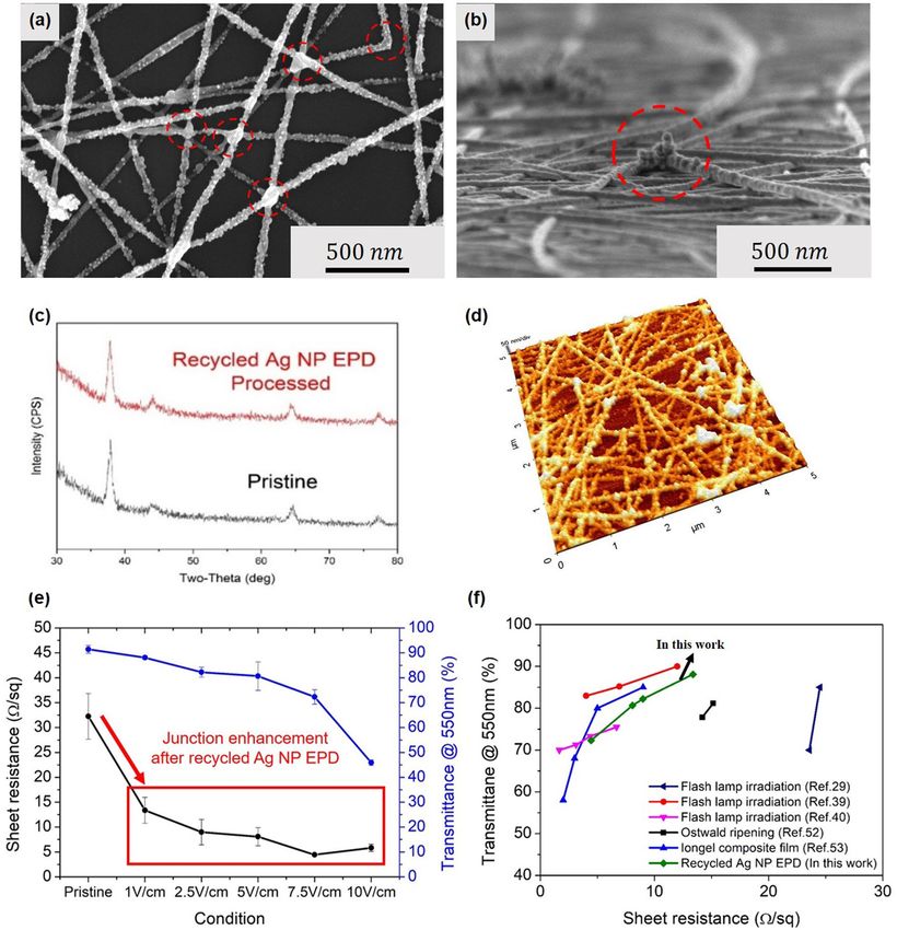
Figure 3. Morphological change of Ag NWs after EPD of recycled Ag NPs. Scanning electron microscopy
(SEM) images of (a) pristine Ag NW and EPD-processed Ag NWs at (b) 1 V/cm, (c) 2.5 V/cm, (d) 5 V/cm, (e)
7.5 V/cm, and (f) 10 V/cm.
ν 2 ε0 εr ξ
µ= = f (κr), (1)
E 3 η
where ε0 is the vacuum permittivity, εr and η are the relative permittivity and viscosity of the liquid, respectively,
and f(κr) is a function depending on the radius (r) and the double layer thickness (κ−1). The movement of NPs
within the electric field is mainly affected by the electric field and the zeta potential of the NPs. As the gener-
ated NPs have a positive zeta potential (Fig. S4), a cathodic EPD process was performed. Figure 3 shows the
surface morphologies of pristine Ag NWs and after performing the EPD process for 10 min. The pristine Ag NW
layer had a diameter of approximately 20 nm and exhibited a typical nanowire percolation network with weak
contact bonding. However, after the EPD of Ag NPs at 1 V/cm, partial deposition of Ag NPs with a diameter
of approximately 40 nm was observed. In particular, owing to the aggregation of Ag NPs on the contact area,
it was found that an enhanced junction was effectively formed even under relatively low voltage conditions. At
2.5 V/cm, the EPD of the NPs was actively conducted to form Ag NWs decorated with Ag NPs. As the voltage
increased, the Ag NPs gradually deposited on the entire surface area of the NWs. Larger Ag NPs were formed
from the aggregated Ag NPs. At 5 V/cm, the morphology was similar to that obtained at 2.5 V/cm. However,
aggregation was observed in some regions decorated with Ag NPs having a diameter above 100 nm. Above an
electric field of 7.5 V/cm, large lumps of Ag NPs (100–200 nm diameter) were formed as many Ag NPs were
deposited simultaneously. Finally, at 10 V/cm, the surface of the Ag NWs was completely covered by the Ag NPs.
The diameter of the Ag NPs exceeded several hundreds of nanometers in this condition. Owing to the enhanced
junction of Ag NWs, the Ag NWs decorated with Ag NPs have better mechanical and electrical properties than
pristine Ag NWs. However, it is essential to select the appropriate voltage conditions because the transparency
decreases as the deposited Ag NPs occupy a larger area.
As the performance of Ag NWs usually depends on the morphology and surface properties, the characteristics
of the EPD-processed Ag NWs were analyzed. Figure 4a shows a scanning electron microscopy (SEM) image
of the Ag NWs after EPD at 2.5 V/cm. It was found that Ag NPs were deposited along the Ag NWs, forming Ag
NWs decorated with Ag NPs. In particular, as shown in the red dashed area, aggregated Ag NPs were formed
in the contact spots of Ag NWs. An enhanced junction due to the deposition of Ag NPs was expected to lower
the contact resistance and increase the mechanical reliability by increasing the contact bonding of Ag NWs. The
tilted SEM image in Fig. 4b shows that strongly bonded Ag NWs are formed from the aggregation of Ag NPs
at the junction region. From the component analysis of the particles attached to the Ag NWs (Fig. S5), it was
confirmed that the recycled Ag NPs were the key materials that strengthened the junction of the Ag NWs. As
shown in Fig. 4c, XRD analysis before and after the EPD process also identified that the generated Ag NPs were
the causes of junction enhancement. As no silver oxide peaks were detected, it was concluded that degradation
due to surface oxidation of Ag NPs was negligible. This result was similar to those of various other studies on
junction welding of Ag NWs processed in liquid media48,66. The surface properties of the Ag NWs decorated with
Ag NPs were revealed by atomic force microscopy (AFM) measurements, as shown in Fig. 4d. After the EPD
process, it was found that the Ag NWs had a rough surface on which particles were agglomerated and bonded
to each other. As the electric field was increased, the surface roughness of the Ag NWs was also increased from
Scientific Reports | (2021) 11:2262 | https://doi.org/10.1038/s41598-021-81692-9 4
Vol:.(1234567890)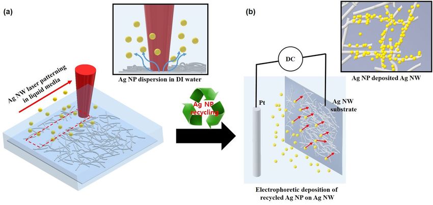
www.nature.com/scientificreports/

                                  Figure 4.  Surface properties and performance of junction-enhanced Ag NWs. (a) Plane image and (b) tilted
                                  SEM image of EPD-processed Ag NWs. (c) XRD spectrum before and after the EPD process. (d) Atomic force
                                  microscopy (AFM) image of Fig. (a). (e) Sheet resistance and transmittance of Ag NWs at 550 nm at different
                                  electric fields. (f) Performance comparison between EPD-processed Ag NWs from recycled Ag NPs and
                                  previously reported junction-welded Ag NWs.

                                  the additional deposition of Ag NPs. As shown in Fig. S6, the pristine Ag NWs are tightly clustered with rela-
                                  tively weak contact bonding. With the application of the electric field (2.5 V/cm), the particles attached along
                                  the NWs, thereby forming Ag NWs decorated with Ag NPs. As the electric field was increased up to 5 V/cm,
                                  the aggregation of Ag NPs intensified, forming a strong bond between the Ag NWs. However, an excessive elec-
                                  tric field induces rapid growth of NPs, which often deteriorates the transparency of the Ag NW substrate. The
                                  changes in the sheet resistance and transmittance were measured at different values of the applied electric field.
                                  Figure 4e shows the sheet resistance and the transmittance of Ag NWs at 550 nm under different electric fields.
                                  When EPD of the Ag NPs was performed, a noticeably decreased contact resistance was observed. At 1 V/cm,
                                  the sheet resistance of the Ag NWs decreased from 32.26 Ω/sq to 13.36 Ω/sq. As the electric field was increased
                                  from 1 to 10 V/cm, the sheet resistance decreased to below 10 Ω/sq. It was believed that this improvement was
                                  due to the increased deposition of Ag NPs on the Ag NWs. However, as the deposition of Ag NPs increased,

Scientific Reports |   (2021) 11:2262 |                https://doi.org/10.1038/s41598-021-81692-9                                                 5

                                                                                                                                             Vol.:(0123456789)
www.nature.com/scientificreports/
Figure 5. Ag NW transparent heater demonstration. (a) Transient temperature evolution of the Ag NW heater
at stepwise voltage increases from 3 to 9 V. (b) Optical image of patterned Ag NWs after PLA. Selective heating
of specific region from patterned Ag NWs; IR image of Ag NWs with the (c) embossed line and (d) engraved
“N” shape. The insets present the ablation regions.
the transparency decreased owing to the increased scattering by Ag NPs (Fig. S7). Pristine Ag NW/glass, after
vacuum filtration, normally has a transmittance of 91% at 550 nm. As the applied electric field increased from
1 to 10 V/cm, the transmittance value reduced from 89.05 to 47.52%. Therefore, in the proposed process, 1 V/
cm with excellent transmittance (89.05% at 550 nm) and low sheet resistance (13.36 Ω/sq) was selected as the
optimal condition to produce Ag NW TCEs. Figure 4f shows the performance comparison of the Ag NP EPD
process with processes used in previous junction welding studies. Although it was not superior, a comparable
level of performance improvement was achieved. The unique advantage of the Ag NP EPD process is that little
additional cost is needed to produce the enhanced junction of Ag NWs. When patterning junction-welded Ag
NWs, welding and patterning are often performed separately39,67. On the other hand, as the recycling process
utilizes the by-products generated from the laser patterning process, patterning and junction strengthening can
be performed in a simple and inexpensive way. Therefore, the proposed process is superior to previous methods
in terms of efficiency and eco-friendliness.
The junction-enhanced Ag NW layer can be utilized in various optoelectronic devices. To demonstrate the
usability of the proposed process, a substrate of Ag NWs decorated with Ag NPs was fabricated as a transparent
heater and its performance was tested. The test was conducted using the method for evaluating the performance
of Ag NWs as transparent heaters in previous studies1,6,7. Figure 5a shows an IR camera image when a DC voltage
is applied to the pristine Ag NW/glass substrate after the EPD at 1 V/cm for 10 min. When the voltage increased
from 3 to 9 V at 3-min intervals, the temperature gradually increased and converged to a constant temperature
under the given conditions. At 8 V, the temperature increased up to 150 ◦ C Although the temperature decreased
after the peak temperature, the performance was not attributed to deterioration from the degradation of the Ag
NWs due to surface oxidation of Ag NWs, which has been reported to occur at higher temperatures1. Instead,
the degradation appeared to be the effect of substrate damage due to thermal stress from the rapid temperature
rise. Under the 9 V condition, the substrate broke into two pieces as the thermal stress was intensified. The high
temperature profile shows that Ag NWs decorated with Ag NPs can be effectively utilized as transparent heaters.
For practical applications of Ag NW TCEs, the patterning process is important depending on the end use. When
patterned Ag NWs are used as transparent heaters, the temperature can be controlled selectively as the current
Scientific Reports | (2021) 11:2262 | https://doi.org/10.1038/s41598-021-81692-9 6
Vol:.(1234567890)www.nature.com/scientificreports/
Figure 6. Electromechanical properties of junction-enhanced Ag NW/PDMS. The resistance changes in the
pristine and EPD-processed Ag NWs depending on (a) the stretching strain and (b) repetitive cycles at 20%
strain. (c) The change in currents in pristine and EPD-processed Ag NWs connected to an LED. Images of the
LED at strains varying from 10% to 50% (3 V).
flow is concentrated in the non-ablated r egion7,68. The patterned Ag NWs decorated with Ag NPs prepared from
the proposed process were evaluated to determine their capability for offering selective temperature control.
During laser patterning of Ag NWs, an arbitrary shape could be produced using a galvanometer scanner with
a line width of ~ 78 μm (Fig. 5b). Figure S8 shows the optical image of the patterned Ag NW substrate with (a)
an embossed line and (b) an engraved “N” shape. Transparent electrodes with desired shapes can be easily pat-
terned through laser ablation. After the laser ablation process, the EPD of recycled Ag NPs was also conducted.
Figure S5c and 5d show the IR images of the patterned substrate. Under the 5 V condition, it was found that
the temperature of the substrate rose to ~ 60 ◦ C. In addition, due to a concentrated current density, significantly
higher temperatures occurred in the non-ablated Ag NWs compared to the surrounding substrate. Accordingly,
through a simple laser patterning process and junction enhancement through EPD, a transparent heater utilizing
Ag NWs, which provided selective temperature control, of the desired shape was easily formed.
The flexibility of Ag NWs, which enables them to operate as TCEs on non-rigid substrates, is one of the main
reasons for their preferred use over ITO. To examine whether the proposed process can be applied to stretchable
substrates, Ag NWs were transferred to polydimethylsiloxane (PDMS), following which EPD of the recycled Ag
NPs was performed. Decreased resistance and transmittance values were observed showing that the experimental
results were similar to those obtained for the glass substrate. After the EPD at 1 V/cm for 10 min, the resistance
decreased from 126.8 Ω to 72.9 Ω, and transmittance at 550 nm decreased from 88 to 85% (Fig. S9). Figure 6a
shows the change in resistance of pristine Ag NWs and EPD-processed Ag NWs depending on the strain. The
strain was adjusted by a micrometer while keeping both ends of the Ag NW/PDMS fixed as shown in the inset.
On comparing the changes in resistance values, the EPD-processed Ag NW layer exhibited better electrical
performance than pristine Ag NWs. In the case of pristine Ag NWs, the resistance change was relatively less
Scientific Reports | (2021) 11:2262 | https://doi.org/10.1038/s41598-021-81692-9 7
Vol.:(0123456789)www.nature.com/scientificreports/
until 20% strain was reached and increased rapidly from 25 to 40% strain, beyond which the resistance was not
measured. On the other hand, the resistance change of EPD-processed Ag NWs was not substantial up to 45%
strain, and the resistance was measured up to 70% strain even after a considerable increase in resistance had
occurred. The resistance change ratio was measured as 14.47 at 40% strain. Similar results were obtained when
the test cycle was performed under the 20% strain condition (Fig. 6b). The EPD-processed Ag NWs exhibited
a relatively small resistance change ratio (2.68) throughout the test cycle, whereas the resistance of pristine Ag
NWs increased continuously due to the relatively weak contact bonding of Ag NWs. With repeated numbers
of cycles, the difference in the resistance change ratio widened. Therefore, the fabricated Ag NWs decorated
with Ag NPs showed better performance as a stretchable TCE than pristine Ag NWs. Finally, patterned Ag
NWs decorated with Ag NPs from the proposed process were examined as a stretchable TCE using the LED
test. An Ag NW layer transferred onto PDMS (226.22 mg/m2) was irradiated with the same fluence as that used
for the glass substrate, i.e., 6.31 J/cm2, and no PDMS substrate damage was observed. The EPD of Ag NPs was
performed on the patterned Ag NW substrate as shown in Fig. S10. The Ag NW substrate was connected in
the middle of the LED circuit, and the LED was turned on by applying a voltage of 3 V. Figure 6c shows a com-
parison of the LED currents for different values of strain on the Ag NW/PDMS substrate. It was observed that
junction-reinforced Ag NWs emitted light under strains up to 40%, but pristine NWs did so up to only a 20%
strain. On comparing the electric current and brightness between junction-reinforced and pristine NWs for the
same strain (20%), the junction-reinforced Ag NWs were found to exhibit improved performance. In another
application, we investigated whether the fabricated substrate could operate as a stretchable heater. As shown in
Fig. S11, the temperature increases up to 40 ◦ C under a voltage of 3 V. Additionally, the substrate could operate
even under a strain of 20%. Accordingly, it was confirmed that the Ag NWs decorated with Ag NPs could be
used as a superior stretchable TCE.
In summary, we propose a minimum-waste laser patterning process by recycling Ag NP debris resulting
from the laser ablation of Ag NWs in liquid media. With the application of liquid media, the Ag residues, which
would normally be discarded, remained well dispersed in an Ag NP solution. The generated Ag NPs showed
superior performance in terms of morphology and oxidation resistance compared to the Ag plating formed via
LAL. Through the EPD of Ag NPs, junction-enhanced Ag NWs decorated with Ag NPs were formed, leading
to improved electrical and mechanical performances of non-ablated Ag NWs. EPD-processed Ag NWs can
be used as transparent heaters with selective temperature control of the laser-patterned Ag NWs. The Ag NW
layer transferred onto PDMS could withstand higher strains and a larger number of test cycles than pristine Ag
NWs, showing that the former can be used as superior stretchable TCEs. As the proposed process improves the
performance of the Ag NWs by utilizing ablated debris that is normally discarded during the laser patterning
process, it is more environmentally friendly and economical than the conventional junction welding process.
Methods
Vacuum filtration of Ag NWs on a substrate. A substrate was prepared for the transfer of Ag NWs.
A 1-in soda-lime glass substrate (SL.Sli1012, SciLab) was used for the characterization and transparent heater
application of Ag NWs decorated with Ag NPs. The PDMS substrate used for testing the stretchable TCE was
prepared by mixing the PDMS solution and curing agent (Sylgard 184, Dow Corning) in a 10:1 ratio. The mix-
ture was heated at 60 ◦ C for 3 h. Ag NWs with a diameter of 21 ± 3 nm and length of 22 ± 5 μm were purchased
(Flexiowire 2020C, Flexio). The Ag NW percolation network layer was transferred by vacuum fi ltration7,69.
Nylon (7402-004, Whatman) and polytetrafluoroethylene (PTFE) filters (190455-1LSC, STERLITECH) were
placed on a microassay holder. While maintaining vacuum, 10 ml of isopropyl alcohol (IPA) (HPLC grade,
Sigma-Aldrich) with the Ag NW solution was poured into the PTFE filter. The areal densities of Ag NWs were
113.11, 169.67, and 226.22 mg/m2 for glass, PDMS, and patterned PDMS substrates, respectively. The substrate
(glass/PDMS) was placed in the filter for 1 min so that the Ag NWs could be in contact with the substrate.
Thereafter, the vacuum was released, the substrate was gently removed from the filter, and an Ag NW percolation
network on the substrate was formed.
Laser patterning of Ag NWs. To fabricate patterned Ag NWs, an ytterbium fiber laser with a wavelength
of 1060 nm (YLD-D30, Han’s Laser Technology Co., Ltd; pulse width = 200 ns, repetition rate = 20 kHz, output
power = 24 W) was used. It was focused using an f-theta lens with a focal length of 150 mm and a two-dimen-
sional galvanometer scanner. In the line patterning process, the scan speed was 100 mm/s, and in the area pat-
terning process, such as text patterning, the hatch of the line pattern was set to 0.05 mm so that the entire area
was removed. The laser ablation of Ag NWs in the liquid media was prepared by carefully dipping Ag NWs in
DI water (LC–MS Grade, Merck) contained in a Petri dish (DU.2175541, Duran). In the immersed condition,
the substrate was irradiated with a fluence of 6.31 J/cm2. After the patterning process, the patterned Ag NW
substrate was gently removed using tweezers, followed by blowing with nitrogen gas. A yellowish Ag NP solution
was found in the Petri dish after the irradiation. The generated Ag NPs were transferred to a beaker and used
for the EPD.
EPD of Ag NPs onto the unpatterned Ag NWs substrate. The Ag NPs generated via recycling were
subjected to EPD. A common power supply (U8001A, KEYSIGHT) was used to apply a constant electric field,
which was controlled by varying the voltage and distance between the substrates. The distance between the sub-
strates was fixed at 1 cm, and the electric field was changed by increasing the voltage from 1 to 10 V. For cathodic
EPD, the cathode was connected to the patterned Ag NW substrate, and the platinum electrode (CE-POST-Pt-
01-05-PTFE-06-80, WIZMAC) was connected to the anode. After the two electrodes were immersed in the Ag
Scientific Reports | (2021) 11:2262 | https://doi.org/10.1038/s41598-021-81692-9 8
Vol:.(1234567890)www.nature.com/scientificreports/
NP solution, EPD was conducted for 10 min through voltage application. After EPD, the Ag NW substrate was
rinsed with deionized water (DI water), followed by gentle blowing with nitrogen gas.
Characterization. TEM (Talos F200X) was used to examine the Ag NP debris after PLA of Ag NWs in
liquid media. The particle size was calculated from 100 TEM images using the Image J software. The mean size
and the standard deviation were obtained by fitting the size frequency diagram to a Gaussian function (Origin
8.1). The absorbance of the generated Ag NPs and transmittance of the Ag NWs were measured using an ultra-
violet–visible spectrometer (Evolution 220, Thermo Fisher Scientific), and the zeta potential was measured using
Zetasizer Nano ZS (Malvern Panalytical). The surface morphologies of the Ag NWs were identified from SEM
(NOVA 230, FEI) and AFM (XE-100, Park Systems). The sheet resistances were measured using a 4-point probe
(FPP-400, DASOLENG). The components of the Ag NPs and Ag NWs were analyzed using an EDS and XRD
(X’Pert-PRO MRD, PANalytical). For real-time temperature measurements of the stretchable Ag NW TCE, an
infrared IR camera (A35, FLIR) was used.
Received: 16 October 2020; Accepted: 11 January 2021
References
1. Jang, J. et al. Rapid production of large-area, transparent and stretchable electrodes using metal nanofibers as wirelessly operated
wearable heaters. NPG Asia Mater. 9, e432–e432 (2017).
2. Lee, C. et al. Flash-induced nanowelding of silver nanowire networks for transparent stretchable electrochromic devices. Sci. Rep.
8, 1–10 (2018).
3. Jin, Y., Deng, D., Cheng, Y., Kong, L. & Xiao, F. Annealing-free and strongly adhesive silver nanowire networks with long-term
reliability by introduction of a nonconductive and biocompatible polymer binder. Nanoscale 6, 4812–4818 (2014).
4. Cho, S. et al. Large-area cross-aligned silver nanowire electrodes for flexible, transparent, and force-sensitive mechanochromic
touch screens. ACS Nano 11, 4346–4357 (2017).
5. Shin, K. et al. Patterned transparent electrode with a continuous distribution of silver nanowires produced by an etching-free
patterning method. Sci. Rep. 7, 1–10 (2017).
6. Seok, H.-J., Kim, J.-K. & Kim, H.-K. Effective passivation of Ag nanowire network by transparent tetrahedral amorphous carbon
film for flexible and transparent thin film heaters. Sci. Rep. 8, 13521 (2018).
7. Hong, S. et al. Highly stretchable and transparent metal nanowire heater for wearable electronics applications. Adv. Mater. 27,
4744–4751 (2015).
8. Amjadi, M., Pichitpajongkit, A., Lee, S., Ryu, S. & Park, I. Highly stretchable and sensitive strain sensor based on silver nanowire-
elastomer nanocomposite. ACS Nano 8, 5154–5163 (2014).
9. Hsu, P.-C. et al. Personal thermal management by metallic nanowire-coated textile. Nano Lett. 15, 365–371 (2015).
10. Won, P. et al. Stretchable and transparent Kirigami conductor of nanowire percolation network for electronic skin applications.
Nano Lett. 19, 6087–6096 (2019).
11. Lee, D. J., Oh, Y., Hong, J.-M., Park, Y. W. & Ju, B.-K. Light sintering of ultra-smooth and robust silver nanowire networks embed-
ded in poly(vinyl-butyral) for flexible OLED. Sci. Rep. 8, 14170 (2018).
12. Kang, H. et al. Flexible and mechanically robust organic light-emitting diodes based on photopatternable silver nanowire electrodes.
J. Phys. Chem. C 120, 22012–22018 (2016).
13. Lee, E. et al. All-solution-processed silver nanowire window electrode-based flexible perovskite solar cells enabled with amorphous
metal oxide protection. Adv. Energy Mater. 8, 1702182 (2018).
14. Benatto, G. A. D. R. et al. Roll-to-roll printed silver nanowires for increased stability of flexible ITO-free organic solar cell modules.
Nanoscale 8, 318–326 (2015).
15. Liu, S., Ho, S. & So, F. Novel patterning method for silver nanowire electrodes for thermal-evaporated organic light emitting diodes.
ACS Appl. Mater. Interfaces 8, 9268–9274 (2016).
16. Ko, Y. et al. A simple silver nanowire patterning method based on poly(ethylene glycol) photolithography and its application for
soft electronics. Sci. Rep. 7, 1–9 (2017).
17. Finn, D. J., Lotya, M. & Coleman, J. N. Inkjet printing of silver nanowire networks. ACS Appl. Mater. Interfaces 7, 9254–9261 (2015).
18. Chen, S. et al. A water-based silver nanowire ink for large-scale flexible transparent conductive films and touch screens. J. Mater.
Chem. C 5, 2404–2414 (2017).
19. Hong, S. et al. Selective laser direct patterning of silver nanowire percolation network transparent conductor for capacitive touch
panel. J. Nanosci. Nanotechnol. 15, 2317–2323 (2015).
20. Oh, H. & Lee, M. Laser-direct fabrication of invisible Ag nanowire electrode pattern on flexible plastic substrate. Thin Solid Films
636, 375–383 (2017).
21. Madaria, A. R., Kumar, A., Ishikawa, F. N. & Zhou, C. Uniform, highly conductive, and patterned transparent films of a percolating
silver nanowire network on rigid and flexible substrates using a dry transfer technique. Nano Res. 3, 564–573 (2010).
22. Li, J. et al. A flexible plasma-treated silver-nanowire electrode for organic light-emitting devices. Sci. Rep. 7, 16468 (2017).
23. Oh, H., Lee, J., Kim, J.-H., Park, J.-W. & Lee, M. Fabrication of invisible Ag nanowire electrode patterns based on laser-induced
Rayleigh instability. J. Phys. Chem. C 120, 20471–20477 (2016).
24. Oh, H. & Lee, M. Laser-induced electrical property patterning of Ag nanowire transparent electrode. Mater. Lett. 176, 110–113
(2016).
25. Oh, H. & Lee, M. Comparative analysis of serial and parallel laser patterning of Ag nanowire thin films. Appl. Surf. Sci. 399, 617–623
(2017).
26. Henley, S. J., Cann, M., Jurewicz, I., Dalton, A. & Milne, D. Laser patterning of transparent conductive metal nanowire coatings:
simulation and experiment. Nanoscale 6, 946–952 (2013).
27. Nishi, N. et al. Effects of pulse duration on removal characteristics of silver nanowire transparent conductive film by nanosecond
pulsed laser. J. Mater. Process. Technol. 240, 255–261 (2017).
28. Cann, M. et al. High performance transparent multi-touch sensors based on silver nanowires. Mater. Today Commun. 7, 42–50
(2016).
29. Yoo, B., Kim, Y., Han, C. J., Oh, M. S. & Kim, J.-W. Recyclable patterning of silver nanowire percolated network for fabrication of
flexible transparent electrode. Appl. Surf. Sci. 429, 151–157 (2018).
Scientific Reports | (2021) 11:2262 | https://doi.org/10.1038/s41598-021-81692-9 9
Vol.:(0123456789)www.nature.com/scientificreports/
30. Zhang, D., Gökce, B. & Barcikowski, S. Laser synthesis and processing of colloids: Fundamentals and applications. Chem. Rev. 117,
3990–4103 (2017).
31. Ratti, M. et al. Production of metal nanoparticles by pulsed laser-ablation in liquids: A tool for studying the antibacterial properties
of nanoparticles. J. Vis. Exp. 124, e55416. https://doi.org/10.3791/55416 (2017).
32. Yan, Z. & Chrisey, D. B. Pulsed laser ablation in liquid for micro-/nanostructure generation. J. Photochem. Photobiol. C Photochem.
Rev. 13, 204–223 (2012).
33. Guo, W. & Liu, B. Liquid-phase pulsed laser ablation and electrophoretic deposition for chalcopyrite thin-film solar cell applica-
tion. ACS Appl. Mater. Interfaces 4, 7036–7042 (2012).
34. He, H., Cai, W., Lin, Y. & Chen, B. Au nanochain-built 3D netlike porous films based on laser ablation in water and electrophoretic
deposition. Chem. Commun. 46, 7223–7225 (2010).
35. He, H., Lin, Y., Liu, G. & Cai, W. Au nanoparticle-built mesoporous films based on co-electrophoresis deposition and selective
etching. Electrochem. Commun. 46, 71–74 (2014).
36. Semaltianos, N. G., Hendry, E., Chang, H. & Wears, M. L. Electrophoretic deposition on graphene of Au nanoparticles generated
by laser ablation of a bulk Au target in water. Laser Phys. Lett. 12, 046201 (2015).
37. Yang, S., Cai, W., Liu, G. & Zeng, H. From nanoparticles to nanoplates: preferential oriented connection of Ag colloids during
electrophoretic deposition. J. Phys. Chem. C 113, 7692–7696 (2009).
38. Fernández-Arias, M. et al. Synthesis and deposition of Ag nanoparticles by combining laser ablation and electrophoretic deposition
techniques. Coatings 9, 571 (2019).
39. Park, J. H. et al. Flash-induced self-limited plasmonic welding of silver nanowire network for transparent flexible energy harvester.
Adv. Mater. 29, 1603473 (2017).
40. Jiu, J. et al. Strongly adhesive and flexible transparent silver nanowire conductive films fabricated with a high-intensity pulsed light
technique. J. Mater. Chem. 22, 23561–23567 (2012).
41. Jiu, J. et al. High-intensity pulse light sintering of silver nanowire transparent films on polymer substrates: The effect of the thermal
properties of substrates on the performance of silver films. Nanoscale 5, 11820–11828 (2013).
42. Jang, Y.-R. et al. Selective Wavelength Plasmonic Flash Light Welding of Silver Nanowires for Transparent Electrodes with High
Conductivity. ACS Appl. Mater. Interfaces 10, 24099–24107 (2018).
43. Hu, L., Kim, H. S., Lee, J.-Y., Peumans, P. & Cui, Y. Scalable coating and properties of transparent, flexible, silver nanowire elec-
trodes. ACS Nano 4, 2955–2963 (2010).
44. Menamparambath, M. M. et al. Silver nanowires decorated with silver nanoparticles for low-haze flexible transparent conductive
films. Sci. Rep. 5, 1–9 (2015).
45. Lee, J. et al. Silver nanowires: Room-temperature nanosoldering of a very long metal nanowire network by conducting-polymer-
assisted joining for a flexible touch-panel application. Adv. Funct. Mater. 23, 4165–4165 (2013).
46. Ahn, Y., Jeong, Y. & Lee, Y. Improved thermal oxidation stability of solution-processable silver nanowire transparent electrode by
reduced graphene oxide. ACS Appl. Mater. Interfaces 4, 6410–6414 (2012).
47. Liang, J. et al. Silver nanowire percolation network soldered with graphene oxide at room temperature and its application for fully
stretchable polymer light-emitting diodes. ACS Nano 8, 1590–1600 (2014).
48. Eom, H. et al. Ag@Ni core-shell nanowire network for robust transparent electrodes against oxidation and sulfurization. Small
10, 4171–4181 (2014).
49. Kang, H. et al. Epitaxial-growth-induced junction welding of silver nanowire network electrodes. ACS Nano 12, 4894–4902 (2018).
50. Wang, S., Tian, Y., Hang, C. & Wang, C. Cohesively enhanced electrical conductivity and thermal stability of silver nanowire
networks by nickel ion bridge joining. Sci. Rep. 8, 1–9 (2018).
51. Lee, H.-J. et al. Spontaneous and selective nanowelding of silver nanowires by electrochemical Ostwald ripening and high electro-
static potential at the junctions for high-performance stretchable transparent electrodes. ACS Appl. Mater. Interfaces 10, 14124–
14131 (2018).
52. Xiong, W. et al. Highly conductive, air-stable silver nanowire@iongel composite films toward flexible transparent electrodes. Adv.
Mater. 28, 7167–7172 (2016).
53. Liu, B.-T. & Huang, S.-X. Transparent conductive silver nanowire electrodes with high resistance to oxidation and thermal shock.
RSC Adv. 4, 59226–59232 (2014).
54. Kruusing, A. Underwater and water-assisted laser processing: Part 1—General features, steam cleaning and shock processing. Opt.
Lasers Eng. 41, 307–327 (2004).
55. Kruusing, A. Underwater and water-assisted laser processing: Part 2—Etching, cutting and rarely used methods. Opt. Lasers Eng.
41, 329–352 (2004).
56. Ouyang, P., Li, P., Leksina, E. G., Michurin, S. V. & He, L. Effect of liquid properties on laser ablation of aluminum and titanium
alloys. Appl. Surf. Sci. 360, 880–888 (2016).
57. Xu, X. et al. Fabrication of gold nanoparticles by laser ablation in liquid and their application for simultaneous electrochemical
detection of C d2+, Pb2+, Cu2+, Hg2+. ACS Appl. Mater. Interfaces 6, 65–71 (2014).
58. Shafeev, G. A. et al. Generation of Au nanorods by laser ablation in liquid and their further elongation in external magnetic field.
Appl. Surf. Sci. 466, 477–482 (2019).
59. Giorgetti, E. et al. Ag nanoparticles obtained by pulsed laser ablation in water: surface properties and SERS activity. J. Raman
Spectrosc. 46, 462–469 (2015).
60. Kohsakowski, S. et al. High productive and continuous nanoparticle fabrication by laser ablation of a wire-target in a liquid jet.
Appl. Surf. Sci. 403, 487–499 (2017).
61. Cai, Y. et al. Large-scale and facile synthesis of silver nanoparticles via a microwave method for a conductive pen. RSC Adv. 7,
34041–34048 (2017).
62. Nikov, Ru. G. et al. Characterization of Ag nanostructures fabricated by laser-induced dewetting of thin films. Appl. Surf. Sci. 374,
36–41 (2016).
63. Giacomo, A. D. et al. Cavitation dynamics of laser ablation of bulk and wire-shaped metals in water during nanoparticles produc-
tion. Phys. Chem. Chem. Phys. 15, 3083–3092 (2013).
64. Messina, G. C. et al. Pulsed laser ablation of a continuously-fed wire in liquid flow for high-yield production of silver nanoparticles.
Phys. Chem. Chem. Phys. 15, 3093–3098 (2013).
65. Zhang, H. et al. Direct assembly of large area nanoparticle arrays. ACS Nano 12, 7529–7537 (2018).
66. Liu, J. et al. Electrophoresis deposition of flexible and transparent silver nanowire/graphene composite film and its electrochemical
properties. J. Alloys Compd. 745, 370–377 (2018).
67. Park, K. et al. High-resolution and large-area patterning of highly conductive silver nanowire electrodes by reverse offset printing
and intense pulsed light irradiation. ACS Appl. Mater. Interfaces 11, 14882–14891 (2019).
68. Han, S. et al. Nanorecycling: Monolithic integration of copper and copper oxide nanowire network electrode through selective
reversible photothermochemical reduction. Adv. Mater. 27, 6397–6403 (2015).
69. Jung, J. et al. Highly stretchable and transparent electromagnetic interference shielding film based on silver nanowire percolation
network for wearable electronics applications. ACS Appl. Mater. Interfaces 9, 44609–44616 (2017).
Scientific Reports | (2021) 11:2262 | https://doi.org/10.1038/s41598-021-81692-9 10
Vol:.(1234567890)www.nature.com/scientificreports/
Acknowledgements
This work was supported by the Basic Science Research Program (2017R1D1A1B03031307, 2018R1A2B6007500
and 2020R1I1A1A01065476) funded by the National Research Foundation (NRF) under the Ministry of Science.
Author contributions
J.S.H. proposed the concept of this work, carried out the experiment, and wrote the manuscript. J.-E.P and
G.W.K helped the measurement of surface morphologies and H.N, J.S.J and S.K helped the measurement of the
electrical and optical performance of Ag NW TCE. S.Y helped the measurement of the IR camera image. H.L
and M.Y. administrated the whole process of the research.
Competing interests
The authors declare no competing interests.
Additional information
Supplementary Information The online version contains supplementary material available at https://doi.
org/10.1038/s41598-021-81692-9.
Correspondence and requests for materials should be addressed to H.L. or M.Y.
Reprints and permissions information is available at www.nature.com/reprints.
Publisher’s note Springer Nature remains neutral with regard to jurisdictional claims in published maps and
institutional affiliations.
Open Access This article is licensed under a Creative Commons Attribution 4.0 International
License, which permits use, sharing, adaptation, distribution and reproduction in any medium or
format, as long as you give appropriate credit to the original author(s) and the source, provide a link to the
Creative Commons licence, and indicate if changes were made. The images or other third party material in this
article are included in the article’s Creative Commons licence, unless indicated otherwise in a credit line to the
material. If material is not included in the article’s Creative Commons licence and your intended use is not
permitted by statutory regulation or exceeds the permitted use, you will need to obtain permission directly from
the copyright holder. To view a copy of this licence, visit http://creativecommons.org/licenses/by/4.0/.
© The Author(s) 2021
Scientific Reports | (2021) 11:2262 | https://doi.org/10.1038/s41598-021-81692-9 11
Vol.:(0123456789)You can also read