Simulate with Physical and Scalable Discrete Models - What could we get ? - ON ...
←
→
Page content transcription
If your browser does not render page correctly, please read the page content below

Simulate with Physical
 and Scalable Discrete Models…

 What could we get ?

1
Content

 o Brief review of ON Modeling Technique
 o Simulate Devices to Extract Parameters
 o Application Simulations

 2
Modeling Technique (Brief)

 Physical and Scalable

3
Physical SPICE models - benefits

 Closer matching of simulation results to device performances or behaviours
 • Device physics equations inside the model
 • Technology based with measurement calibration, not just curve fitting
 • Fully scalable (all the geometry/dimensions included)
 • Thermal simulation (using electro-thermal equivalence)
 • Reverse recovery behaviour and all non-linear effects
 • Effects of parasitics at circuit, package and die level

 4
Supporting Multiple Simulators
• SPICE Agnostic model is important
 • Only use least common denominator features, PSPICE syntax
• The following simulators are supported:
 • PSpice
 • LTspice
 • SIMetrix
 • Spectre
 • SABER
 • Simplorer
 • Microcap
 • ADS
 • HSPICE
 • Eldo

 5
Example: SiC MOSFET Process Parameter Based Model

 Device Cross Section Sample Physical Model Parameters

 Parameter Description
 Lpoly Gate length
 tox Gate oxide thickness
 dpw JFET opening (distance between pwells)
 Xjpw Pwell junction deping
 CP Cell pitch
 Njfet JFET region doping
 Nepi Epi doping
 Lepi Epi thickness

 Published at APEC 2017
 6
Example : Chip Floor Plan Considerations
Parameter Description
Wchip Chip Width Wchip
Hchip Chip Height

 Hchip
Ngrunner Number of Gate Runners
Wgatepad Gate Pad Width
Hgatepad Gate Pad Height
GatePadLoc Gate Pad Location

 All parasitic capacitance, linear
 and nonlinear, from the non-active
 blue areas are accounted for: “W” MOSFET
 Edge Termination area,
 Gate Pad, “M” MOSFET
 Gate Runners

 Published at APEC 2017
 7
Example : Physical Derivation of CGD (CRSS)

 Cox Doping
 Cdep Wdep1
 Wdep2
 Wdep3

 Wdep4

 Wdep3 represents the drop of the bottom plate of the depletion region once
 the JFET region pinches off.

 Wdep4 is post-pinchoff depletion controlled by Nepi and limited by the Published APEC 2017
 thickness of the Epi.

 8
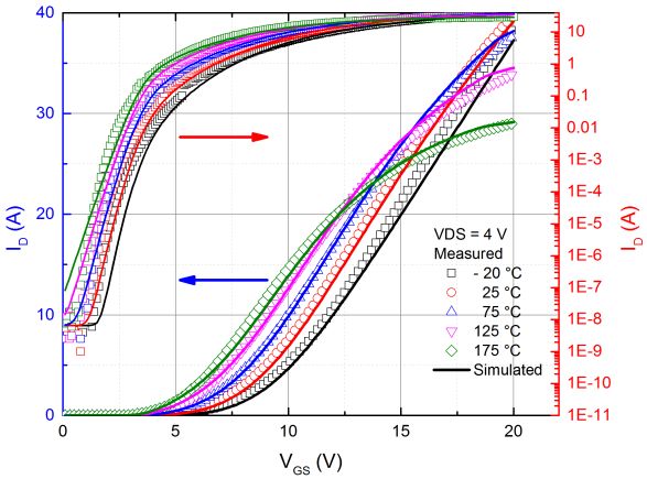
Typical Model Verification – SiC MOSFET Temperature Behaviour

 IDVD IDVG Body Diode

 RDSON VTH Body Diode

 Published at APEC 2017
 9
Typical Model Verification – SiC MOSFET Capacitance Behaviour

 Complex circuit-device interactions are strongly dependant on the device capacitance. The physical models
 provide a fully process dependent derivation of capacitance, enabling realistic dynamic simulation.

 10
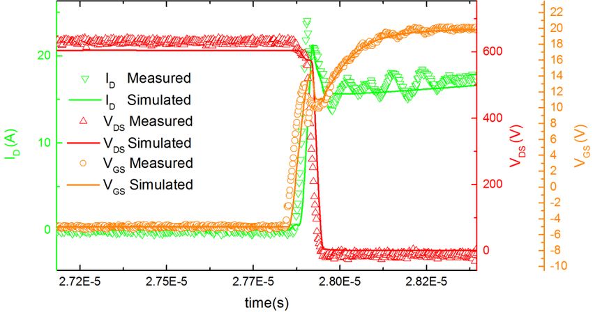
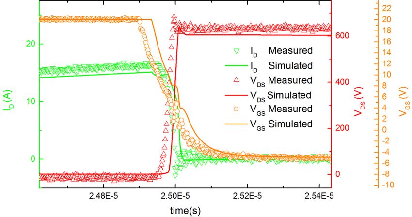
Typical Model Verification – SiC MOSFET Double Pulse
 15 A / 25 °C

Physical models can precisely OFF ON
predict dv/dt, dI/dt and gate
voltage transient enabling
designer to :
• predict switching loss
 15 A / 175 °C
• study EMI
• consider design transient
 immunity
• study gate-circuit interactions

 OFF ON

 Published at APEC 2017
 11
Example : SuperFET™ Accurate Switching Modeling
 OFF Reverse
 Recovery

 ON

 Data: black lines
 Model: color lines
 12
Bibliography

 [1] “Physically Based, Scalable SPICE Modeling Methodologies for Modern
 Power Electronic Devices”
 https://www.onsemi.com/pub/Collateral/TND6260-D.PDF
 [2] “SPICE Modeling Tutorial”,
 https://www.onsemi.com/pub/Collateral/TND6248-D.PPTX
 [3] “How to use Physical and Scalable Models with SIMetrix, OrCAD and
 LTSpice”
 https://www.onsemi.com/pub/Collateral/AND9783-D.PDF
 [4] “Using Physical and Scalable Simulation Models to Evaluate Parameters
 and Application Results”
 https://www.onsemi.com/pub/Collateral/TND6330-D.PDF

 13
Simulate devices : Let’s practice !

 ? Is it easy and useful ?
 ? What can kind of results could be obtained ?

14
On-Region simulation

 Drain Current vs Drain-to-Source Voltage

15
MOSFET On-Region – Books’ Curve

 In books, we found the following on-
 region curves.

 Ohmic Active
 We have two regions:
 - Ohmic and Active
 Cutoff

 This is well known but in practice, this
 curve can be slightly different.
 < < < <

 16
MOSFET On-Region – Data Sheet Curve For the NTHL040N65S3F, SuperFET3 Fast recovery 40 m The data sheet give the following curve with Log-Log scales. This curve is done with a 250-µs pulse test to avoid the MOSFET to heat… 17
MOSFET On-Region - Schematic

 The schematic is very simple :
 VDrain

 • The MOSFET
 I-V
 XY Probe

 • A Drain-to-Source voltage source
 • A Gate-to-Source voltage source NTHL040N65S3F_3p

 That’s all you need…
 Q
 VDD
 VGG

 We add a “X-Y Probe” pseudo-
 component to pre-set the output
 graph.

 18
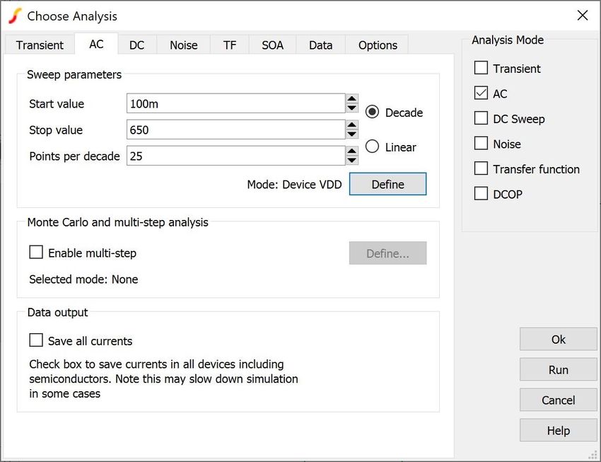
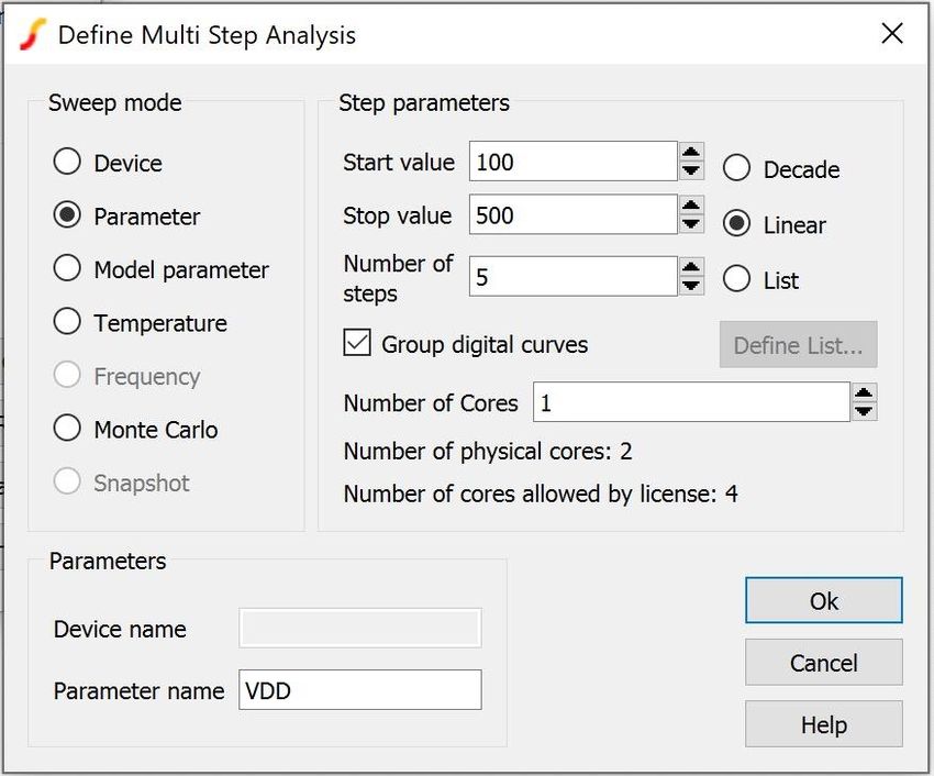
MOSFET On-Region – Setup 1

 We define the
 simulation as
 “DC Sweep” on
 “VDD” source

 We define the
 variation
 amplitude.

 We enable the
 “Multi-Step”
 analysis to vary
 the “VGG” source
 by discrete steps
 19
MOSFET On-Region – Setup 2

 We define the
 values “VGG”
 voltage source
 can take as a list.

 We have the same
 list as the
 specification.

 20
MOSFET On-Region - Results

 Linear scales Logarithmic scales

 21
MOSFET On-Region - Schematic

 We re-use the same simulation
 schematic for a Medium Voltage
 VDrain
 I-V

 MOSFET : NTMFS5C604N.
 XY Probe

 NTHL040N65S3F_3p

 Q
 VDD
 VGG

 22
MOSFET On-Region - Results

 The results are far above maximum
 current capability given in the
 specification for the MOSFET

 The active region is not really
 horizontal

 23
MOSFET On-Region with 5-pin model - Schematic
We will use a 5-pin device to see the VDrain
I-V
temperature behavior during this test. XY Probe
Y
Temp
The model uses the electro-thermal X
equivalence where Voltage represents the
Temperature and the Current represents the
Power dissipated. The case temperature is set NTMFS5C604N_5P Tj
to the system temperature using a voltage Tj VDD
source. The voltage-source value is set with Q Tcase
the SIMetrix variable “Temp” storing the Solv
system temperature. {Temp} 1Meg
VGG TCase
We need to add a 1-M resistor on the
“Junction Temperature” pin to help the solver
to converge.
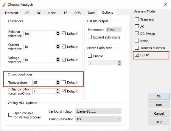
24MOSFET On-Region with 5-pin model – Temperature Setup In the option tab inside simulation setup windows, The system temperature can be set to 25 °C 25
MOSFET On-Region with 5-pin model - Results
 600

 500
 For VGS = 4 V, we see a thermal
 Tj(Q) / °C

 runaway in the saturation region. The
 400

 300
 VGS=9V junction temperature rises above
 200

 175°C
 VGS=5V
 175°C before the drain current
 100
 VGS=4V
 reaches the 280 A specification limit.
 25
 0 0.5 1 1.5
 2 2.5
 3 3.5
 4 4.5 For VGS = 5 V, the device stays in the
 VDS/V 500mV/div
 ohmic region but the junction
 300 temperature rises to 175°C before it
 250
 280A gets to 280-A drain current limit.
 200
 For VGS = 9 V, the device stays in the
 ID / A

 150 ohmic region but the drain current
 100 rises to 280 A limit before it gets to
 50 Thermal runaway 175°C junction temperature.
 0
 0 0.5 1 1.5
 2 2.5
 3 3.5
 4 4.5
 VDS/V 500mV/div

 26
MOSFET On-Region within the limits - Schematic
 We set IDD current source to 280 A.
 We use a switch with very low on- VDrain
 I-V

 resistance driven by the junction XY Probe

 Y

 temperature to short the current Temp

 source when the temperature gets X

 above 175°C.
 We implement a very large hysteresis Tj

 to avoid a new turn on when the NTMFS5C604N_5P Tj
 Q

 device cools down. Tcase
 SC
 Solv
 {Temp} 1Meg
 VGG TCase

 IDD

 1m Pulse(0 280 0 1 1 0 2)

 27
MOSFET On-Region within the limits - Results 6V 7V S= S= 160 5V 5V VG VG S= VGS=4V 4. This is the real useful curves for 25°C S= VG 8V 140 VG S= Tj(Q) / °C 10V VG package temperature. 120 S= VG 100 80 60 40 25 0.5 1.5 2.5 0 1 2 3 VDS/V Thermal runaway 500mV/div Using simulation, we can have the real VGS=10V VGS=8V VGS=7V operating curves in real conditions. 250 VGS=6V 200 ID / A VGS=5V 150 VGS=4.5V 100 50 VGS=4V 0 0.5 1.5 2.5 0 1 2 3 VDS/V 500mV/div 28
MOSFET On-Region within the limits - Schematic

 With the NTHL040N65S3F, we can VDrain

 applied the same setup. I-V
 XY Probe
 SC

 We use a switch with very high off-
 resistance driven by the junction
 temperature to open the voltage
 source when the temperature gets NTHL040N65S3F_5p Tj
 Tj

 above 150°C.
 Q
 Tcase

 We implement a very large hysteresis VGG
 {Temp}
 TCase
 Solv
 1Meg

 to avoid a new turn on when the VDD
 device cools down.
 1m Pulse(0 20 0 1 1 0 2)

 29
Comparing ID-VDS graph for the NTHL040N65S3F 3 pins model Data Sheet 5 pins model 3 different results… With 3 pins model, the die is “some how” maintained at constant temperature (or like if measurement was done with an infinite small pulse) Data sheet use 250µs pulse for measurement. With 5 pins model, measurement are done in DC (infinite long pulse) 30
RDS(on) simulation

 vs Drain Current or Temperature or Time

31
RDS(on) vs Drain Current - Schematic

 We connected a current source
 between the drain and source pin. VDrain
 V(P)/I(Sns) RDSon
 RDSon

 To calculate the RDS(on), we use an I(sns)
 Ron-I
 XY Probe

 arbitrary source to make the division
 OUT

 between drain-to-source voltage by the
 p

 drain current. We obtain a voltage NTHL040N65S3F_3p

 directly proportional to the “on”
 resistance.
 Q
 IDD
 VGG

 We add a “X-Y Probe” pseudo-
 component to pre-set the output
 graph.

 32
RDS(on) vs Drain Current - Results

 We can see a slight difference
 between simulation with the
 NTHL040N65S3F model and the data
 sheet curve.
 In fact, for a 100-A ID and a 10-V VGS,
 the difference is almost 1.25 mΩ.
 This corresponds to a 3% relative
 difference.

 This is acceptable.

 33
RDS(on) vs Temperature - Schematic
We use almost the same schematic,
VDrain
V(P)/I(Sns)/RDSon25C RDSon
Except :
RDSon
I(sns)
OUT
RDSon-Temperature
XY Probe
- The current is fixed at 32.5 A,
p
33.5196m
- A voltage source to represent the
ambient temperature,
Q
NTHL040N65S3F_3p
32.5
IDD
- We add a “Bus annotation marker”
10
VGG
VTemp
to have the RDS(on) at 25°C.
{Temp}
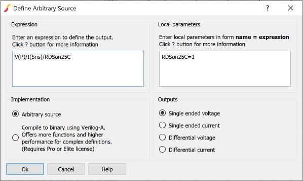
34RDS(on) vs Temperature – Setup 1 Here is the arbitrary function definition with the parameter used to normalize the curve 35
RDS(on) vs Temperature – Setup 2

 Here, we define the setup
 to obtain the 25-°C RDS(on)
 value by setting the
 operating point values.
 Them, we define the
 analyze temperature range

 36
RDS(on) vs Temperature – Results

 On the schematic, we can read the
 25−°C value for the RDS(on).

 This value will be used as parameter
 value for arbitrary function for the next
 simulation.

 37
RDS(on) vs Temperature – Results Normalized

 Around 140°C, the RDS(on) value is
 twice the 25-°C value.

 38
RDS(on) vs Time - Schematic

 The 5-pin models are very useful when
 VDrain

 you want to know the junction
 V(P)/I(Sns)
 RDSon

 temperature behavior depending on
 RDS
 I(sns)
 OUT RDS
 the mission profile.
 p

 Here, we analyze a low frequency Tj

 switching schematic and the impact ID
 NTHL040N65S3F_5p
 Tj
 Tj

 on junction temperature. Q Tcase

 Solv
 10 {Temp} 1Meg
 VGG TCase

 IDD

 Pulse(1 40 50m 1m 1m 24m 50m)

 39
RDS(on) vs Time - Results We can notice the sudden change in the channel resistance when the drain current changes rapidly from 1 A to 40 A and backward. This phenomenon was predicted by the curve Channel resistance vs Drain current. We also see the effect of the self-heating or cooling of the device itself during the plateau phase of the current (1 A and/or 40 A). The system is stable after a 200-ms transient. The maximum junction temperature is 36 °C and the minimum 30 °C. The junction temperature oscillates between those two values. 40
Transfer characteristic

 Drain Current vs Gate-to-Source Voltage

41
Transfer Characteristic - Schematic

 The transfer characteristic shows how VDrain

 the drain current changes with the ID-VGS

 gate-to-source voltage. XY Probe

 The simulation was done with a 20-V
 drain-to-source voltage and for various NTHL040N65S3F_3p

 temperature values.
 We will use a X-Y probe to plot the Q
 20
 VDD
 transfer characteristic and the VGG

 temperature will be set via the “Multi-
 Step” simulation list.

 42
Transfer Characteristic - Results

 We can see the difference for the gate
 threshold in function of temperature.

 43
Output Capacitor

 Small Signal, Effective, Energy related or Charge related

44
Output Capacitor

 For switching application, the output There are 3 to 4 types of output-
 capacitor called Coss defined as capacitance values found in the
 = C + @ = 0 V specification.
 is an important parameter as it has an The capacitance types are called:
 impact on the transistor switching
 losses. In fact, every time the MOSFET • Small-signal value,
 turn on, the energy stored in output • Effective value,
 capacitance is discharged and lost in • Energy-related value,
 the transistor. The lower Coss is the
 better. Coss is a non-linear capacitance • Charge-related value.
 and highly depends on the drain-to-
 source voltage.

 45
Output Capacitor Small-signal - Schematic

 For the signal signal value, we will use the
 following equation :
 1 VDrain
 = ×
 2 ×
 – –
 ID
 – – – –
 Q
 We will use 20-mV peak-to-peak NTHL040N65S3F_3p
 sinusoidal voltage source with frequency
 equal to 1 MHz in series with the drain-to- VDD
 Sin({VDD} {VMeas} {FMeas} 0 0)
 source continuous voltage.

 46
Output Capacitor Small-signal – Setup
{VDD} is a parameter for the
drain-to-source voltage
continuous value.
We will sweep this value
47Output Capacitor Small-signal – First Results We show here only the two last milli- seconds. We can notice the continuous current offset (around 32 µA) corresponding to the Drain-to-Source leakage current. The peak-to-peak value depends on the continuous Drain-to-Source voltage. So, the output capacitor also… 48
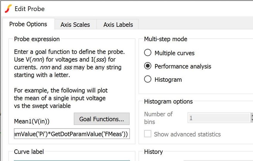
Output Capacitor Small-signal – Setup 2

 To calculate the output capacitor, we
 use an arbitrary-function probe with PeakToPeak(I(sns))/PeakToPeak(V(p))/(2*GetDotParamValue('Pi')*GetDotParamValue('FMeas'))

 the previous COSS equation. VDrain

 I(sns)

 p
 Coss

 Q
 NTHL040N65S3F_3p
 VDD
 Sin({VDD} {VMeas} {FMeas} 0 0)

 49
Output Capacitor Small-signal – Final Results These measurement are meet the datasheet results. As an example, for a drain-to-source equal to 400 V, we measured a COSS value of 142 pF in the figure. This value matches with 140 pF given in the datasheet. 50
Output Capacitor Small-signal – Schematic / 2nd Method

 In small-signal simulation, SIMetrix VDrain
 offers the possibility to sweep other I(sns)/(2*{Pi}*1Meg)

 parameters than frequency. Here, we Coss

 will set the frequency to 1 MHz and I(sns)
 sweep the drain-to-source dc voltage.

 We will use the following equation to Q
 400 AC 1 0
 VDD
 get COSS values :
 NTHL040N65S3F_3p

 =
 2 × ×V
 As the small signal is 1 V (0 dBV), it
 doesn’t count in the equation.

 51
Output Capacitor Small-signal – Setup / 2nd Method The sweep values are for VDD (drain-to-Source) voltage and the frequency is fixed. 52
Output Capacitor Small-signal – Results / 2nd Method

 2nd Method 1st Method

 53
Output Effective Capacitor - Definition The effective-capacitor value is The charging equation for the linear defined as the equivalent linear capacitor in this configuration is given capacitor storing the same amount of by: charge/energy with a voltage source − equal to breakdown voltage value and = 1 − × a 100-k series resistor to charge the Solving this equation to get COSS gives: output capacitor. = This value can be used to calculate the × − switching time in resonant topologies. 54
Output Effective Capacitor - Schematic
We use an arbitrary function to get the
Coss-VDS
COSS values and X-Y probe.
VDrain Y
The values for the resistor (RD) and
Coss_Effective
X the voltage source (VDD) are set with
p OUT parameters in the “Command
Windows” (F11). The values are
IC
0 RD
Coss
{RD}
time/(RD*ln(BVDSS/(BVDSS-V(p))))
100 k and 650 V respectively.
.Param RD=100k
Q {BVDSS}
VDD
NTHL040N65S3F_3p
.Param BVDSS=650
We set an initial condition for the
drain-to-source voltage using the “IC”
pseudo-component.
55Output Effective Capacitor - Results In the “Dynamic Characteristics” table, the effective output capacitor is given for a drain-to-source voltage equal to 400 V. On the side figure, we measure a COSS value equal to 1305 pF on the simulated curve. This matches with 1366 pF given in the specification. 56
Energy-related Output Capacitor - Definition

 The energy store in a capacitor is We use a current source to charge the
 expressed by the following equation: output.
 d = × × Here also, we use this formula in an
 And, the final energy for a constant arbitrary function to get the COSS value
 capacitor can be express by the directly.
 following equation: We use the integral function “SDT()” to
 1 2 calculate the numerator.
 =
 2 We set an initial condition for the
 We can extract the capacitor value: drain-to-source voltage using the “IC”

 2 0 × × pseudo-component.
 =
 2

 57
Energy-related Output Capacitor – Schematic and Results

 Coss-VDS
 VDrain
 Y

 2*SDT(V(p)*I(sns))/V(p)/V(p)
 X
 Coss_Energy

 I(sns)
 OUT

 p IC
 0

 Coss
 Q 1m
 IDD
 NTHL040N65S3F_3p

 In the “Dynamic Characteristics” table, the effective output capacitor is
 given for a drain-to-source voltage equal to 400 V. We measured a COSS value equal to 245 pF on the
 simulated curve above and this matches with 247 pF given in the specification.

 58
Charge-related Output Capacitor - Definition

 The charge store in a capacitor is We use almost the same schematic.
 expressed by the following equation: Here also, we use this formula in an
 = × arbitrary function to get the COSS value
 And, the final charge for a constant directly.
 capacitor can be express by the We use the integral function “SDT()” to
 following equation: calculate the numerator.
 = We set an initial condition for the
 We can extract the capacitor value: drain-to-source voltage using the “IC”

 pseudo-component.
 0 ×
 =

 59
Charge-related Output Capacitor – Schematic and Results

 Coss-VDS
 VDrain
 Y
 SDT(I(sns))/V(p)
 X
 Coss_Charge

 I(sns)
 OUT
 IC
 p 0

 Q Coss 1m
 IDD
 NTHL040N65S3F_3p

 60
Breakdown Voltage

 Simulation beyond the limits

61
Breakdown Voltage - Schematic

 The model gives the average values.
 The model is accurate inside the VDrain
 specification limits. Results outside XY Probe
 XY Probe

 specification limits are not warranted.
 But, the model can operate above the
 limits with relatively good accuracy
 and can predict values like the 1m

 average breakdown drain to source Q
 IDD

 voltage (BVDSS). NTHL040N65S3F_3p

 To simulate the breakdown voltage
 depending on the temperature, we will
 use a ramp current source up to 2 mA
 and plot the “off” characteristic

 62
Breakdown Voltage - Results

 We can note the leakage current
 varies with temperature. We can
 measure 23 µA, 33 µA and 254 µA for
 respectively -55°C, 25°C and 150°C
 die temperature at a drain to source
 voltage equal to 400 V. We see a big
 leakage current increase between
 25°C and 150°C.
 The drain to source breakdown voltage
 is equal to 648 V, 708 V and 781 V for
 respectively -55°C, 25°C and 150°C
 die temperature.

 63
Device Simulation Conclusion

64
So… Simulation is a much safer environment for testing the limits and above… All results in the data sheet can be obtained with those models. As testing conditions in the data sheet are ideal (or not realistic), Simulation can provide more realistic characteristics, Parameters or Values in real conditions can be obtained. Parameters not in the data sheet can also be obtained. Simulation models contain much more information than the data sheet. 65
Customer application

 Evaluate losses and junction temperature

66
Application - Description We will simulate a boost stage (for a The specification for the power stage solar inverter). is the following: To avoid long stabilization time, we will • Input voltage: 300 V, close the loop. We will use a type 3 • Output voltage: 420 V, compensator with a voltage-mode pulse width modulator. • Inductor current: 4 A, We will use arbitrary functions to • Inductor current ripple: 2 A, calculate losses in the diode, in the • Switching frequency: 100 kHz, MOSFET and the power to drive the MOSFET. • Case temperature: 90 °C, The “Per Cycle” measurement will be • Gate drive voltage: 10 V, used to get the average losses for • Gate series resistor: 8 . each cycle. 67
Application - Schematic
 Per Cycle Mean(PwrDrv) Per Cycle Mean(PwrDB) Per Cycle Mean(PwrTB)
 PwrDrv

 Losses Calculations IN Mean PwrDB
 IN Mean PwrTB
 IN Mean

 Averaging
 TIMING TIMING TIMING
 Clk Clk Clk
 PWM Comp
 UDrive UPWM UFeedBack
 Gate-Driver SinglePWM FeedBack-Type 3 ++
 Drive OUT
 DMin=0.05 DMax=0.8
 PWM Comp Comp Out
 SW PwrDB
 Duty Meas
 Zero=0 One=1 Tswr=10n Clk
 IN PwrDiode +VMin=0 VMax={VDrv}
 {CBoost} +Idrv=2 Rdrv=100m Ramp
 I(Sns)*V(P,N)

 Duty Clk Ramp Meas

 OUT
 CB

 {LBoost} IC=0
 {RBoost}

 I(sns)
 iLB

 RB
 LB
 OUT

 p
 n
 I(Sns)*V(P,N)
 PwrDrain
 Out
 Voltage
 Mode
 DB FFSB0665A_4p

 I(sns)
 {Vin}
 Vin
 PwrTB OUT
 p PWM Feedback

 Tcase

 Tj
 n

 TB-Tj
 FCH040N65S3_F155_5p Tj DB-Tj
 TB
 {Rgate} Tcase esrCout
 {RCout}
 RGate
 Iout

 Gate RT {Iout}
 n 1Meg
 Case
 p
 PwrDrv
 OUT {Ths}

 Heatsink temperature setting
 VHeatSink RD
 I(sns)
 1Meg +

 Drive Cout
 PwrGate
 {Cout}
 I(Sns)*V(P,N) IC={Vout*1.01}

 68
Application - Waveforms
Ideal Inductor = LB only
Real inductor = (LB+RB)//CB (with parasitics)
{CBoost}
CB
{LBoost} IC=0
{RBoost}
RB
LB
CB generate spikes on:
1) Output voltage
2) Input current
69Application – Losses & Junction Temperature For CB = 100 pF 70
Application – Losses & Junction Temperature vs CB
 The diode losses and the driving losses are not
 affected by CB values.

 We can measure the following values for the
 transistor as a function of the parasitic capacitor:
 CB=1 pF => 3.9 W losses & D(TJ)=1.1°C
 CB=10 pF => 4.0 W losses & D(TJ)= 1.2°C
 CB=100 pF => 4.9 W losses & D(TJ)= 1.4°C
 CB=1 nF => 14.0 W losses & D(TJ)= 4.1°C

 71
Application – Junction Temperature analysis

 There is a step in junction temperature
 waveform.
 This step is synchronous with turn on.

 So, there is a peak of power losses
 during turn on link to CB!

 Performance can be jeopardized by
 your inductor (parasitic capacitor)!

 72
Application – Optimization We keep the 100-pF inductor parasitic capacitor because this is a realistic value. The output power is equal to 1.2 kW. We obtain the following table after several trials using TO220 package for the diode and TO247 for the MOSFET. D Tj D TJ Drive MOSFET Diode Total MOSFET (TB) Diode (DB) MOSFET Diode Losses Losses Losses Losses FCH040N65S3 FFSP0465A 1,4 °C 7,3 °C 0,26 W 4,75 W 4,44 W 9,45 W FCH040N65S3 FFSP0665A 1,5 °C 10,0 °C 0,26 W 4,98 W 3,88 W 9,12 W FCH040N65S3 FFSP0865A 1,5 °C 4,1 °C 0,26 W 5,26 W 3,63 W 9,15 W FCH040N65S3 FFSP1065A 1,6 °C 3,9 °C 0,26 W 5,46 W 3,41 W 9,13 W FCH040N65S3 FFSP1265A 1,7 °C 3,7 °C 0,26 W 5,67 W 3,28 W 9,21 W FCH040N65S3 FFSP0665B 1,4 °C 13,5 °C 0,26 W 4,80 W 3,80 W 8,86 W FCH040N65S3 FFSP1065B 1,5 °C 5,4 °C 0,26 W 5,09 W 3,30 W 8,65 W FCH067N65S3 FFSP0665B 1,6 °C 13,6 °C 0,15 W 3,90 W 3,80 W 7,85 W FCH099N65S3 FFSP0665B 1,3 °C 13,6 °C 0,11 W 3,79 W 3,78 W 7,68 W FCH125N65S3R0 FFSP0665B 1,7 °C 13,6 °C 0,09 W 3,85 W 3,79 W 7,73 W FCH099N65S3 FFSP1065B 1,5 °C 9,4 °C 0,11 W 4,16 W 3,30 W 7,57 W The last configuration with 10 A SiC new generation diode (FFSP1065B) and 99 m EasyDrive SuperFET 3 (FCH099N65S3) gives less losses… But, a 10 A SiC diode for an average output current equal to 2.8 A could be consider oversized and, so, expensive. 73
Application Simulation Conclusion

74
So… Simulation gives a more realistic losses values than an estimated analytic function. Simulation can help to understand parasitic influences on an application schematic Running several configurations can help to find a better compromise between performances and cost. 75
Conclusion

76
Conclusion

 Physical and scalable models can
 really help designers to analyze
 components characteristics and
 applications performances.

 77
Thank you
 ? Question ?

78
You can also read