Touchscreen tags based on thin-film electronics for the Internet of Everything - Zenodo
←
→
Page content transcription
If your browser does not render page correctly, please read the page content below
Touchscreen tags based on thin-film
     electronics for the Internet of Everything
    Nikolaos Papadopoulos1, Weiming Qiu1, Marc Ameys1, Steve Smout1, Myriam
    Willegems1, Filip Deroo4, Jan-Laurens van der Steen2, Auke Jisk Kronemeijer2,
     Marco Dehouwer3, Alexander Mityashin1, Robert Gehlhaar1, and Kris Myny1
               1
                imec, Large Area Electronics, Leuven, 3001, Belgium
                 2
                   TNO/Holst Centre, Eindhoven, 5605, Netherlands
                        3
                         Cartamundi, Turnhout, 2300, Belgium
                     4
                      Cartamundi Digital, Drongen, 9031, Belgium

ABSTRACT
Capacitive touchscreens are increasingly widespread, featuring in mobile phones and tablets, as well as
everyday objects such as cars and home appliances. As a result, the interfaces are uniquely placed to
provide a means of communication in the era of the Internet of Everything. Here we show that commercial
touchscreens can be used as reader interfaces for capacitive coupled data transfer. The transfer of data
to the touchscreen is achieved using a 12-bit thin-film capacitive radio frequency identification tag
powered by a thin-film battery or a thin-film photovoltaic cell that converts light from the same screen.
The thin-film integrated circuit has a 0.8 cm2 on-chip monolithic antenna, employs 439 transistors, and
dissipates only 31 nW of power at a supply voltage of 600mV. The chip has an asynchronous data rate of
up to 36 bps, which is limited by the touchscreen readout electronics.

INTRODUCTION
In the Internet of Things (IoT), millions of devices are connected to cloud-based services by means of
different wireless communication protocols – including WiFi, Bluetooth Low Energy, and 4G/5G –
embedded on one or several silicon complementary metal-oxide-semiconductor (CMOS) chips. To enable
the transition from IoT to Internet of Everything (IoE), everyday items need to be equipped with wireless
communication chips that are low-cost and seamlessly integrated. Thin-film transistor (TFT) technology
on plastic substrates is a promising candidate to provide these IoE communication functions. The
technology can, in particular, provide flexible radio-frequency identification (RFID) tags1,2,3,4,5,6,7,8,9 that
can be concealed in numerous different objects such as paper tickets, official letters, certified documents,
and payment cards.

In proposed implementations of the IoE, a device/reader serves as a hub that connects everyday items
and objects via short-range communication (RFID) to the cloud. One initial potential scenario uses a TFT-
based near-field communication (NFC) chip5,7,10, as many people have access to phones and tablets
equipped with an accessible NFC reader. However, the number of connected NFC-enabled devices is still
relatively small, compared to the wide availability of touchscreens – and thus, with the right
communication technology, touchscreens could play a key role in delivering the IoE11.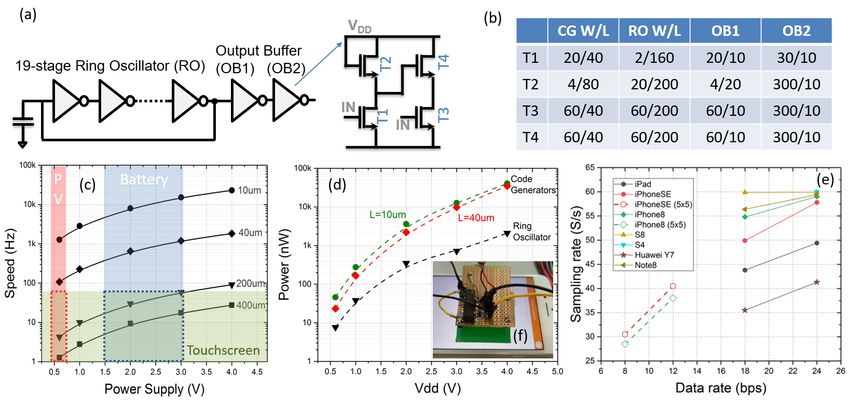
Although initially unforeseen12, a capacitive touchscreen can now be considered as a data communication
medium for non-human objects equipped with an identification chip. Data transfer occurs via the
capacitive antennas present on the chip and touchscreen. Capacitive communication offers many
advantages, including security (due to the very short communication range13), low cost (due to the
possibility of monolithically integrating antennas, no need for assembly and extra antenna substrate) and
widespread compatibility (due to the presence of capacitive touchscreens in everyday devices such as cars,
refrigerators, and coffee machines).

Novel forms of touchscreen interaction have already been demonstrated by combining Si-CMOS chips and
non-conventional off-the-shelf components such as bipolar transistors, mechanical relays, and tri-state
buffers13,14,15,16. Such non-conventional components are selected for their high off-state resistance
required to virtually switch off a touch event, mimicking to release a finger from the screen, limiting the
potential for a monolithic low-cost Si-CMOS solution. Metal-oxide TFT technologies exhibit a very low off-
current leakage20, which can be translated into a substantially high off-resistance interface to the screen.
In addition, the technology uses a self-aligned transistor architecture that has minimal capacitance and
could provide a monolithic solution for touchscreen communication.

We recently reported monolithically-integrated capacitive coupled thin-film RFIDs that used a custom-
built reader2,3. In the presented work, we report a TFT-based chip that can communicate electrically with
commercial capacitive touchscreens. Our chip is a capacitive RFID tag made from indium gallium zinc oxide
(IGZO) thin-film transistor technology on plastic substrates. It can be powered by a thin-film battery that
provides a continuous 1.5 V or thin-film photovoltaic cell that can generate up to 600 mV from the incident
light of a smartphone display. The tag system and communication method are tested using a range of
different touchscreens from a variety of brands, including Apple, Samsung, and Huawei.

TFT FABRICATION AND ELECTRICAL CHARACTERIZATION

2
(a)                    Electrode M3                       Electrode M3     (c)
                 Decoupling
                  dielectric
                                              Self-aligned TFT
                                                 L (µm)
           MIM-cap

                                  SD M2                        SD M2
                     SiNx
                                                     Gate M1
                                                      SiO2
                                                      IGZO
                                           Barrier
                                  Flexible substrate

     (b)                                                                      (d)

    Figure 1: Detailed information about the self-aligned metal-oxide TFT technology. (a) Device cross-
    section and (b) TFT transfer curves of 24 20 µm/40 μm self-aligned IGZO TFTs on 150 mm2 polyimide
    foil; (c) mobility distribution and threshold voltage distribution of various TFTs accross a 150mm2
    wafer; (d) Photos of the wafers (quarter of a GEN1 plate).

A self-aligned TFT architecture on a GEN1 (350mmx320mm) plastic substrate17 is used to fabricate the
Capacitive-touchscreen-tags (C-touch) tags (Fig. 1). Using a temporary glass carrier with a 15-μm-thick
polyimide film, a humidity barrier is deposited. Next, a thin layer IGZO is DC sputtered and patterned to
define the active semiconductor area. Then, to create a gate dielectric, a 200-nm-thick layer of SiO2 is
deposited using plasma-enhanced chemical vapour deposition (PECVD) at a temperature of 250°C.
Afterwards, 130-nm-thick MoCr is added as gate-metal. The dielectric and gate metal area is defined by
subsequent etching steps during the same photolitho-step. Next, 200-nm-thick SiNx is deposited using
PECVD in order to act as intermetal dielectric and so that hydrogen dopes the IGZO (decreasing its
resistance) in the areas not covered by the SiO2 gate dielectric. The contact holes for the source-drain (SD)
contacts are opened and MoCr/Al/MoCr is deposited and patterned to define the SD contacts. The stack
is passivated by a thick (around 2 μm) organic photo-exposable and curable interlayer/pixel definition
layer material from Tokyo Ohka Kogyo Co Ltd and 130-nm-thick MoCr is deposited and patterned. The last
step in the TFT process is a final anneal at 165°C. All process steps in the backplane process stay below a
thermal budget of 350°C.

The transfer characteristics and gate current of 24 TFTs with a width/length of 20 µm/40 µm are shown
in Fig.1b. The measurements have been obtained on various locations across the 150 mm² plate. The

3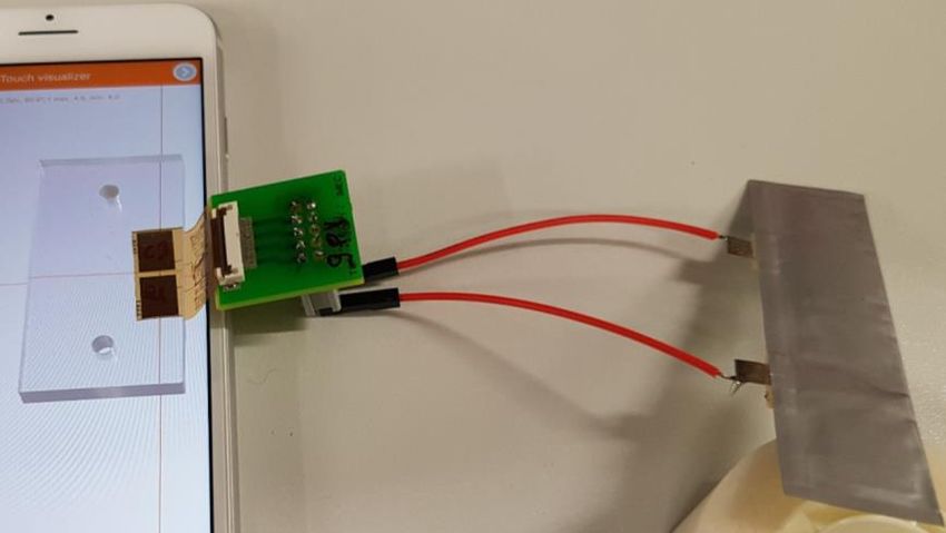
20/40 TFT is one most commonly used in our design and one of the smallest TFTs in the circuit blocks. The
extracted average charge carrier mobility and threshold voltage distributions are shown in Fig. 2c,d. The
median threshold voltage (VT ) is 0.65 V and the median mobility (μ) is 10.7 cm2/Vs. Moreover, the
standard deviation of VT is only 34 mV, the standard deviation of μ is 0.28 cm²/Vs across 150mm2 on the
plate. Self-aligned TFTs have negligible parasitic capacitance between gate and source-drain contacts, and
have been shown to be compatible with capacitive RFIDs2,3. Furthermore, modifying the thickness of gate
dielectric improves the input capacitance of the TFT: it results in 9 pF for a 50 nm thick gate dielectric, 6
pF for a 100 nm thick dielectric and 4 pF for a 200 nm thick dielectric for a 1500 µm /5 μm TFT. This is an
important parameter for enabling communication to a capacitive touchscreen.

THIN-FILM PHOTOVOLTAIC FABRICATION AND CHARACTERIZATION
Our thin-film photovoltaic (TFPV) has the following structure: Glass/indium tin oxide (ITO)/poly [N, N’-
bis(4-butylphenyl)-N,N’-bis(phenyl)-benzidine] (PolyTPD)/perovskite/Phenyl-C61-butyric acid methyl
ester (PCBM)/ZnO/Al (Figure 2(a)), where the nominal composition (composition calculated from the
precursor solution) of the perovskite is Cs0.1FA0.9Pb2.865Br0.135, whereby FA refers to formamidinium. The
average power conversion efficiency (PCE) after encapsulation is 13.5% ± 0.5%. A typical current density-
voltage (J-V) curve is shown in Fig. 2b, exhibiting a short-circuit current (Jsc) of 19.1mA/cm2, an open-
circuit voltage of 0.97V, and a fill factor of 76% under AM 1.5G spectrum. This device gives a steady PCE
of 13.7% when operating at 0.79V, which is maximum power point obtained from the J-V scan (inset of
Fig. 2b). The fabrication process is also compatible with flexible substrates18,19, offering monolithic
integration possibilities for the C-touch tag. A photo of the cells is shown in Fig. 5d.

The I-V curve and power output of one individual photovoltaic cell with 12.5 mm² active area placed on a
white colour screen of a Samsung Galaxy S8 phone is shown in Fig. 2c,d. Screen brightness is varied in
three levels (25%, 50% and 100%) and the voltage is swept from 0.9 V to -0.1 V and back with a delay time
of 0.02s between each measurement point. For 25% screen brightness the maximum achieved power is
~400nW at 0.6V. As expected, increasing the brightness of the screen increases the harvested power from
the photovoltaic, achieving 7μW at 100% brightness (as indicated by the phone). The phone was not fully
charged to emulate an average use case.

4
14.0                                                                   8
                              (c)                                                      (d)
                      12.0                                                                   7

                                                                                                 Output power (µW)
                              display brightness                                             6
                      10.0 100%
       Current (µA)

                                                                                             5
                       8.0
                                                                                             4
                       6.0    50%
                                                                                             3
                       4.0
                                                                                             2
                       2.0                                                                   1
                              25%
                       0.0                                                                   0
                             0.0    0.2   0.4      0.6   0.8   0.0   0.2   0.4   0.6   0.8
                                      Voltage (V)                      Voltage (V)

    Figure 2. Stack and characterization data of the perovskite solar cells. (a) Schematic of the
    perovskite solar cell structure; (b) a typical J-V curve of a single perovskite solar cell measured
    under AM 1.5G spectrum, with the inset showing the steady PCE when operating at 0.79 V; (c) I-V
    curve and (d) power output of one PV cell of 12.5 mm2 active area placed on a white color screen
    of a Samsung Galaxy S8 phone.

5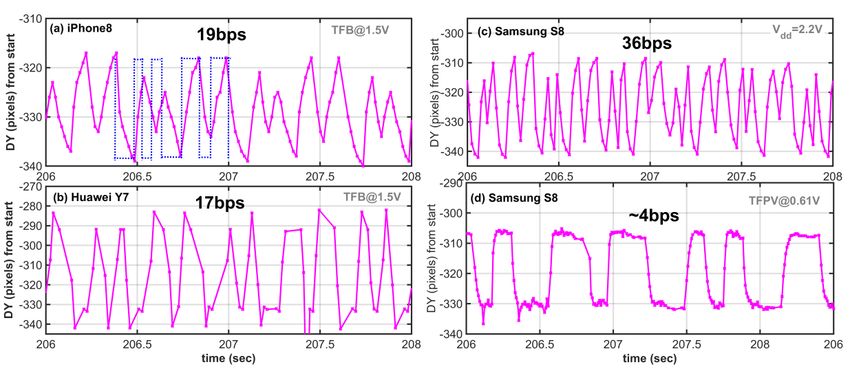
SYSTEM DESIGN CONSIDERATIONS

    Figure 3: Various high level C-touch system block diagrams. (a) Detailed schematics and (b) system
    blocks of C-touch tag and touchscreen reader.

The detailed schematic of the flexible C-touch tag, and a typical illustration of a touchscreen and its
electronics, is shown in Fig. 3a. The physical structure of the interface between the touchscreen and the
C-touch tag together with its main blocks is shown in Fig. 3b. The touchscreen’s transparent metal lines
are considered as the bottom plate of the capacitive coupler and the electrodes of the tag serve as top
plates. The glass of the touchscreen combined to the plastic or paper of the tag forms the dielectric of the
capacitive coupler. The roughness of different materials (glass/paper/plastic) adds air to the dielectric mix,
impeding the coupling of the tag to the touchscreen.

The complexity and diversity of modern touchscreens20,21 and their electronics22,23,24,25,26 is not captured
in Fig. 3; it focuses instead on the interface between the tag and the touchscreen and illustrates its main
properties. The power block of the TFT tag can be either a thin-film battery (TFB) or a thin-film
photovoltaic cell (TFPV). TFBs are available from 1.5 V to 4 V. Open circuit voltage of TFPVs have recently
improved reaching 0.8 V27,28 for organic cells, or around 1.2 V for perovskite solar cells29. The creation of
higher voltages using only TFPVs requires expensive and complicated fabrication methods to connect
TFPV cells in series forming a module. Another option would be to implement a DC-DC up-converter to
generate larger voltage levels. However, the high brightness of modern displays (>550 cd/cm2) is enough
to power the C-touch tag at 0.6 V (illustrated in Fig. 3), offering a monolithic solution for the full C-touch
system.

6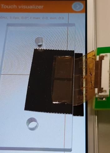
The main blocks of the flexible integrated circuit are a clock generator, a 12-bit code generator, a
modulator and the electrodes. The TFT sizing of the various block of the tag is shown in Fig. 4b. The clock
generator is a very critical block because it controls the data transmission rate to the touchscreen.
Experiments indicate that the touch event readout rate (sampling rate S/s) is limited to only 60 events/sec.
These sets of experiments (Fig. 4e) were performed on multiple touchscreens using various electrode sizes,
a discrete off-the-shelf-components built lab emulator (seen in Fig. 4f), and a special touch event app. The
same speed is confirmed by swiping a human-finger on a touchscreen using the same touch event
extraction app, setting a clock speed specification (Hz) to the clock generator as seen in Fig. 4c. To meet
the slow speed challenge the channel length of the 19-stage ring oscillator (RO), used as a clock generator,
is selected to be 200 µm and 400 µm, whereby a capacitor is included at the output of the RO for both
battery and PV power source. The 200 µm channel length design is selected because at 0.6 V the speed of
the 400 µm length is impractically slow (2.8 Hz). The power of the 200 μm RO measures 7.7 nW at 0.6 V.

    Figure 4: Technical data of the various circuit blocks of the c-touch tag. (a) Ring oscillators and
    inverter gate schematics; (b) table comprising TFT sizing of the different blocks; (c) speed scaling
    comparison of 4 different ring oscillator designs; (d) code generator power dissipation
    measurements data to the applied power supply voltage; (e) achieved sampling rate of the
    touchscreen for various phones and for various electrodes and data rates and (f) the c-touch
    emulator built from off-the-shelf silicon parts.

The 12-bit code generator (CG) with hard-wired memory embedding a bit-sequence 0101 0011 0110 is
designed using pseudo-CMOS logic gates30 with single supply operation2,3 employing 439 transistors. The
channel length of the logic gates is selected to be 40µm (Fig. 4b) to reduce total power dissipation of the
tag to prolong its lifetime in case of battery use or to reduce the footprint of the PV cell. A typical
commercially available TFB (0.5 mm thick) is providing 1.5 mAh/cm2 power at 3 V31. The CG is dissipating
~10 µW at 3 V yielding approximately 450 hours of continuous operation using a 1 cm2 TFB. Lowering the
power supply to 1 V multiplies the lifetime of the tag with more than an order of magnitude. At 600 mV
the CG dissipates less than 23 nW power, which results to total chip power dissipation of ~31nW, leading
to more than 9.5 years of continuous operation using a TFB. In addition, this low power value would enable

7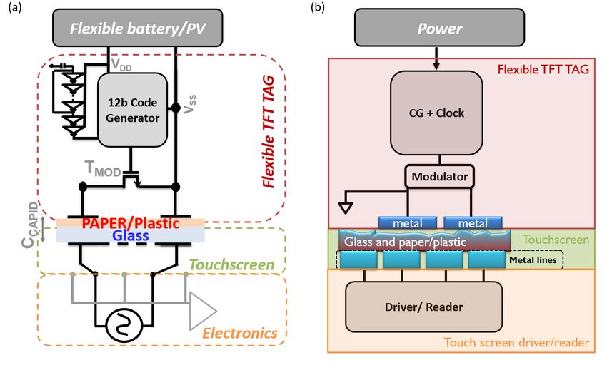
a monolithic solution whereby a TFPV can be directly integrated on top of a TFIC, requiring minimum
footprint. Figures 4c,d indicate that RO and CG are operational at 600 mV and prove that no serial
connection of multiple TFPV cells nor a DC-DC converter circuit is necessary.

The modulator of the tag is a large-sized TFT connected to the output of the CG after a 2-stage buffer
enhancing rise and fall times of the signal. The large W/L (1500/10) is selected to improve the modulation
and the distinction between a digital 0 and 1. Therefore, it facilitates the identification of the code from
the touchscreen and the application running on the device.

As mentioned earlier, the sizes of the electrodes have been evaluated using a developed lab touch
emulator (Fig. 4f). In Fig. 4e the need for 8x5 mm2 electrodes is illustrated to achieve 24 bps data rates.
Many different devices (iPad, iPhone SE, iPhone 8, Samsung S4, S8 and Note8, and Huawei Y7) were tested
using 1x1, 2x2, 5x5 and 5x8 (mm x mm) electrodes. Figure 4e indicates that larger-sized electrodes achieve
a better data transmission rate and improve the readout of the modulation of the tag at the touchscreen.
The mm-range size of the electrodes defines the size of the tag and provides large-area thin-film
electronics an important advantage compared to standard silicon CMOS technologies. Two electrodes are
used in the developed algorithm, whereby one electrode is permanently connected to ground, and the
other is connected to/disconnected from the ground depending on the bit-sequence 0101 0011 0110. A
‘1’ is creating a swipe event on the touchscreen from the permanently grounded electrode to the other.

8
C-TOUCH TAG EXPERIMENTAL RESULTS
(a) (b)
Interconnection
PCB Flexible Battery
TFT C-touch
Paper
(c) (d)
Power
TFT C-touch
PADS
CG+RO
Mod
PV
Electrodes
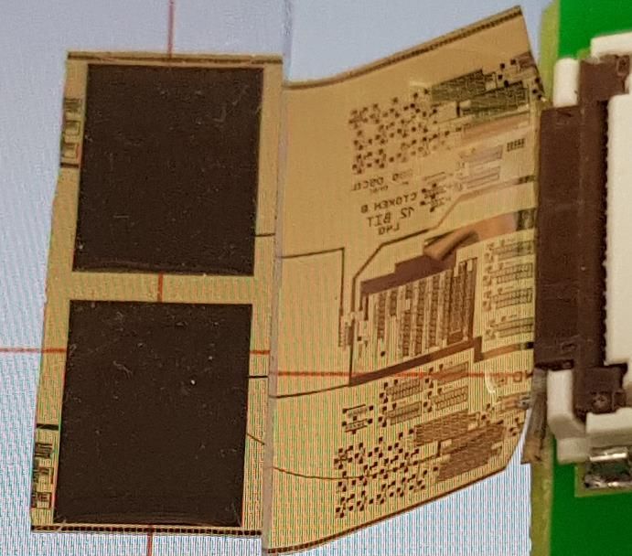
Figure 5: Photos of a flexible touchscreen tag connected to a flexible battery on an iPhone’s
touchscreen. (a) Without and (b) with paper in between; (c) a zoom-in to the delaminated flexible C-
touch tag itself with labels of the various parts and (d) the C-touch tag powered by a thin-film PV
from Samsung S8 display, whereby only the top-right cell is active.
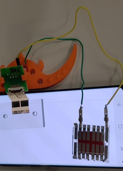
Figure 5a shows the setup used to connect the flexible TFT C-touch tag (with 0.8 cm2 electrodes) to a
commercially available flexible battery and Fig. 5d the C-touch tag connected to the developed TFPV. The
interconnection PCB is only present to make the physical connection of the two parts, no additional
electronics are present on the PCB. All the circuitry of Fig. 4 is integrated on the TFT C-touch tag. The
orange horizontal and vertical lines on the touchscreen are crossing at the precise point of the generated
touch event and are visible in Fig. 5. In Fig. 5c a zoom-in to the delaminated flexible C-touch tag without
rigid support carrier is shown, indicating the different circuit blocks.
Fig.6 shows the extracted touch event relocation data (DY=Y-Y0) as obtained from 3 commercial phones
without any change in their hardware or firmware settings. Y0 is the pixel’s y-axis coordinate of the first
touch event and Y the coordinate for the specific time. In Fig. 6a,b the DY data were received from
experiments where the C-touch tag was driven by 1.5 V TFB, as shown in Fig. 6a,b. In Fig.6 (a) the actual
9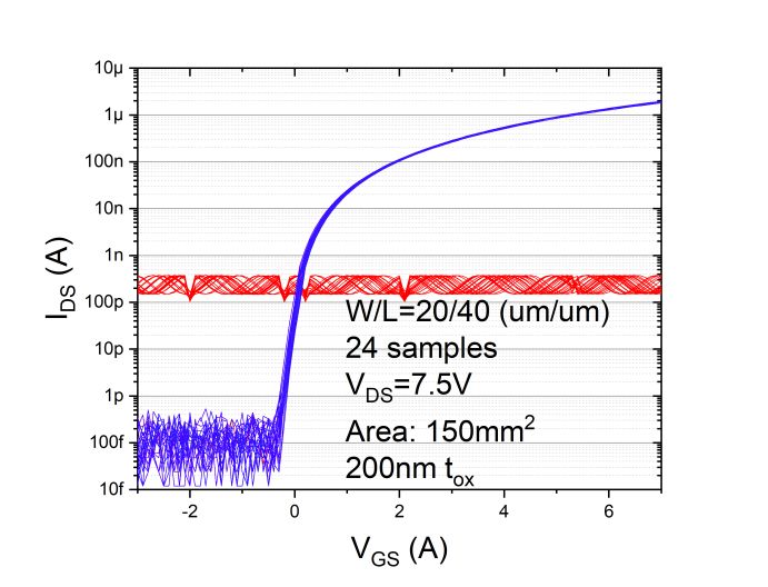
and 12-bit code sequence is indicatively illustrated with a blue dotted line to assist the understanding of
the DY data. The hard-wired bit-sequence of the flexible tag can be detected by using the prediscussed
touchscreen communication protocol. The 2 phones achieve similar transmission rates of 17-19bps but
differ in maximum relocation of the touch event (DYmax). The DYmax strongly depends on the resolution of
the display and the touchscreen readout chip. By comparing the plots in Fig.6, it can be concluded that
the sampling rates (pink dots) of the touchscreen electronics are not similar for all phones. The same
behaviour is shown in Fig. 4e, where similar experiments were performed using the lab C-touch emulator.

In a subsequent step, a gamecard paper (170 um thick) and a typical plastic screen protector have been
placed in between the tag and the touchscreens, as indicated in Fig. 6b (for the paper case). No differences
were observed either to the relocation DY or the speed of the data transmission rate to the touchscreen.

 Figure 6: Extracted location data from experiments of C-touch tag performed for various phones.
 (a) Received data on an iPhone 8 and (b) an Huawei Y7, powered by TFB at 1.5V; (c) received data
 on Samsung S8 touchscreens powered at 2.2 V and (d) powered by the TFPV at 0.61V, which is
 harvesting the emitted light of the smartphone display.

In Fig. 6c a faster data rate is achieved by driving the TFT C-touch tag at a higher supply voltage (2.2 V).
The obtained relocation data are a bit less clear compared to Fig. 6d, but still more clear compared to
other phones. Similar experiments of increasing data rates were performed on other phones as well,
whereby the bit-sequence was not always detectable. This implies that with the current state of
touchscreen technology, a universal upper limit in data rate should be used to ensure compatibility to a
wide range of phones. Obviously, one method to increase data rates with the proposed C-touch tags
would be a multitouch-multi-swipe event, whereby multiple electrodes can serve as input node. Another
method was proposed earlier in the literature13 by modifying the firmware of the touchscreens readout
hardware, obtaining up to 500 kb/s data transfer, paving the way for more complex data communication
to touchscreens, enabling a broader variety of applications.

Figure 6d plots the captured data by the touchscreen whereby the C-touch tag is powered by the TFPV.
The circuit and TFPV are connected by the same interconnect PCB and wiring as for the TFBAT. The PV cell
and tag have been placed on the smartphone display as shown in Fig. 5d. The brightness of the display of
the smartphone was regulated so that 610 mV is achieved by the TFPV. The tag achieves correct

10
transmission of 12-bit code to the touchscreen. The slow speed of 4 bps is due to the ring oscillator
integrated on the tag. Faster speeds can be achieved, integrating a faster ring oscillator as shown from
Fig. 4c.

CONCLUSIONS
We have reported capacitive coupled data transfer using a flexible C-touch chip (a capacitive RFID tag)
based on thin-film transistor technologies and commercial touchscreens as a reader interface. The tag can
be integrated with a thin-film battery that provides a continuous 1.5 V. Alternatively, it can be connected
to a thin-film, foil-compatible photovoltaic cell that has an active area of only 12.5 mm2; the photovoltaic
cell can generate 600 mV from the incident light of a smartphone display. The C-touch tag can achieve
data transfer rates of up to 36 bps at a supply voltage of 2.2 V provided by external power supply or
battery. This is in the range of detectable sampling rates of current pristine touchscreen readout
electronics. The power consumption of the tag was four times lower than the previously reported 12-bit
code generator2 and dissipated only 31 nW at a 600 mV supply. Our C-touch tag technology could
potentially be implemented on 4.5 billion mobile phones worldwide32 and the extra touchscreen-enabled
devices (cars, home appliances, smart surfaces, tables, etc) in the near future without additional costs for
the users.

REFERENCES
1.       Cantatore, E. et al. A 13.56-MHz RFID System Based on Organic Transponders. IEEE J. Solid-State
Circuits 42, 84–92 (2007).

2.      Papadopoulos, N. et al. 2-D Smart Surface Object Localization by Flexible 160-nW Monolithic
Capacitively Coupled 12-b Identification Tags Based on Metal-Oxide TFTs. IEEE Trans. Electron Devices 1–
7 (2018) doi:10/gfb5tz.

3.      Papadopoulos, N. et al. 1cm2sub-1V Capacitive-Coupled Thin Film ID-Tag using Metal-oxide TFTs
on Flexible Substrate. in 2018 International Flexible Electronics Technology Conference (IFETC) 1–2
(2018). doi:10.1109/IFETC.2018.8583891.

4.        Hung, M.-H. et al. Ultra Low Voltage I-V RFID Tag Implement in a- IGZO TFT Technology on
Plastic. IEEE Int. Conf. RFID 5 (2017).

5.      Myny, K. The development of flexible integrated circuits based on thin-film transistors. Nat.
Electron. 1, 30–39 (2018).

6.     Yang, B.-D. A Transparent Logic Circuit for RFID Tag in a-IGZO TFT Technology. ETRI J. 35, 610–
616 (2013).

7.     Myny, K., Tripathi, A. K., van der Steen, J.-L. & Cobb, B. Flexible thin-film NFC tags. IEEE Commun.
Mag. 53, 182–189 (2015).

8.       Klauk, H., Zschieschang, U., Pflaum, J. & Halik, M. Ultralow-power organic complementary
circuits. Nature 445, 745–748 (2007).

11
9.      Ke, T.-H. et al. Scaling down of organic complementary logic gates for compact logic on foil. Org.
Electron. 15, 1229–1234 (2014).

10.     Myny, K. et al. 15.2 A flexible ISO14443-A compliant 7.5mW 128b metal-oxide NFC barcode tag
with direct clock division circuit from 13.56MHz carrier. in 2017 IEEE International Solid-State Circuits
Conference (ISSCC) 258–259 (IEEE, 2017). doi:10.1109/ISSCC.2017.7870359.

11.     Villar, N. et al. Project Zanzibar: A Portable and Flexible Tangible Interaction Platform. in
Proceedings of the 2018 CHI Conference on Human Factors in Computing Systems - CHI ’18 1–13 (ACM
Press, 2018). doi:10/gfsjqx.

12.    JOHNSON, E. A. Touch Displays: A Programmed Man-Machine Interface. Ergonomics 10, 271–
277 (1967).

13.     Vu, T. et al. Capacitive Touch Communication: A Technique to Input Data through Devices’ Touch
Screen. IEEE Trans. Mob. Comput. 13, 4–19 (2014).

14.    Coni, P., Perbet, J.-N., Augros, L., Abadie, J. C. & Sontag, Y. 6.1: A New Application of a Touch
Screen Display for Data Transfer. SID Symp. Dig. Tech. Pap. 46, 37–40 (2015).

15.     Yu, N.-H. et al. TUIC: enabling tangible interaction on capacitive multi-touch displays. in
Proceedings of the 2011 annual conference on Human factors in computing systems - CHI ’11 2995 (ACM
Press, 2011). doi:10/cpm7js.

16.     Kubitza, T., Pohl, N., Dingler, T. & Schmidt, A. WebClip: a connector for ubiquitous physical input
and output for touch screen devices. in Proceedings of the 2013 ACM international joint conference on
Pervasive and ubiquitous computing - UbiComp ’13 387 (ACM Press, 2013). doi:10/gfsjqz.

17.    Kronemeijer, A. J. et al. P-127: Dual-Gate Self-Aligned IGZO TFTs Monolithically Integrated with
High-Temperature Bottom Moisture Barrier for Flexible AMOLED. SID Symp. Dig. Tech. Pap. 49, 1577–
1580 (2018).

18.     Qiu, W. et al. High efficiency perovskite solar cells using a PCBM/ZnO double electron transport
layer and a short air-aging step. Org. Electron. 26, 30–35 (2015).

19.     Qiu, W. et al. An Interdiffusion Method for Highly Performing Cesium/Formamidinium Double
Cation Perovskites. Adv. Funct. Mater. 27, 1700920 (2017).

20.     Xiao, F., Wang, Z., Ye, N., Wang, R. & Li, X.-Y. One More Tag Enables Fine-Grained RFID
Localization and Tracking. IEEEACM Trans Netw 26, 161–174 (2018).

21.    Walker, G. A review of technologies for sensing contact location on the surface of a display:
Review of touch technologies. J. Soc. Inf. Disp. 20, 413–440 (2012).

22.     Barrett, G. Projected-Capacitive Touch Technology. 6 doi:10/gfsjq5.

23.    Jang, Y.-S. et al. P-181: A Charge-Share-Based Relative Read-Out Circuit for Capacitance Sensing.
SID Symp. Dig. Tech. Pap. 41, 1937–1939 (2010).

24.     Hamaguchi, M., Nagao, A. & Miyamoto, M. 12.3 A 240Hz-reporting-rate 143×81 mutual-
capacitance touch-sensing analog front-end IC with 37dB SNR for 1mm-diameter stylus. in 2014 IEEE

12
International Solid-State Circuits Conference Digest of Technical Papers (ISSCC) 214–215 (2014).
doi:10/gftpsk.

25.     Jun, J. et al. In-Cell Self-Capacitive-Type Mobile Touch System and Embedded Readout Circuit in
Display Driver IC. J. Disp. Technol. 12, 1613–1622 (2016).

26.    An, J., Jung, S., Hong, S. & Kwon, O. A Highly Noise-Immune Capacitive Touch Sensing System
Using an Adaptive Chopper Stabilization Method. IEEE Sens. J. 17, 803–811 (2017).

27.   Peumans, P., Yakimov, A. & Forrest, S. R. Small molecular weight organic thin-film
photodetectors and solar cells. J. Appl. Phys. 93, 3693–3723 (2003).

28.     Cui, Y. et al. Over 16% efficiency organic photovoltaic cells enabled by a chlorinated acceptor
with increased open-circuit voltages. Nat. Commun. 10, 2515 (2019).

29.     Tress, W. et al. Interpretation and evolution of open-circuit voltage, recombination, ideality
factor and subgap defect states during reversible light-soaking and irreversible degradation of
perovskite solar cells. Energy Environ. Sci. 11, 151–165 (2018).

30.     Huang, T.-C. et al. Pseudo-CMOS: A Design Style for Low-Cost and Robust Flexible Electronics.
IEEE Trans. Electron Devices 58, 141–150 (2011).

31.     CP series lithium manganese primary pouch cells High capacity (5mm), Thin (1 mm) to Ultrathin
(0.5 mm) non-rechargeable Lithium Cells from GM Battery and PowerStream.
https://www.powerstream.com/thin-primary-lithium.htm.

32.     Number of mobile phone users worldwide 2015-2020. Statista
https://www.statista.com/statistics/274774/forecast-of-mobile-phone-users-worldwide/.

ACKNOWLEDGEMENTS
The authors would like to thank the process engineers of Holst Centre's GEN1 Pilot Line for fabricating
the circuits presented in this paper. This work has received funding from the European Research Council
(ERC) under the European Union's Horizon 2020 research and innovation program under grant
agreement No 732389 (CAPID project) and No 716426 (FLICs project). Part of this work is financed
through the Flexlines project within the Interreg V-programme Flanders-The Netherlands, a cross-border
cooperation programme with financial support from the European Regional Development Fund, and co-
financed by the Province of Noord-Brabant, The Netherlands. W. Q. would like to thank the financial
support of the postdoctoral researcher grant (12Z4618N) received from Research Foundation Flanders
(FWO), Belgium.

AUTHOR CONTRIBUTIONS STATEMENT
N.P. and K.M. conceived conducted and analyzed the experiment(s), M.A. conceived experiments, R.G.
and W.Q. conducted the TFPV analysis and fabrication, F.P. developed the apps, S.S. and M.W. A.K and J-

13
L.S conducted the fabrication, M.D. and A.M. conceived the applications. All authors reviewed the
manuscript.

METHODS:
“The data that support the plots within this paper and other findings of this study are available from the
corresponding author upon reasonable request”.

14
You can also read