Zero Latency Multiplexing I/O for ASIC Emulation
←
→
Page content transcription
If your browser does not render page correctly, please read the page content below
Application Note: Xilinx FPGAs

                                    Zero Latency Multiplexing I/O for
                                    ASIC Emulation
XAPP1217 (v1.0) March 17, 2015      Author: Luis Bielich

Summary
           This application note provides a method for FPGA emulation platforms to communicate
           multiple signals over one I/O or I/O differential pair to another FPGA. This multiplexing method
           serializes data up to 800 Mb/s without introducing any additional cycles of latency to the user
           who is running at a slower rate.

Overview
           FPGAs are commonly used for emulation systems of complex ASICs. Because the ASIC logic
           outnumbers the logic in an FPGA, multiple FPGAs are required and the ASIC logic is distributed
           between the multiple FPGAs. The communication between FPGAs is a result of the ASIC being
           subdivided, so it is possible for hundreds or even thousands of logical signals to be needed to
           cross from one FPGA to the next. Even with the largest FPGAs, there might not be enough
           general purpose I/O to send all of the signals from one FPGA to another. Serializing a parallel
           path from one FPGA to another is a common method to enable one I/O to account for multiple
           signals going from one FPGA to another. This method is called Multiplexing I/O in this
           application note. Figure 1 shows the serialization concept.

XAPP1217 (v1.0) March 17, 2015                www.xilinx.com                                              1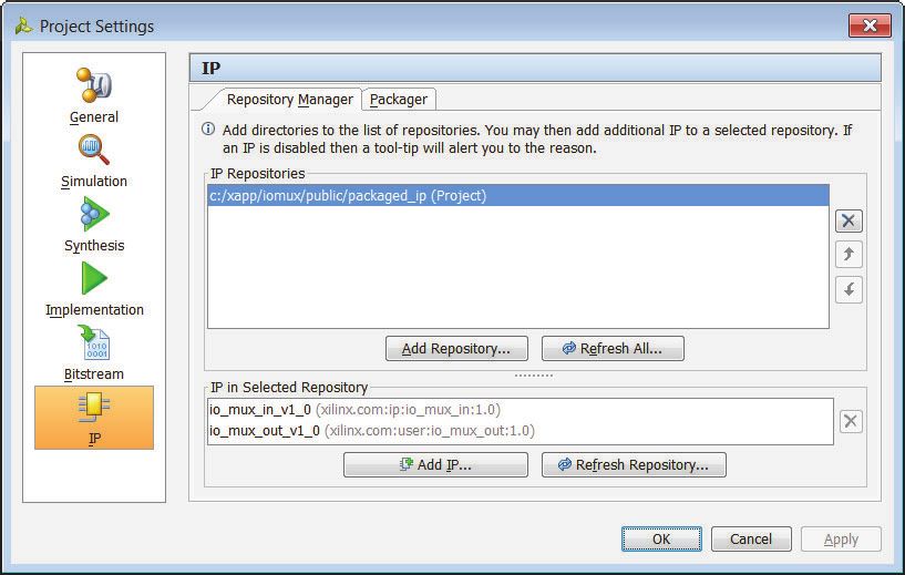
Overview
X-Ref Target - Figure 1
7UDQVPLW)3*$ 5HFHLYH)3*$
$>@
$>@
$>@
$>@
$>@
$>@
$>@
$>@
'H08;
08;
$>Q@ $>@ $>@ $>@ $>@ $>@ $>@
$>@
$>@
$>@
$>@
$>Q@
$>Q@
;BB
Figure 1: Multiplexing I/O Conceptual Block Diagram
Although serializing appears as the obvious solution for getting multiple signals over one I/O,
this application note focuses on getting all the signals over in less than one parallel clock cycle,
as in zero latency. The benefit of getting all of the signals over in less than one clock cycle is
that the ASIC logic does not need to be modified as long as there are no timing bottlenecks.To
get all of the bits over in one clock cycle, the effective multiplexed ratio must be reduced. For
example, if the serial bit time is 32x the parallel frequency, the effective multiplexing capability
must be less than 32x. The reasoning behind the reduction in the effective multiplexed ratio is
shown in Figure 2, which displays how the first bits transmitted are received before the next
parallel clock cycle, allowing for bits to be utilized by the design before the subsequent parallel
clock edge. The bits showing up after the parallel clock are referred to as clipped bits in the
context of this document, and they are the bits that are discarded. In Figure 2, bits A[31:21] are
considered clipped bits, while bits A[20:0] are the valid bits yielding the effective multiplexing
ability of 21 to 1 for every I/O or I/O differential pair.
X-Ref Target - Figure 2
&/2&.B',9
&/.B''5
3DUDOOHO'DWD $>
@ $>
@ $>
@ %>
@
7UDQVPLW6HULDO'DWD $>@ $>@ $>@ $>@ $>
@ $>@ $>@ $>@ $>@ $>@ $>@ $>@ $>
@ $>@ $>@ %>@
5HFHLYHG6HULDO'DWD $G>@ $G>@ $G>@ $G>@ $G>@ $G>@ $G>@ $G>
@ $G>@ $G>@
'LJLWDO/DWHQF\%RDUG'HOD\3DFNDJH,'(/$< 9DOLG%LWV
;BB
Figure 2: Multiplexing I/O Conceptual Waveform
XAPP1217 (v1.0) March 17, 2015 www.xilinx.com 2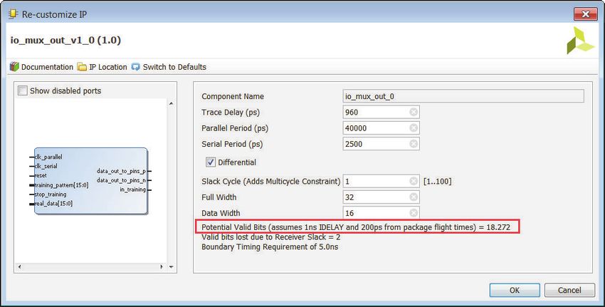
Hardware Description

          As illustrated in Figure 2, the digital latency, trace delay, package delay, and IDELAY delay
          subtract from the valid bits. The more total delay, the less valid bits available and the more bits
          are clipped. Therefore, minimizing these delays is always encouraged. Skew between the
          parallel clocks on both FPGAs also affects the effective valid bits. When possible, reduce the
          skew of the parallel clock domains.

Hardware Description
          There are two designs provided in this application note, each packaged as a piece of custom IP
          for the Vivado® Design Suite:

          •                   Output MUX transmitter
          •                   Input DeMUX receiver

          Transmitter
          The transmitter polls the parallel clock waiting for a rising edge. After a rising edge is detected,
          the transmitter starts transmitting the user data at the serial rate with the ODDR primitive. In
          Figure 2, the user data is referred to as the valid bits. The transmitter transmits the valid bits
          first and the clipped bits later. The clipped bits are assigned to zero. The number of valid bits
          transmitted is designated by the effective multiplexing ratio, which is designated by the
          DATA_WIDTH parameter. The total number of bits transmitted in a parallel clock is designated
          by the FULL_WIDTH parameter. The difference between the FULL_WIDTH and the DATA_WIDTH
          results in the clipped bits, as shown in Figure 3.
          X-Ref Target - Figure 3

                                        3DUDOOHO'RPDLQ
                                                                                        &RQWURO/RJLF


                                                    9DOLG
                                                    %LWV

                                                                                                  2''5

                                                              'DWD:LGWK

                                                   &OLSSHG
                                                     %LWV      )XOO:LGWK

                                                                                                 6HULDO'RPDLQ
                                                                                                           ;BB

                                                      Figure 3:   Transmit Multiplexer Block Diagram

XAPP1217 (v1.0) March 17, 2015                                    www.xilinx.com                                             3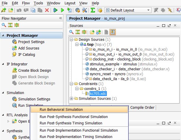
Hardware Description

          Receiver
          The receiver passes the data through an IDELAY primitive before getting captured with the IDDR
          primitive. After the IDDR, the valid bits are deserialized into the parallel domain while the
          clipped bits are discarded and never presented to the user. To determine which bits are valid or
          clipped, a calibration stage is needed upon the release of reset. Figure 4 shows a block diagram
          of the receiver design.
          X-Ref Target - Figure 4

                                              6HULDO'RPDLQ                                 3DUDOOHO'RPDLQ

                                                                                               &DOLEUDWLRQ
                                                                            &RQWURO/RJLF        %ORFN

                                                  ,'(/$<      ,''5                                      8VHU'DWD

                                                                                                        ;BB

                                                       Figure 4:     Receiver DeMUX Block Diagram

          Calibration
          The purpose of the calibration engine is to perform these two functions:

          •                   Center the IDELAY taps to capture at the center of the valid eye
          •                   Find the appropriate cycles where valid bits are located

          The receiver must calibrate upon each power cycle, or after reset is released. Although the
          receiver is performing the calibration, the transmitter needs to be placed in calibration mode to
          provide the training pattern to the receiver. When the transmitter comes out of reset, it should
          be placed in a training mode where the user data is not passed in by keeping the stop_training
          input deasserted. Instead, the training data from the training_pattern input is transmitted.

          Note: The training_pattern should be kept as a static value, but is left as an input to accommodate for
          dynamic training patterns.

          After the reset to the receiver is released, the receiver is in a calibration mode. The receiver
          comes out of calibration after the training pattern is detected. During receive calibration, the
          IDELAY taps are swept to find the center of the capture eye. After the center of the data valid
          window is found and the data matches the training pattern, the IDELAY taps are placed in the
          center of the capture eye and the calib_comp signal asserts. The calib_comp signal from the
          receiver should let the transmitter know that it is ready to come out of calibration. When
          multiple I/Os are used to multiplex I/Os, it is possible to leave all the transmitters in training

XAPP1217 (v1.0) March 17, 2015                                 www.xilinx.com                                             4
Partitioning the Design
mode until all of the receivers have completed calibration. Figure 5 shows the sequencing of
the control and status signals for the transmitter and receiver.
X-Ref Target - Figure 5
75$160,77(5
3DUDOOHO&ORFN
UHDGBGDWD $ %
UHVHW
LQBWUDLQLQJ
VWRSBWUDLQLQJ
5(&(,9(5
FDOLEBFRPSO
GHOD\BORFNHG
UHVHW
;BB
Figure 5: Control and Status Signal Sequencing
Partitioning the Design
You must decide where the ASIC logic is partitioned across FPGAs. It is recommended for these
boundaries to have lower levels of logic to achieve timing closure. In Figure 6, this refers to the
blocks labeled User Logic. The User Logic code remains logically equivalent because it would be
in the ASIC. The timing boundaries between the User Logic and the Serializer or Deserializer are
tighter than the parallel clock period, which is why you should choose boundaries with lower
levels of logic.
X-Ref Target - Figure 6
7UDQVPLWWHU 5HFHLYHU
8VHU/RJLF 6HULDOL]HU 2''5 ,''5 'HVHULDOL]HU 8VHU/RJLF
7UDLQLQJ 7UDLQLQJ
3DWWHUQ
*HQHUDWRU
&RQWUROV
2XWSXW08; ,QSXW'H08;
/HJHQG
6HULDO 3DUDOOHO
'RPDLQ 'RPDLQ
;BB
Figure 6: Example of x16 User Data Width System
XAPP1217 (v1.0) March 17, 2015 www.xilinx.com 5Hardware Requirements and Considerations
Hardware Requirements and Considerations
The list below provides the hardware requirements and considerations for using this application
note:
• Parallel Clocks are System Synchronous and the Same Frequency
• Serial Clocks are System Synchronous and the Same Frequency
• Serial Clock and Parallel Clock Should be Synchronous to Each Other
• I/O Data Valid Capture Window of Six IDELAY Taps
• Running Potential Valid Bits Calculation
• Special Considerations for Timing Constraints
Parallel Clocks are System Synchronous and the Same Frequency
The parallel clock is the clock domain containing the bus of the signal that will be serialized.
This clock must be derived on both FPGAs from the same oscillator. This design does not
account for PPM difference from different clock domains. In other words, both FPGAs must be
system synchronous. The frequency should also be the same on both FPGAs.
Serial Clocks are System Synchronous and the Same Frequency
The relationship between the serial clocks on both FPGAs must have similar requirements as the
relationship between the parallel clocks. The serial clocks must originate from the same
oscillator so there are no PPM differences, and the frequencies must be the same.
Serial Clock and Parallel Clock Should be Synchronous to Each
Other
The relationship between the serial clock and the parallel clock must be synchronous. Use the
same MMCM to generate both the clocks. This reduces the uncertainty between the serial clock
and the parallel clock and allows for better timing closure.
I/O Data Valid Capture Window of Six IDELAY Taps
IBIS simulations are required to account for signal integrity. A data valid window of at least six
IDELAY taps is required. Refer to the targeted device data sheet to find the delay of one IDELAY
tap. For 7 series FPGAs, one IDELAY tap is 78 ps with a 200 MHz reference clock to the IDELAY
controller, and 52 ps with a 300 MHz reference clock. If a 78 ps tap is used, a data valid window
of 78 ps x 6 = 468 ps is required. The calibration logic calibrates only once during start-up, so
a controlled environment is recommended. Remember to include a BUFG duty cycle distortion
(DCD) of 200 ps as part of the data valid window. Because the serial clock is running fast, static
timing is not required on the I/O. Instead, the calibration logic accounts for finding the center
of the eye.
XAPP1217 (v1.0) March 17, 2015 www.xilinx.com 6Hardware Requirements and Considerations
Running Potential Valid Bits Calculation
Prior to running anything on hardware, you are required to run a calculation of the potential
valid bits. This tells you what is possible to transmit in one parallel clock cycle given the serial
transmit rate. The details behind the calculation are described in Steps for Determining Actual
MUX Ratio.
Special Considerations for Timing Constraints
Transmitter
Referring back to Figure 2, the timing constraints from the parallel clock domain into the serial
clock domain (and vice versa) are going to be one serial clock cycle. Because the serial clock is
operating at a high frequency, it is desirable to relax the timing requirement. This can be done
on the transmitter by increasing the SLACK_CYCLE option in the IP. This allows the ability to
multicycle the constraints from the parallel domain into the serial domain of the datapath by
the number indicated by the SLACK_CYCLE parameter. Increasing SLACK_CYCLE reduces the
number of effective valid bits transferred. Figure 7 illustrates how increasing SLACK_CYCLE
relaxes the constraints while reducing the effective valid bits.
X-Ref Target - Figure 7
3DUDOOHO&ORFN
6HULDO&ORFN
3DUDOOHO'DWD $>
@ $>
@ $>
@ %>
@
7UDQVPLW6HULDO'DWD $>@ $>@ $>@ $>@ $>@ $>@ $>@ $>@ $>@ $>@ $>@ $>
@ %>@
6ODFN&\FOHV
5HFHLYHG6HULDO'DWD $G>@ $G>@ $G>@ $G>@ $G>@ $G>@ $G>@ $G>@ $G>
@ $G>@
'LJLWDO/DWHQF\%RDUG'HOD\3DFNDJH,'(/$< 9DOLG%LWV
;BB
Figure 7: SLACK_CYCLE Enabling Multicycle of Parallel Domain to Serial Domain in Transmitter
Receiver
Similar to the transmitter, the receiver is able to reduce the timing requirement on the user
boundary. This is done by maintaining the same parallel and serial clock frequencies and
reducing effective multiplexing ratio. When this is done, the data can be captured faster and is
XAPP1217 (v1.0) March 17, 2015 www.xilinx.com 7Steps for Determining Actual MUX Ratio
waiting for the rising edge of the parallel clock for multiple serial clock cycles. The slack cycle in
Figure 8 shows how a multicycle constraint can relax this constraint.
X-Ref Target - Figure 8
3DUDOOHO&ORFN
3DUDOOHO&ORFN
N
6HULDO&ORFN
6HULDO&ORFNN
3DUDOOHO'DWD
3DUDOOHO'DWD
D $>
@ $>
@ $>
@ $>
@
$>
@ %>
@
%>
@
7UDQVPLW6HULDO'DWD
7UDQVPLW6HULDO'DW $>@ $>@ $>@
$>@ $>@
$ @@ $>@
$>@ $>
@ $>@
$>@ $>@
$>@ $>@
$>@ $>@
$>@ $>@
$>@ $>@
$>@ $>@
$>@ $>@
$>
@ $>
@
$>@ %>@
$>@ > %>@
6
6WDFN&\FOHV
F
5HFHLYHG6HULDO'DWD
5HFHLYHG6HULDO'DWD
W $G>@ $$G$>>@
>@@ $GG>@
@
G>@ >@ $
$GG>@
>@ $GG>@
>@ $GG>@
>@ $$GG>@
>@ $G $G>
@
6ODFN
'LJLWDO/DWHQF\%RDUG'HOD\3DFNDJH,'(/$<
'LJLWDO/DWHQF\%RDUG'HOD\3DFNDJH,'(/$<
D F D \ D ' 9DOLG%LWV
&\FOH
;BB
Figure 8: Reducing Valid Bits to Increase Receive Timing Margin
Steps for Determining Actual MUX Ratio
Now that the concept of additional timing margin is introduced for both the receiver and
transmitter, it is possible to calculate how many actual valid bits are expected for a given board
configuration. The actual valid bits per MUX/DeMUX determine how many I/Os are necessary to
go between FPGAs. Multiple instances of the MUX/DeMUX result in the total number of signals.
The calculations are require the following information:
• Ratio between serial clock and parallel clock domain.
• Board trace delay.
• Package flight times.
• IDELAY delay with zero taps (from timing analyzer). Usually around 1 ns of delay.
• Digital delays from design:
° Output has two serial clock cycles of latency.
° Input has four serial clock cycles of latency.
• Desired slack on transmit and receive end.
• Clock skew of the parallel clocks on both FPGAs.
Follow steps 1 through 4 to determine the actual multiplexing ratio with the appropriate slack
on the input and output.
Step 1: Calculate Potential Valid Bits
Equation 1 shows the calculation for the potential (not actual) number of valid bits (PVB):
PCP – IODd – Id – BTd – PFT – PCS
----------------------------------------------------------------------------------------------------- = PVB Equation 1
SBT
XAPP1217 (v1.0) March 17, 2015 www.xilinx.com 8Steps for Determining Actual MUX Ratio
where:
PCP = Parallel clock period
IODd = Input and output digital delays
Id = IDELAY delay
BTd = Board trace delay
PFT = Package flight times
PCS = Parallel clock skew
SBT = Serial bit time
PVB = Potential valid bits
The IP customization window also performs the calculation for you within the IP window, as
shown in Figure 9. The only limitations are that the IDELAY is fixed at 1 ns, the package flight
times are fixed at 200 ps, and the clock skew is assumed to be zero. To work around the
limitations, the additional timing can be allocated in the Trace Delay option as shown in
Figure 9.
X-Ref Target - Figure 9
;B
B
Figure 9: Potential Valid Bits Calculation within the IP Customization Window
Step 2: Decide if the Serial Clock Period is a Timing Bottleneck
Now that the total number of potential valid bits is calculated, it is up to you to decide if a serial
clock period is going to be a reasonable timing constraint between the parallel clock and the
serial clock. If the serial clock period is reasonable, total potential valid bits can be used as the
user data width. If a serial clock period is too tight, it is possible to relax the constraint by
proceeding to step 3.
Step 3: Relaxing Transmitter Constraint
If timing margin is needed at the transmit end, it is possible to relax the timing at the expense
of losing a resolution of two valid bits. For example, relaxing the constraint by two extra serial
clock cycles results in a loss of four valid bits. Each serial clock cycle of margin loses two valid
bits of multiplexing. The timing constraints are already added into the IP, and the RTL is also
XAPP1217 (v1.0) March 17, 2015 www.xilinx.com 9Steps for Determining Actual MUX Ratio
modified to allow for the additional time for the parallel data to settle into the serial domain.
The SLACK_CYCLE parameter of the IP needs to be increased to allow for more slack. A
SLACK_CYCLE of one does not increase slack and remains at the serial clock requirement.
Increasing SLACK_CYCLE to one adds one serial clock cycle of slack and consequently loses two
valid bits. If the RTL is directly used (instead of the IP), it is necessary to add the appropriate
timing exceptions between the serial and parallel clock domain; otherwise, the IP does not
function.
Step 4: Relaxing Receiver Timing
Similar to the transmitter, the receiver timing can also be relaxed at the expense of valid bits.
This is also done within the IP with the SLACK_CYCLE option in the IP, which removes two valid
bits for every additional SLACK_CYCLE. A difference between the transmitter and the receiver
design is the effect of the SLACK_CYCLE option. For the receiver design, the SLACK_CYCLE
option only changes the constraints for the IP and does not affect the source code. In the
transmitter, the constraints and source code are affected by the SLACK_CYCLE option.
Example of Calculating Actual MUX Ratio
For this example, the parallel clock runs at 25 MHz (40 ns period) and a serial transfer rate of
800 Mb/s (1.25 ns bit time). When the serial transfer rate is 800 Mb/s, the serial clock is
400 MHz (2.5 ns period) because the IDDR or ODDR primitives are used. The IDELAY contributes
1 ns of delay and the package flight times are 125 ps on each end. The board traces are about
six inches, yielding about 960 ps of delay. Assume zero skew on the parallel clocks. Using
Equation 1 yields 18 potential valid bits, as shown from Equation 2.
40ns – ( 2 + 4 ) × 2.5ns – 1ns – 0.96ns – 0.250ns – 0ns
------------------------------------------------------------------------------------------------------------------------------------------------------- = 18 Equation 2
2.5ns
---------------
2
Now it is necessary to determine the number of slack cycles. As of now, there is a 2.5 ns
requirement between the parallel clock domain and the serial clock domain. The 2.5 ns
requirement is there for the transmitter and the receiver user interface. To increase the slack
between the receiver and the transmitter so that the datapath has a 200 MHz requirement
(5 ns), you need to add one serial clock cycle on the transmit parameter and remove a clock
cycle of valid bits on the receive end. This yields two serial clock cycles being removed, which is
four valid bits being removed. In our example above, this yields an effective multiplexing ratio
of 14:1 with a 200 MHz boundary timing requirement.
XAPP1217 (v1.0) March 17, 2015 www.xilinx.com 10List of Ports and Parameters
List of Ports and Parameters
The transmitter parameters and ports are listed in Table 1 and Table 2.
Table 1: Parameters for the Transmitter Design
Parameter Name Type Description
DATA_WIDTH Integer Indicates the number of valid bits you can transmit. This must be
a multiple of two.
FULL_WIDTH Integer Width of the actual serialization. This is the ratio of between the
serial bit time and the parallel period.
SLACK_CYCLE Integer The number of additional serial clock cycles of slack between the
serial and parallel domains. When using the packaged IP, this
adds a multicycle constraint dependent on the number of slack
cycles.
DIFFERENTIAL Boolean Inserts an IBUFDS when true. When false, a single-ended I/O is
assumed.
Table 2: Ports for the Transmitter Design
Port Name Width Direction Description
clk_parallel 1 Input Parallel clock (slow clock).
clk_serial 1 Input Serial clock (fast clock).
reset 1 Input Asynchronous reset. Wait until parallel clock and serial
clock are stable before deasserting reset.
training_pattern DATA_WIDTH Input Transmits this pattern when stop_training is deasserted.
When asserted, real_data is transmitted. It is
recommended to make this a static value.
stop_training 1 Input Transmits training_pattern when deasserted.
real_data DATA_WIDTH Input Data from user logic. Transmitter when stop_training is
asserted.
data_out_to_pins 1 Output Output port driver.
in_training 1 Output Output status signal indicating when the design is out
of training.
The receiver ports and parameters are listed in Table 3 and Table 4.
Table 3: Parameters for the Receiver Design
Parameter Name Type Description
DATA_WIDTH Integer Indicates the number of valid bits you will receive. This must be a
multiple of two.
FULL_WIDTH Integer Width of the actual serialization. This is the ratio of between the serial
bit time and the parallel period.
SLACK_CYCLE Integer The number of additional serial clock cycles of slack between the serial
and parallel domains. When using the packaged IP, this adds a
multicycle constraint dependent on the number of slack cycles.
XAPP1217 (v1.0) March 17, 2015 www.xilinx.com 11List of Ports and Parameters
Table 3: Parameters for the Receiver Design (Cont’d)
Parameter Name Type Description
DIFFERENTIAL Boolean Inserts an IBUFDS when true. When false, a single-ended I/O is
assumed.
IODELAY_GRPNAME String String labeling the IODELAY_GRPNAME parameter of the IDELAY.
Table 4: Ports for the Receiver Design
Port Name Width Direction Description
clk_parallel 1 Input Parallel clock (slow clock).
clk_serial 1 Input Serial clock (fast clock).
reset 1 Input Asynchronous reset. Wait until parallel clock and serial
clock are stable before deasserting reset.
training_pattern DATA_WIDTH Input During calibration, this is the pattern used to find a valid
pattern. It is recommended to make this a static value.
data_in_from_pins 1 Input Input port receiver.
real_data_in DATA_WIDTH Output After calibration is complete, this is the data that was
received from the transmitter.
calib_comp 1 Output Indicates that calibration is complete.
delay_locked 1 Output Indicates the IDELAY CONTROLLER is locked.
XAPP1217 (v1.0) March 17, 2015 www.xilinx.com 12Implementing the Reference Design
Implementing the Reference Design
The example design includes a simple counter and checker module to validate that the data
transmitted and received are equivalent. If they are different, the error flag of the checker
asserts and stays asserted until the reset is pulsed. Figure 10 illustrates the connectivity of the
design.
X-Ref Target - Figure 10
([DPSOH'HVLJQ
2XWSXW
&RXQWHU
08;
0+]
00&0 60$&DEOH
0+]
(UURU/(' ,QSXW
0+] &KHFNHU
'H08;
;BB
Figure 10: Block Diagram of Example Design
To implement the example design, a Tcl script labeled build_project.tcl is provided in the
directory labeled project. Launch the Vivado IDE and change the present working directory
within the Tcl console to the project directory and source the build_project.tcl script,
as shown in Figure 11.
X-Ref Target - Figure 11
;BB
Figure 11: Sourcing Tcl Script to Build Project
After the build_project.tcl file is sourced, a project is created and ready to create a
bitstream or to run a behavioral simulation.
XAPP1217 (v1.0) March 17, 2015 www.xilinx.com 13Implementing the Reference Design
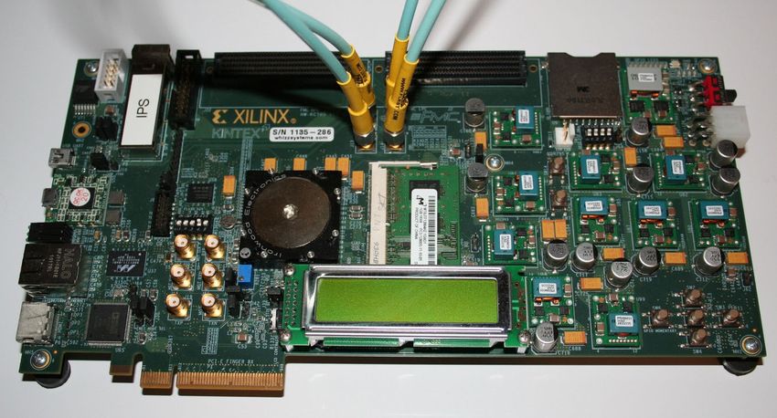
Running the Example Design on Hardware
The example design runs on a Kintex®-7 FPGA KC705 evaluation board and requires two pairs
of SMA cables to connect the GPIO SMA connectors, as shown in Figure 12.
X-Ref Target - Figure 12
;BB
Figure 12: Hardware Setup
Within the Vivado IDE, select Generate Bitstream within the flow navigator. This generates the
bitstream that targets the KC705 board. After the bitstream is generated, program the FPGA
within the Vivado hardware manager so that the integrated logic analyzer (ILA) core can be
used. The ILA core within the example project only works with Vivado hardware manager, not
iMPACT.
Within the hardware manager, run a Trigger Immediate to view the data transmitted and
received. The data transmitted should be equivalent to the received data. Figure 13 illustrates
the ILA data.
X-Ref Target - Figure 13
;BB
Figure 13: ILA Data
To purposely invoke an error, disconnect the SMA cables and the error LED lights up.
Reconnecting the cable and pulsing reset (GPIO_SW_S) turns the error LED (GPIO_LED_2_LS) off.
XAPP1217 (v1.0) March 17, 2015 www.xilinx.com 14Implementing the Reference Design
Running the Example Simulation
To run the example simulation, select Run Behavioral Simulation within the flow navigator of
the Vivado IDE, as shown in Figure 14. This launches a behavioral simulation with Vivado
simulator.
X-Ref Target - Figure 14
;BB
Figure 14: Running the Example Behavioral Simulation
The example simulation test bench connects the transmitter to the receiver and emulates jitter
with the assignment to the data_path_board_jitter signal. This allows the calibration state
machine to be stressed as it would be on a physical board. Be sure to run the simulation for at
least 400 µs to ensure that calibration completes.
The wave configuration file is set up to show the signals of the data checker module, as shown
in Figure 15.
X-Ref Target - Figure 15
;BB
Figure 15: Example Waveform after Running Behavioral Simulation
XAPP1217 (v1.0) March 17, 2015 www.xilinx.com 15How to Include the IP in a Custom Design
How to Include the IP in a Custom Design
The IP blocks provided in this application note are provided in the packaged_ip directory. To
include this IP into a custom design, the packaged IP needs to be included in the IP repository.
Go to the Project Settings and select the packaged_ip directory, as shown in Figure 16. Then
click OK.
X-Ref Target - Figure 16
;BB
Figure 16: Adding IP to Repository
After mapping the repository to the packaged IP, the I/O MUX IP appears in the IP catalog, as
shown in Figure 17.
X-Ref Target - Figure 17
;BB
Figure 17: Viewing the IP within the IP Catalog
XAPP1217 (v1.0) March 17, 2015 www.xilinx.com 16Resource Utilization
Resource Utilization
Table 5 and Table 6 provide a reference for the size of the transmitter and receiver with a
FULL_WIDTH parameter set to 32. The designs were intended to be as lightweight as possible.
Table 5: Transmitter Utilization
Data Width LUTs Flip-Flops
16 18 19
20 22 23
24 26 27
Table 6: Receiver Utilization
Valid Bits LUTs Flip-Flops
16 60 80
20 63 92
24 65 104
File Structure
Figure 18 shows the directory structure of the reference design:
X-Ref Target - Figure 18
[DSSLRPX[]LS
,3 FRQVWUDLQWV 3DFNDJHGBLS SURMHFW VLP UWOBVRXUFH
WRS[GF EXLOGBSURMHFWWFO WRSBWEY GDWDBFKHFNHUY
VWLPXOXVY
V\QFURY
WRSY
FORFNLQJBEORFN LRBPX[BLQB LRBPX[BRXWB LRBPX[BLQ LRBPX[BRXW
&ORFNLQJ:L]DUG,3 5HFHLYHU,3 7UDQVPLWWHU,3 5HFHLYHU 7UDQVPLWWHU
,QVWDQFH ,QVWDQFH ,QVWDQFH 3DFNDJHG,3 3DFNDJHG,3
;BB
Figure 18: Design File Hierarchy
XAPP1217 (v1.0) March 17, 2015 www.xilinx.com 17Table of Definitions
Table of Definitions
Table 7 defines some of the terms used in this application note.
Table 7: Table of Definitions
Term Definition
Valid bits The bits you are able to transmit and receive.
Potential valid bits The number of potential bits without relating the constraints at the user logic
boundaries.
Clipping bits The bits that are sent after the valid bits and are disregarded.
Parallel clock The user clock domain. This is generally a slow clock rate for emulation systems.
Serial clock The transmit and receive clock. This clock is faster than the parallel clock.
Effective MUX ratio This is the ratio of multiplexing to the user. The clipped bits are not included.
Actual MUX ratio This is the ratio between the parallel clock and the serial clock.
Conclusion
FPGAs are commonly used to emulate complex ASIC designs that span several of the largest
FPGAs. Sometimes, thousands of signals need to go between FPGAs. This application note
provides the ASIC designer a method of multiplexing I/Os without introducing any cycles of
latency.
Reference Design
You can download the Reference Design Files for this application note from the Xilinx website.
Table 8 shows the reference design matrix.
Table 8: Reference Design Matrix
Parameter Description
General
Developer name Luis Bielich
Target devices Kintex-7 FPGAs
Source code provided? Yes
Source code format (if provided) RTL, Tcl
Simulation
Functional simulation performed? Yes
Timing simulation performed? Yes
Test bench provided for functional and timing simulation? Both
XAPP1217 (v1.0) March 17, 2015 www.xilinx.com 18Revision History
Table 8: Reference Design Matrix (Cont’d)
Parameter Description
Test bench format Verilog/SystemVerilog
Simulator software and version Vivado simulator
SPICE/IBIS simulations N/A
Implementation software tool(s) and version 2014.4
Static timing analysis performed? Yes
Hardware Verification
Hardware verified? Yes
Platform used for verification KC705 board
Revision History
The following table shows the revision history for this document.
Date Version Revision
03/17/2015 1.0 Initial Xilinx release.
Please Read: Important Legal Notices
The information disclosed to you hereunder (the “Materials”) is provided solely for the selection and use of Xilinx products. To the
maximum extent permitted by applicable law: (1) Materials are made available "AS IS" and with all faults, Xilinx hereby DISCLAIMS ALL
WARRANTIES AND CONDITIONS, EXPRESS, IMPLIED, OR STATUTORY, INCLUDING BUT NOT LIMITED TO WARRANTIES OF
MERCHANTABILITY, NON-INFRINGEMENT, OR FITNESS FOR ANY PARTICULAR PURPOSE; and (2) Xilinx shall not be liable (whether in
contract or tort, including negligence, or under any other theory of liability) for any loss or damage of any kind or nature related to,
arising under, or in connection with, the Materials (including your use of the Materials), including for any direct, indirect, special,
incidental, or consequential loss or damage (including loss of data, profits, goodwill, or any type of loss or damage suffered as a result
of any action brought by a third party) even if such damage or loss was reasonably foreseeable or Xilinx had been advised of the
possibility of the same. Xilinx assumes no obligation to correct any errors contained in the Materials or to notify you of updates to the
Materials or to product specifications. You may not reproduce, modify, distribute, or publicly display the Materials without prior written
consent. Certain products are subject to the terms and conditions of Xilinx’s limited warranty, please refer to Xilinx’s Terms of Sale which
can be viewed at http://www.xilinx.com/legal.htm#tos; IP cores may be subject to warranty and support terms contained in a license
issued to you by Xilinx. Xilinx products are not designed or intended to be fail-safe or for use in any application requiring fail-safe
performance; you assume sole risk and liability for use of Xilinx products in such critical applications, please refer to Xilinx’s Terms of
Sale which can be viewed at http://www.xilinx.com/legal.htm#tos.
Automotive Applications Disclaimer
XILINX PRODUCTS ARE NOT DESIGNED OR INTENDED TO BE FAIL-SAFE, OR FOR USE IN ANY APPLICATION REQUIRING FAIL-SAFE
PERFORMANCE, SUCH AS APPLICATIONS RELATED TO: (I) THE DEPLOYMENT OF AIRBAGS, (II) CONTROL OF A VEHICLE, UNLESS THERE
IS A FAIL-SAFE OR REDUNDANCY FEATURE (WHICH DOES NOT INCLUDE USE OF SOFTWARE IN THE XILINX DEVICE TO IMPLEMENT THE
REDUNDANCY) AND A WARNING SIGNAL UPON FAILURE TO THE OPERATOR, OR (III) USES THAT COULD LEAD TO DEATH OR
PERSONAL INJURY. CUSTOMER ASSUMES THE SOLE RISK AND LIABILITY OF ANY USE OF XILINX PRODUCTS IN SUCH APPLICATIONS.
© Copyright 2015 Xilinx, Inc. Xilinx, the Xilinx logo, Artix, ISE, Kintex, Spartan, Virtex, Vivado, Zynq, and other designated brands
included herein are trademarks of Xilinx in the United States and other countries. All other trademarks are the property of their
respective owners.
XAPP1217 (v1.0) March 17, 2015 www.xilinx.com 19You can also read