168-195 GHZ POWER AMPLIFIER WITH OUTPUT POWER LARGER THAN 18 DBM IN BICMOS TECHNOLOGY
←
→
Page content transcription
If your browser does not render page correctly, please read the page content below
Received March 27, 2020, accepted April 19, 2020, date of publication April 27, 2020, date of current version May 12, 2020.
Digital Object Identifier 10.1109/ACCESS.2020.2990681

168-195 GHz Power Amplifier With Output
Power Larger Than 18 dBm in BiCMOS
Technology
ABDUL ALI 1,2 , JONGWON YUN 2,3 , FRANCO GIANNINI 1 ,
HERMAN JALLI NG 2,4 , (Member, IEEE), DIETMAR KISSINGER                                                  5,   (Senior Member, IEEE),
AND PAOLO COLANTONIO 1 , (Senior Member, IEEE)
1 Department    of Electronic Engineering, University of Rome Tor Vergata, 00133 Rome, Italy
2 IHP—Leibniz-Institut    für innovative Mikroelektronik, 15236 Frankfurt (Oder), Germany
3 Samsung    Electronics, Gyeonggi 18448, South Korea
4 Karlsruhe University of Applied Sciences, 76133 Karlsruhe, Germany
5 Institute of Electron Devices and Circuits, Ulm University, 89081 Ulm, Germany

Corresponding author: Abdul Ali (abdul.ali@uniroma2.it)
This work was supported by the H2020 ITN CELTA of Call: H2020-MSCA-ITN-2015 under Grant 675683.

  ABSTRACT This paper presents a 4-way combined G-band power amplifier (PA) fabricated with a
  130-nm SiGe BiCMOS process. First, a single-ended PA based on the cascode topology (CT) is designed
  at 185 GHz, which consists of three stages to get an overall gain and an output power higher than 27 dB
  and 13 dBm, respectively. Then, a 4-way combiner/splitter was designed using low-loss transmission lines
  at 130-210 GHz. Finally, the combiner was loaded with four single-ended PAs to complete the design of a
  4-way combined PA. The chip of the fabricated PA occupies an area of 1.35 mm2 . The realized PA shows a
  saturated output power of 18.1 dBm with a peak gain of 25.9 dB and power-added efficiency (PAE) of 3.5 %
  at 185 GHz. A maximum output power of 18.7 dBm with PAE of 4.4 % is achieved at 170 GHz. The 3-dB
  and 6-dB bandwidth of the PA are 27 and 42 GHz, respectively. In addition, the PA delivers a saturated output
  power higher than 18 dBm in the frequency range 140-186 GHz. To the best of our knowledge, the power
  reported in this paper is the highest for G-band SiGe BiCMOS PAs.

  INDEX TERMS Cascode, 4-way combiner, G-band PA, power amplifier, SiGe BiCMOS.

I. INTRODUCTION                                                                                short-range wireless communication, high-resolution imag-
With the recent progress in the speed of solid-state devices,                                  ing, sensing, phased arrays, and radar systems [7]–[15].
millimeter-waves and terahertz technologies are continuously                                      One of the key issues in the realization of high-frequency
improving in terms of cutoff frequency (fT ) and maximum                                       systems is the limited output power-level attainable with SiGe
oscillation frequency (fmax ). This includes transistors based                                 HBTs (heterojunction bipolar transistors). The low break-
on III-V (InP, GaAs) and Si (SiGe BiCMOS, CMOS) tech-                                          down voltage and scaling down of the transistor periphery to
nologies [1]–[6]. Generally, III-V (InP) transistors demon-                                    increase the fT and fmax leads to the limitation of obtaining
strate higher fT /fmax , and breakdown voltages (BVCEO and                                     high-output power. Additionally, dominant high-frequency
BVCBO ) compared to Si devices. Nevertheless, Si devices are                                   effects in terms of high conductor/substrate losses and
preferred over III-V devices due to their advantage in large-                                  increased parasitic elements of the transistor reduce its output
scale and high-level integration. Besides, advanced SiGe                                       power. These challenges make it difficult to design efficient
BiCMOS technologies exhibit fmax up to 500 GHz, which                                          and high power solid-state circuits such as voltage controlled
have allowed the development of solid-state systems above                                      oscillators (VCOs) [16], frequency multipliers [17], [18],
100 GHz for different applications including high-speed                                        and power amplifiers (PAs) [19], [20].
                                                                                                  To increase the output power (Pout ) and power added
                                                                                               efficiency (PAE), various high-frequency PAs based on
   The associate editor coordinating the review of this manuscript and                         SiGe BiCMOS technology have been reported in [19]–[25].
approving it for publication was Vittorio Camarchia              .                             They can be categorized into single-ended, N -way power

                     This work is licensed under a Creative Commons Attribution 4.0 License. For more information, see https://creativecommons.org/licenses/by/4.0/
VOLUME 8, 2020                                                                                                                                                        79299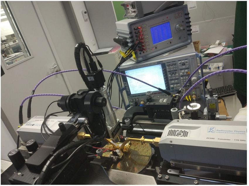
A. Ali et al.: 168-195 GHz PA With Output Power Larger Than 18 dBm in BiCMOS Technology

combined, and balanced (differential) PAs. These PAs are              splitter, four single-ended PAs, and an output combiner. For
designed using cascode topology (CT), common emitter (CE)             the first time, a G-band silicon PA exceeding an output
and stacked configurations. Single-ended PAs are usually              power of 18 dBm with a PAE larger than 3 % has been
compact and can be utilized in power combiner circuits to             demonstrated. This performance has been made possible by
obtain large output power. Examples of single-ended PAs are           exploiting the unique features of the 130-nm SiGe technology
reported in [19], [20] at various frequencies in the range of         from IHP with fT /fmax of 300/450 GHz and back-end-of-the-
110-140 GHz, which are based on CE and CT. Among them,                line (BEOL) process suited for millimeter wave applications.
a maximum output power of 13.8 dBm with PAE of 11.6 % is              The circuit can be used in frequency multiplier chains, radar
achieved at 116 GHz.                                                  sensors, and high-speed wireless communication transceivers
   The second most popular category to generate high output           operating in the 140-200 GHz band. The paper is organized as
power are N -way power combined PAs, which can be further             follows : In section II, the features of 130-nm SiGe BiCMOS
classified by the nature of combining networks into reactive,         technology are discussed. Section III presents the architecture
sub-quarter-wavelength balun, transformers, Wilkinson, and            of the 4-way combined PA. Then, section IV presents the
antenna-based free-space combiners [20]–[32]. For instance,           detailed design procedure for the single-ended PA, 4-way
the authors of [20], report an 8-way reactive power combined          combiner, and their integration for the realization of the
PA using CE configuration at 116 GHz. This PA despite                 overall PA. The experimental results and comparisons with
consuming a large amount of chip area delivers a maximum              state-of-the-art works are presented in section V. Finally, the
output power of 20.8 dBm with peak PAE and gain of 7.5 %,             conclusion and summary are reported in section VI.
and 15 dB, respectively. A PA solution with reduced area
consumption based on sub-quarter-wavelength baluns and                 II. 130-nm SiGe BiCMOS TECHNOLOGY
stacked configuration in [21] delivers a peak output power            The 4-way combined PA proposed in this paper was
of 22 dBm with PAE of 3.6 % at 120 GHz. However, the                  designed and fabricated with commercial IHP’s 130-nm SiGe
peak power gain of this PA is limited to 7.7 dB. Contrarily,          BiCMOS process known as SG13G2. The process offers
solutions based on transformers, Wilkinson combiners, and             high performance heterojunction bipolar transistors (HBTs)
free-space antenna combining networks [22]–[25], become               with fT /(fmax ) of 300/450 GHz and breakdown voltages of
unpractical for the design of high-frequency PAs. In fact,            BVCEO = 1.7 V, and BVCBO = 4.8 V, respectively [1].
the Wilkinson and transformer combiners introduce higher              The HBTs are highly suitable for the design of various mm-
losses when the number of combining networks increases,               wave and sub-THz circuits, which is further supported by the
while the free space losses and poor radiation efficiency of the      back-end-of-the-line (BEOL) process as shown in Fig. 1. The
high-frequency antennas limit the effective attainable output         BEOL provides seven metal layers based on aluminum(Al),
power.                                                                which include two thick low-loss metals (TM2 3 µm thick
   The third category of high-frequency PAs is based on dif-          and TM1 2 µm thick) and five thin metal layers (M5 -M1 each
ferential configurations, which benefits from the availability        0.49 µm thick). The top thick metals allow higher current
of virtual ground and presents high common-mode rejection             densities and present lower sheet resistance, while the lower
ratio (CMRR) for common-mode noise cancellation. Baluns               thin metals help to form various metal contact patterns for dif-
are required for differential to single-ended transformation,         ferent Si-devices. The metal layers together with their heights
which eases the characterization of the differential PAs.             and thickness enable the customized realization of high-
Examples of differential PAs without utilizing power com-             quality inductors, metal-oxide-metal (MOM) capacitors, and
bining networks are reported in [26]–[29], where a maxi-              transmission lines such as microstrip and coplanar lines. The
mum output power of 14 dBm with a peak gain of 27 dB is               lower metal layers permit the design of ground plane and
demonstrated at 160 GHz. The designs of 4-way combined                dense metal interconnections. In addition, the process offers
differential PAs at 170 and 240 GHz using T-junctions are
discussed in [30], [31]. A maximum output power of 18 dBm
is achieved at 170 GHz by de-embedding the loss of RF pads
and baluns. However, this PA is partially characterized, while
a full characterization to see the large-signal performance
across all frequency bands should be shown. There are very
few examples of the high-frequency PAs around 160 GHz in
SiGe BiCMOS technology and most of the reported designs
demonstrate high-output power in the lower D-band. G-band
PAs above 160 GHz with large output power are crucial to
drive frequency multipliers for the generation of high-power
sub-THz signals.
   In this paper, we report a G-band (168-195 GHz) 4-way
combined solid-state PA based on 130-nm SiGe BiCMOS
technology [32]. The complete G-band PA includes an input             FIGURE 1. BEOL Cross-section of 130-nm SiGe BiCMOS technology [33].

79300                                                                                                                             VOLUME 8, 2020
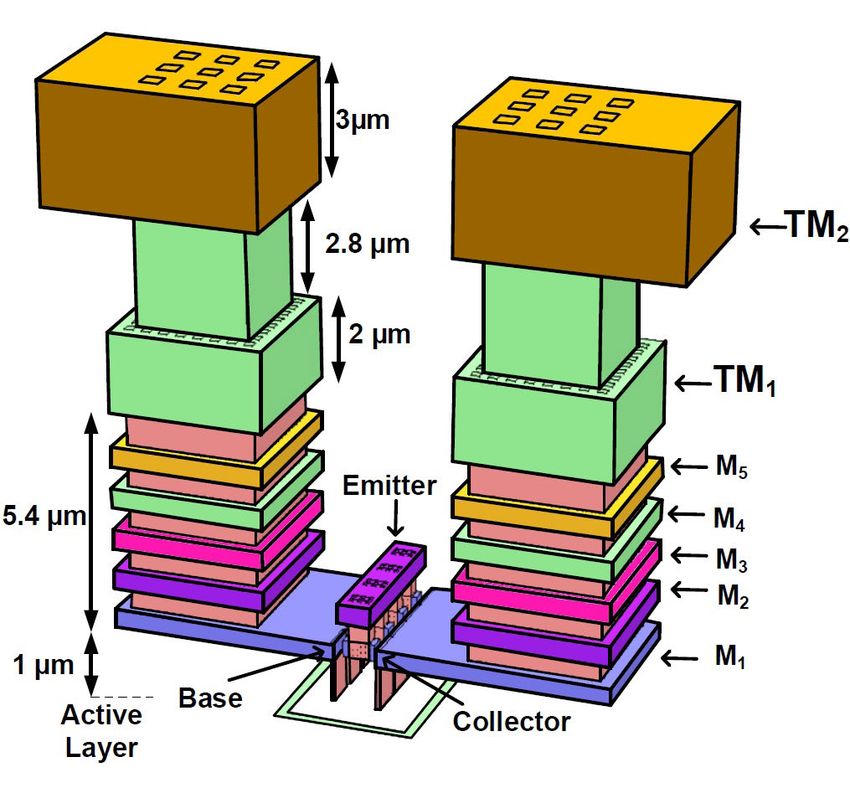
A. Ali et al.: 168-195 GHz PA With Output Power Larger Than 18 dBm in BiCMOS Technology

polysilicon resistors and high quality-factor metal-insulator-
metal (MIM) capacitors.

III. ARCHITECTURE OF THE 4-WAY COMBINED PA
Fig. 2 shows the block diagram of the G-band 4-way com-
bined PA. It consists of an input splitter, four-unit cells of
single-ended PAs, and an output combiner. The proposed
structure was aimed to provide a peak output power of more
than 18 dBm with a power gain larger than 27 dB at 185 GHz.
Assuming ideal lossless components in the design, a unit cell                  FIGURE 3. Schematic of CE (a) and CT (b).
PA (single-ended PA) is able to provide an output power more
than 12 dBm with a power gain of 27 dB, which leads to an
output power of 18 dBm in a 4-way combination. However,                        of 2.0 mA/µm. Biasing resistors R1−2 with values in the
in the actual case with lossy components, the unit cell should                 range 300-500  were added at the bases of each transistor
provide an output power well above 12 dBm to compensate                        for optimal gain and output power, which allows the effective
the loss of power combiner.                                                    collector-emitter breakdown voltage to increase well above
                                                                               BVCEO by presenting an external low impedance to the bases
                                                                               of the transistors [20], [34]. Fig. 4 shows the maximum avail-
                                                                               able gain (MAG) and stability factor (µ1 ) for the CE and CT
                                                                               without including the physical metal interconnections. It is
                                                                               noted that the CT shows higher gain and stability compared
                                                                               to the CE. Specifically, at 185 GHz, the CT and CE show a
                                                                               MAG of 12.3 dB and 6.3 dB, respectively. Moreover, better
                                                                               isolation between the input and output of the CT ensures
                                                                               higher stability with respect to the CE.

FIGURE 2. Block diagram of the G-band 4-way combined PA.

   Assuming the input and output of a unit cell is matched
to 50 , the splitting/combining networks must be designed
to ensure conjugate matching of the input and output of the
4-way combined PA and external 50  standard terminations.
Such transformation is ensured with the following steps:
the transmission lines TL1,2 were used to properly compen-                     FIGURE 4. Simulated MAG and µ1 -factor of the CE and CT.
sate the overall parasitic effects while roughly maintaining
50  on the up and down side of section A (i.e., at A the                         For the design of high-frequency power amplifiers, it is
impedance seen is roughly 25 ) then, through the trans-                       certainly more interesting to compare the large-signal per-
mission lines TL3,4 the impedance is transformed to 50 .                      formance of the two topologies. Load-pull simulations were
This will again make the impedance seen at the junction of                     performed to find the optimum load impedances resulting in
node B 25 , which is finally transformed to 50  at node C                    maximum output power and PAE at 185 GHz, while the input
using TL5,6 and parasitic capacitance of the RF pad.                           was terminated on the conjugate matching condition. Table 1
                                                                               shows the relevant parameters (input and load impedances,
IV. CIRCUIT DESIGN CONSIDERATIONS
A. PA TOPOLOGY
The design of the high-frequency PA requires the investiga-                    TABLE 1. Performance parameters of CE and CT at 185 GHz.

tion of various topologies in terms of gain, output power, and
power added efficiency (PAE). CE and CT are the two most
adopted solutions for the design of high-frequency PAs. The
schematics of a CE and a CT are shown in Fig. 3(a) and 3(b),
respectively.
   To compare the two topologies, the transistors shown
in Fig. 3 are biased at a collector current density

VOLUME 8, 2020                                                                                                                            79301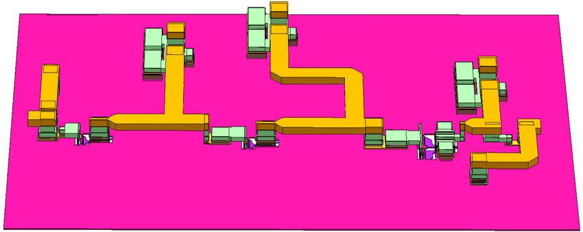
A. Ali et al.: 168-195 GHz PA With Output Power Larger Than 18 dBm in BiCMOS Technology

                                                                            FIGURE 6. fT and fmax of the transistor versus collector current density
FIGURE 5. Simulated gain, output power, and PAE of CE and CT                without (W/O) and with (W) parasitic extracted.
at 185 GHz.
                                                                            TABLE 2. Performance parameters of CT without (W/O) and with (W)
                                                                            interconnects at 185 GHz.

peak gain, output power at 1 dB compression and at satura-
tion, and peak PAE) of CE and CT, while Fig. 5 illustrates
the power sweep curves resulting from nonlinear harmonic
balance simulations under optimum load/source terminations
at 185 GHz. It is noted that the two topologies show almost
similar input impedance. The CT shows larger optimum
load resistance (RLopt,CT = 87 ) with respect to CE
(RLopt,CE = 22.42 ). In terms of output power and gain,
the CT shows higher values than CE. Both CE and CT show
almost similar PAE of about 20 %. However, when the inher-
ent losses introduced by the interconnections and matching
networks are taken into account at 185 GHz, it will result
in a severe reduction of the attainable gain, output power
and PAE. The lower gain resulting from the CE makes such
solution less attractive in comparison to the CT, which was
adopted for the design of the single-ended PA at 185 GHz.

B. UNIT CELL: SINGLE-ENDED PA
The high-frequency PA typically consists of a power stage
and finite driver stages. The former provides the required                  FIGURE 7. Simulated gain, output power, and PAE of the CT power-stage
                                                                            without (W/O) and with (W) interconnections at 185 GHz.
output power, whereas the latter allows to satisfy the gain
specification. To design a power stage with output power
higher than 13 dBm at 185 GHz, the active area of each                         It is noted that the interconnections introduce a loss
transistor in CT was picked as an aggregation of two parallel               of 1.6 dB, which reduces the peak gain from 12.2 to 10.6 dB.
8-finger HBTs (see Fig.3(b)). This provides a saturated output              The output power, PAE, and optimum input/load impedances
power of 15.8 dBm without including metallic interconnec-                   are also affected by the interconnections. The maximum
tions. Suitable metal interconnections were designed for the                power and PAE are dropped to 14.7 dBm, and 14.6 %, respec-
power stage to satisfy metal current density and electro-                   tively, due to the loss introduced by the interconnections.
migration rules. The interconnections were EM-simulated in                     To drive the power stage and attain an overall gain larger
ADS-Momentum from Keysight to see their effect on fT /fmax ,                than 27 dB, two identical driver stages were adopted. The
output power, gain and PAE. Fig. 6 shows the fT /fmax of the                transistor’s size in the driver stages is half with respect
transistor with parasitics extracted (with interconnects). The              to power stage. Table 3 provides summary of the different
fT /fmax drops from 300/450 GHz to 270/350 GHz, which                       parameters of the two driver stages biased with voltage sup-
is still better than CMOS [35]. This degradation in fT /fmax                plies of 3 V and 4 V for the 1st and 2nd stage, respectively.
reduces the output power, gain and PAE of the PA.                           4 V supply could be selected for the 1st driver stage instead
    Load-pull simulations were repeated to optimize output                  of 3 V to increase the overall gain. However, 3 V supply was
power, and PAE at 185 GHz. The resulting parameters of the                  opted to reduce the total DC power consumption of the PA.
power stage without (lossless, i.e., ideal) and with intercon-                 The optimum impedances required by each stage were
nections are summarized in Table 2, while Fig. 7 shows the                  properly synthesized through the design of the input, inter-
output power, gain and PAE curves at 185 GHz.                               stages, and output matching networks to complete the

79302                                                                                                                                   VOLUME 8, 2020
A. Ali et al.: 168-195 GHz PA With Output Power Larger Than 18 dBm in BiCMOS Technology
FIGURE 8. Schematic of the: a) single-ended PA and its b) 3D layout view.
TABLE 3. Performance parameters of driver stages with interconnects
at 185 GHz.
design of the single-ended PA. The matching networks were
designed using MIM capacitors, and 50 transmission lines
with different electrical lengths. The DC-block capacitors
were optimized as part of the matching networks. Unlike high
impedance lines, 50 transmission lines have been utilized
for sustaining higher current densities, which improves the FIGURE 9. Simulated S-parameters of the single-ended PA.
reliability of the PA. The three stages of the single-ended PA
were AC coupled by using bypass capacitors. The matching
networks, including bypass capacitors were EM-simulated in summation of the gains of each stage due to the loss of
ADS momentum. Fig. 8(a) shows the final schematic of the matching networks. Fig. 10 shows the gain, output power, and
single-ended PA, while the corresponding 3D-layout is shown PAE of the single-ended PA at 185 GHz. A peak output power
in Fig. 8(b). of 13.1 dBm with a PAE of 7.7 % is obtained. To quantify
Fig. 9 shows the simulated S-parameters of the single- the losses associated with the matching networks, Fig. 11 was
ended PA. A good matching is achieved at the input generated where the output power is reported at various nodes
(|S11 | < −10 dB) and output (|S22 | < −10 dB) with a gain of (see Fig. 8(a)). For the ease of readability, the powers are
28.2 dB at 185 GHz, which is inherently smaller than the also specified for a fixed input power of −18 dBm in the
VOLUME 8, 2020 79303A. Ali et al.: 168-195 GHz PA With Output Power Larger Than 18 dBm in BiCMOS Technology
combiner/splitter illustrating various transmission lines with
different characteristic impedances and electrical lengths.
The combiner was optimized in ADS-momentum, while
ensuring good matching at each nodes (see points A, B, and C
in Fig. 2).
Fig. 13 shows the simulated S-parameters of the 4-way
combiner. A good matching is achieved in wide bandwidth
with both |S11 | and |S22 | better than −10 dB at 130-270 GHz.
The combiner presents an insertion loss less than 1 dB
at 140-205 GHz.
FIGURE 10. Simulated gain, output power, and PAE of the single-ended
PA at 185 GHz.
FIGURE 13. Simulated S-parameters of the 4-way combiner/splitter.
D. 4-WAY COMBINED PA IMPLEMENTATION
The transmission lines used in the matching networks and
power combiner were realized using top thick metal (TM2 )
FIGURE 11. Simulated output power at various nodes of the single-ended for the RF lines with bottom thin metal M3 acting as the
PA at 185 GHz. ground plane (See Fig. 1). The lower metals M1 and M2 were
used for various interconnections to route DC lines. Separate
same figure. The input, first interstage, second interstage, collector and base supplies were used to bias the transistor.
and output matching networks introduced loss of 1.4, 1.15, Besides, collector supplies of each stage are separated to
1.41, and 1.16 dB, respectively. The overall loss of the passive improve stability. Additionally, Large bypass capacitors with
networks is 5.12 dB. a series resistor of 10 are included in the supply lines.
The full layout of the 4-way combined PA consists of
C. 4-WAY SPLITTER/COMBINER integrated input splitter, four-unit cells of single-ended PAs,
To combine the four-unit cells of single-ended PAs, a low- output combiner and bonding pads. The final PA was fabri-
loss 4-way splitter/combiner earlier discussed in section III cated with the standard 130-nm SiGe BiCMOS process and
was designed. Fig. 12 shows the final layout of the 4-way its micro-photograph is shown in Fig. 14. It occupies a very
small area of 0.97 × 1.4 mm2 , including RF and DC pads.
It is noted that the chip contains dummy metal layers, which
were included to satisfy the metal density rules of the 130-nm
BEOL process. Such dummy metal layers were placed at least
30-50 µm away from the RF lines to avoid any coupling with
the main circuitry, which was further verified by including
them in EM-simulation during the design of the matching
networks.
V. EXPERIMENTAL RESULTS
The realized power amplifier was characterized on wafer
under small and large signal conditions. During the char-
acterization, the supply voltages were set as VCC1 = 3 V,
FIGURE 12. Layout of the 4-way combiner/splitter. VCC2 = 4.0 V, and VCC3 = 4.0 V.
79304 VOLUME 8, 2020A. Ali et al.: 168-195 GHz PA With Output Power Larger Than 18 dBm in BiCMOS Technology
FIGURE 14. Chip micro-photograph of the 4-way combined PA
(0.97 × 1.4 mm2 including pads).
FIGURE 15. S-parameters measurement setup showing different blocks
in WR-4.0 band.
FIGURE 17. (a) Stability factor (µ1 ) and (b) S-parameters of the 4-way
combined PA. The stability factor is compared to the single-ended PA.
FIGURE 16. In-house measurement setup at IHP for the characterization
of S-parameters of the 4-way combined PA in G-band.
FIGURE 18. Output power measurement setup in D-band using ZC170
frequency extender.
A. SMALL-SIGNAL
The small-signal (S-parameters) characterization was carried
out using the setup shown in Fig. 15. The Rohde & Schwarz in G-band. The input RF (RFin ) and LO (LOin ) signals of
ZVA67 VNA (Vector Network Analyzer) and ZC260 fre- the frequency extender are generated by the VNA and locked
quency extender were used to perform measurements with the frequency of measurement, i.e., RFin = RF/12
VOLUME 8, 2020 79305A. Ali et al.: 168-195 GHz PA With Output Power Larger Than 18 dBm in BiCMOS Technology
FIGURE 19. Experimental output power, gain, and PAE of the 4-way combined PA: (a) at 160 GHz, (b) at 170 GHz, and (c) at 185 GHz.
and LOin = (RF − 279MHz)/12. The LOin signal is further
divided into two using a power divider. These RFin and LOin
signals then feed the two ZC260 frequency extenders, which
generates the required RFout signals needed to feed the two
terminal device under test (DUT i.e., PA in this case). The
DUT contains an identical set of DC and RF probes, and
waveguide fixtures at each side. The reflected and measured
intermediate frequency (IF) signals (279 MHz) are later cap-
tured by the VNA. The multiplication factors for the ZVA260
frequency extenders are 12. In addition, the attenuator of the
frequency extender can be used to adjust the incident power
of the RF signal feeding the DUT.
Similar setup with the replacement of RF probe and
frequency extender (ZC170) was used to measure the FIGURE 20. Measured and simulated output power of the 4-way
S-parameters of the PA in D-band (110-170 GHz). A photo of combined PA at 3-dB back-off and saturation.
the measurement setup available at IHP laboratory is shown
in Fig. 16.
Fig 17(a) and Fig 17(b) show the stability-factor (µ1 ) and
measurement setup. The input signal feeds the DUT, which
S-parameters of the 4-way combined PA, respectively. In gen-
is generated using similar method discussed in section V-A.
eral a good co-relation is found between the simulation and
The amplified signal at the output of DUT is detected by the
measurement. The PA is stable as the µ1 -factor is above 1.
VDI Erickson PM5 power meter. For the characterization in
The measured stability is only shown at 110-260 GHz due to
G-band, the frequency extender ZC170 was replaced with
non-availability of RF probes and sources to cover a large
ZC260, while WR 4.0 probes were adopted. The loss of
frequency range from DC to fmax . Nevertheless, the simulated
RF-probes found from the data-sheet was de-embedded in the
stability of the PA was assessed under even and odd-mode
power measurement.
excitation and it was found unconditionally stable. Also,
Fig. 19 shows the measured large-signal parameters of the
the single-ended and 4-way combined PAs are uncondition-
4-way combined PA compared with the simulation. These
ally stable. The PA shows a maximum small-signal gain of
parameters include output power, gain, and PAE at var-
25.9 dB with |S11 | and |S22 | better than −10 dB at 185 GHz.
ious frequencies in G-band. The PA shows almost simi-
The measured gain at 185 GHz is slightly (1.3 dB) lower than
lar performance in terms of maximum output power with
the simulated one (27.2 dB). The discontinuity at 170 GHz is
the difference in gain. For instance, at 185 GHz, the PA
clearly related to the change of measurement set-up (D- or
achieves 18.1 dBm of saturated output power with 25.9 dB
G-band). The 3 dB and 6 dB bandwidth of the PA are 27 GHz
of peak gain and 3.5 % of PAE. Similarly, a maximum out-
and 42 GHz, respectively.
put power of 18.7 dBm with a PAE of 4.4 % is demon-
strated at 170 GHz. The degradation in measured PAE is
B. LARGE-SIGNAL due to the output power and gain, which are lower than
The large-signal characterization of the PA was performed the simulation. Nevertheless, a good correlation is found
using a setup similar to the small-signal test bench with between them. The PA consumed maximum overall dc
the difference in the use of a power meter at the out- current of 431 mA, which is the sum of currents from
put of the DUT. Fig. 18 shows the D-band output power each supply (VCC1 = 3 V, ICC1 = 85.4 mA, VCC2 = 4 V,
79306 VOLUME 8, 2020A. Ali et al.: 168-195 GHz PA With Output Power Larger Than 18 dBm in BiCMOS Technology
TABLE 4. State of the Art PAs comparison. Parameters of the PAs are shown at the frequency, which resulted in maximum output power.
ICC2 = 102.7 mA, VCC2 = 4 V, ICC2 = 242.9 mA). consumption of the PA without significantly degrading the
The resulting overall dc power consumption is about 1.6 W. large-signal performance. The procedure adopted in this
Fig. 20 shows the simulated and measured output power paper can be applied at higher frequencies above 200 GHz
at 3-dB back-off and at saturation. In the simulation, the to design high power PA. Also, the PA can be utilized in
saturated output power is found for a fixed input of 5 dBm. the design of different solid-state systems for various future
The PA provides a 3-dB back-off output power larger applications.
than 15 dBm and a Psat larger than 18 dBm at frequencies
≈140-186 GHz. Such performances make the PA highly ACKNOWLEDGMENT
desirable for various broadband applications. The authors would like to thank IHP for providing chip area
Table 4 shows summary of the various parameters of state- for the fabrication of PA. They would also like to thank
of-the-art PAs based on both Si (SiGe BiCMOS, CMOS) J. Borngräber for his assistance in the measurement.
and III-V (InP, GaAs) technologies at various frequencies in
D and G-bands. Advanced InP process achieves high output REFERENCES
power and PAE than GaAs and Si based technologies. How- [1] B. Heinemann et al., ‘‘SiGe HBT technology with fT /fmax of
ever, SiGe BiCMOS is still getting close to InP with highest 300 GHz/500 GHz and 2.0 ps CML gate delay,’’ in IEDM Tech.
Dig., Dec. 2010, pp. 30.5.1–30.5.4.
power demonstrated in the lower D-band around 115 GHz. [2] D. Simic and P. Reynaert, ‘‘A 14.8 dBm 20.3 dB power amplifier for
Few works have shown high output power in the upper D-band applications in 40 nm CMOS,’’ in Proc. IEEE Radio Freq. Integr.
D-band, which are still not fully characterized. The PA pre- Circuits Symp. (RFIC), Jun. 2018, pp. 232–235.
[3] S. Diebold, P. Pahl, B. Goettel, H. Massler, A. Tessmann, A. Leuther,
sented in this work delivers high output power in the G-band T. Zwick, and I. Kallfass, ‘‘A 130 to 160 GHz broadband power amplifier
at f ≥ 170 GHz. Also, it achieved saturated output power with binary power splitting topology,’’ in Proc. Asia–Pacific Microw. Conf.,
≥ 18 dBm over a wide range of frequencies at 140-186 GHz, Dec. 2012, pp. 442–444.
[4] B. Amado-Rey, Y. Campos-Roca, C. Friesicke, F. van Raay, H. Massler,
which is state-of-the-art for SiGe BiCMOS technology. A. Leuther, and O. Ambacher, ‘‘A G -band broadband balanced power
amplifier module based on cascode mHEMTs,’’ IEEE Microw. Wireless
VI. CONCLUSION Compon. Lett., vol. 28, no. 10, pp. 924–926, Oct. 2018.
[5] Z. Griffith, M. Urteaga, and P. Rowell, ‘‘A 140-GHz 0.25-W PA and a 55-
A fully integrated G-band PA based on the 130-nm SiGe 135 GHz 115-135 mW PA, high-gain, broadband power amplifier MMICs
BiCMOS technology with an output power larger than in 250-nm InP HBT,’’ in IEEE MTT-S Int. Microw. Symp. Dig., Jun. 2019,
18 dBm is presented. The large-signal performance of the PA pp. 1245–1248.
[6] Z. Griffith, M. Urteaga, and P. Rowell, ‘‘A 115-185 GHz 75-115 mW high-
relies on the low-loss wide-band on-chip power combiner and gain PA MMIC in 250-nm InP HBT,’’ in Proc. 14th Eur. Microw. Integr.
single-ended PAs. Besides, detail procedure about the design Circuits Conf. (EuMIC), Sep. 2019, pp. 860–863.
of 4-way combined PA is presented, which includes selection [7] M. H. Eissa, A. Malignaggi, R. Wang, M. Elkhouly, K. Schmalz,
A. C. Ulusoy, and D. Kissinger, ‘‘Wideband 240-GHz transmitter and
of the topology, effect of the interconnections, schematic receiver in BiCMOS technology with 25-Gbit/s data rate,’’ IEEE J. Solid-
and complete layout of the single-ended PA, and four-way State Circuits, vol. 53, no. 9, pp. 2532–2542, Sep. 2018.
combiner. [8] Y. Zhao, E. Ojefors, K. Aufinger, T. F. Meister, and U. R. Pfeiffer,
‘‘A 160-GHz subharmonic transmitter and receiver chipset in an SiGe
The future work can focus on improving the small- HBT technology,’’ IEEE Trans. Microw. Theory Techn., vol. 60, no. 10,
signal bandwidth, reducing the DC power and chip area pp. 3286–3299, Oct. 2012.
VOLUME 8, 2020 79307A. Ali et al.: 168-195 GHz PA With Output Power Larger Than 18 dBm in BiCMOS Technology
[9] J. Grzyb, B. Heinemann, and U. R. Pfeiffer, ‘‘Solid-state terahertz super- [29] M. Furqan, F. Ahmed, B. Heinemann, and A. Stelzer, ‘‘A 15.5-dBm
resolution imaging device in 130-nm SiGe BiCMOS technology,’’ IEEE 160-GHz high-gain power amplifier in SiGe BiCMOS technology,’’ IEEE
Trans. Microw. Theory Techn., vol. 65, no. 11, pp. 4357–4372, Nov. 2017. Microw. Wireless Compon. Lett., vol. 27, no. 2, pp. 177–179, Feb. 2017.
[10] M. Uzunkol, O. D. Gurbuz, F. Golcuk, and G. M. Rebeiz, ‘‘A 0.32 THz [30] M. Kucharski, H. J. Ng, and D. Kissinger, ‘‘An 18 dBm 155-180 GHz SiGe
SiGe 4×4 imaging array using high-efficiency on-chip antennas,’’ IEEE J. power amplifier using a 4-Way T-junction combining network,’’ in Proc.
Solid-State Circuits, vol. 48, no. 9, pp. 2056–2066, Sep. 2013. IEEE 45th Eur. Solid State Circuits Conf. (ESSCIRC), Sep. 2019, pp. 1–4.
[11] I. Sarkas, J. Hasch, A. Balteanu, and S. P. Voinigescu, ‘‘A fundamen- [31] M. H. Eissa and D. Kissinger, ‘‘A 13.5 dBm fully integrated 200-to-
tal frequency 120-GHz SiGe BiCMOS distance sensor with integrated 255 GHz power amplifier with a 4-Way power combiner in SiGe:C
antenna,’’ IEEE Trans. Microw. Theory Techn., vol. 60, no. 3, pp. 795–812, BiCMOS,’’ in IEEE Int. Solid-State Circuits Conf. (ISSCC) Dig.
Mar. 2012. Tech. Papers, San Francisco, CA, USA, Feb. 2019, pp. 82–84, doi:
[12] W. Shin, O. Inac, Y.-C. Ou, B. Ku, and G. M. Rebeiz, ‘‘A -112 GHz- wafer- 10.1109/ISSCC.2019.8662424.
scale phased array transmitter with high-efficiency on-chip antennas,’’ in [32] A. Ali, P. Colantonio, F. Giannini, D. Kissinger, H. J. Ng, and J. Yun,
Proc. IEEE Radio Freq. Integr. Circuits Symp., Jun. 2012, pp. 199–202. ‘‘A 18-dBm G-band power amplifier using 130-nm SiGe BiCMOS technol-
ogy,’’ in Proc. 14th Eur. Microw. Integr. Circuits Conf. (EuMIC), Sep. 2019,
[13] B. Laemmle, K. Schmalz, J. C. Scheytt, R. Weigel, and D. Kissinger,
pp. 164–167.
‘‘A 125-GHz permittivity sensor with read-out circuit in a 250-nm SiGe
[33] A. Ali, J. Yun, H. Jalli Ng, D. Kissinger, F. Giannini, and P. Colan-
BiCMOS technology,’’ IEEE Trans. Microw. Theory Techn., vol. 61, no. 5,
tonio, ‘‘High performance asymmetric coupled line balun at sub-THz
pp. 2185–2194, May 2013.
frequency,’’ Appl. Sci., vol. 9, no. 9, p. 1907, 2019. [Online]. Available:
[14] J. Grzyb, K. Statnikov, N. Sarmah, B. Heinemann, and U. R. Pfeiffer, http://www.mdpi.com/2076-3417/9/9/1907
‘‘A 210–270-GHz circularly polarized FMCW radar with a single-lens- [34] M. Rickelt, H.-M. Rein, and E. Rose, ‘‘Influence of impact-ionization-
coupled SiGe HBT chip,’’ IEEE Trans. THz Sci. Technol., vol. 6, no. 6, induced instabilities on the maximum usable output voltage of Si-bipolar
pp. 771–783, Nov. 2016. transistors,’’ IEEE Trans. Electron Devices, vol. 48, no. 4, pp. 774–783,
[15] A. Mostajeran, A. Cathelin, and E. Afshari, ‘‘A 170-GHz fully integrated Apr. 2001.
single-chip FMCW imaging radar with 3-D imaging capability,’’ IEEE J. [35] O. Inac, M. Uzunkol, and G. M. Rebeiz, ‘‘45-nm CMOS SOI technology
Solid-State Circuits, vol. 52, no. 10, pp. 2721–2734, Oct. 2017. characterization for millimeter-wave applications,’’ IEEE Trans. Microw.
[16] R. Kananizadeh and O. Momeni, ‘‘A 190-GHz VCO with 20.7% tuning Theory Techn., vol. 62, no. 6, pp. 1301–1311, Jun. 2014.
range employing an active mode switching block in a 130 nm SiGe
BiCMOS,’’ IEEE J. Solid-State Circuits, vol. 52, no. 8, pp. 2094–2104,
Aug. 2017.
[17] H.-C. Lin and G. M. Rebeiz, ‘‘A SiGe multiplier array with output power of
5–8 dBm at 200–230 GHz,’’ IEEE Trans. Microw. Theory Techn., vol. 64,
ABDUL ALI was born in Quetta, Pakistan.
no. 7, pp. 2050–2058, Jul. 2016. He received the B.S. degree in telecommunication
[18] M. Kucharski, M. H. Eissa, A. Malignaggi, D. Wang, H. J. Ng, and
engineering from the National University of Com-
D. Kissinger, ‘‘D-band frequency quadruplers in BiCMOS technology,’’ puter and Emerging Sciences, Peshawar, Pakistan,
IEEE J. Solid-State Circuits, vol. 53, no. 9, pp. 2465–2478, Sep. 2018. in 2011, the M.S. degree in electrical and electron-
[19] D. Hou, Y.-Z. Xiong, W.-L. Goh, W. Hong, and M. Madihian, ‘‘A D-band ics engineering from Bilkent University, Ankara,
cascode amplifier with 24.3 dB gain and 7.7 dBm output power in 0.13 Turkey, in 2015, and the Ph.D. degree (Hons.)
µm SiGe BiCMOS technology,’’ IEEE Microw. Wireless Compon. Lett., in electronic engineering from the University of
vol. 22, no. 4, pp. 191–193, Apr. 2012. Rome Tor Vergata, Rome, Italy, in 2019.
[20] H.-C. Lin and G. M. Rebeiz, ‘‘A 110–134-GHz SiGe amplifier with peak Since, 2017, he has been with the Circuit Design
output power of 100-120 mW,’’ IEEE Trans. Microw. Theory Techn., Department, Innovations for High Performance Microelectronics (IHP),
vol. 62, no. 12, pp. 2990–3000, Dec. 2014. Frankfurt (Oder), Germany, where he is currently working as the Guest
[21] S. Daneshgar and J. F. Buckwalter, ‘‘A 22 dBm, 0.6 mm2 D-band Scientist for the design of circuits in the sub-THz frequency band. His current
SiGe HBT power amplifier using series power combining sub-quarter- research interests include millimeter-wave and sub-THz power amplifiers,
wavelength baluns,’’ in Proc. IEEE Compound Semiconductor Integr. Cir- frequency multipliers, and on-chip antennas for various applications.
cuit Symp. (CSICS), Oct. 2015, pp. 1–4. Dr. Ali was a recipient of the Gallium Arsenide (Gaas) Award, in 2019.
[22] Y. Zhao and J. R. Long, ‘‘A wideband, dual-path, millimeter-wave power
amplifier with 20 dBm output power and PAE above 15% in 130 nm SiGe-
BiCMOS,’’ IEEE J. Solid-State Circuits, vol. 47, no. 9, pp. 1981–1997,
Sep. 2012. JONGWON YUN received the B.S. and Ph.D.
[23] W. Tai, L. R. Carley, and D. S. Ricketts, ‘‘A 0.7 W fully integrated 42 GHz degrees from the School of Electrical Engineering,
power amplifier with 10% PAE in 0.13 µm SiGe BiCMOS,’’ in IEEE Korea University, Seoul, South Korea, in 2007 and
Int. Solid-State Circuits Conf. (ISSCC) Dig. Tech. Papers, Feb. 2013, 2015, respectively.
pp. 142–143. In 2015, he was a Research Professor with
[24] Y. A. Atesal, B. Cetinoneri, M. Chang, R. Alhalabi, and G. M. Rebeiz, the School of Electrical Engineering, Korea Uni-
‘‘Millimeter-wave wafer-scale silicon BiCMOS power amplifiers using
versity, where he focused on millimeter-wave
free-space power combining,’’ IEEE Trans. Microw. Theory Techn., vol. 59,
and THz circuits for imaging and communication
no. 4, pp. 954–965, Apr. 2011.
systems. From 2016 to 2017, he was with the
[25] A. Ali, J. Yun, H. J. Ng, D. Kissinger, F. Giannini, and P. Colantonio, ‘‘Sub-
Research and Development Division, SK Hynix,
THz on-chip dielectric resonator antenna with wideband performance,’’
in Proc. 14th Eur. Microw. Integr. Circuits Conf. (EuMIC), Sep. 2019,
Icheon, Gyeonggi, South Korea, as a Senior Research Engineer. From 2017
pp. 912–915. to 2019, he was a Scientist with the Circuit Design Department, Innovations
[26] J. Al-Eryani, H. Knapp, J. Wursthorn, K. Aufinger, S. Majied, H. Li, for High Performance Microelectronics (IHP), Frankfurt (Oder), Germany,
S. Boguth, R. Lachner, J. Bock, and L. Maurer, ‘‘A 162 GHz power where his research was focused on THz circuits and systems. Since 2019,
amplifier with 14 dBm output power,’’ in Proc. IEEE Bipolar/BiCMOS he has been with the Device Solution (DS) Division, Samsung Electronics,
Circuits Technol. Meeting (BCTM), Sep. 2016, pp. 174–177. Hwaseong, Gyeonggi, South Korea, as a Staff Engineer, where he is currently
[27] M. Kucharski, J. Borngraber, D. Wang, D. Kissinger, and H. J. Ng, ‘‘A responsible for the design and development of millimeter-wave circuits
109–137 GHz power amplifier in SiGe BiCMOS with 16.5 dBm out- for wireless applications. His research interests include high-frequency and
put power and 12.8% PAE,’’ in Proc. 47th Eur. Microw. Conf. (EuMC), high-speed integrated circuits and systems for sensing, imaging, and com-
Oct. 2017, pp. 1021–1024. munication applications.
[28] N. Sarmah, B. Heinemann, and U. R. Pfeiffer, ‘‘A 135–170 GHz power Dr. Yun was a co-recipient of the Best Student Paper Award of the IEEE
amplifier in an advanced sige HBT technology,’’ in Proc. IEEE Radio Freq. Radio Frequency Integration Technology Symposium, in 2015, and the
Integr. Circuits Symp. (RFIC), Jun. 2013, pp. 287–290. Gallium Arsenide (Gaas) Award, in 2019.
79308 VOLUME 8, 2020A. Ali et al.: 168-195 GHz PA With Output Power Larger Than 18 dBm in BiCMOS Technology
FRANCO GIANNINI was born in Galatina (LE), DIETMAR KISSINGER (Senior Member, IEEE)
Italy, in November 1944. He received the degree received the Dipl.-Ing., Dr.-Ing. and Habilita-
(summa cum laude) in electronics engineering tion degrees in electrical engineering from FAU
from the Warsaw University of Technology, Erlangen-Nürnberg, Germany, in 2007, 2011,
Poland. and 2014, respectively.
Since 1980, he has been a Full Professor of From 2007 to 2010, he was with Danube Inte-
applied electronics with the University of Roma grated Circuit Engineering, Linz, Austria, where
Sapienza and then Tor Vergata, and an Honorary he worked as a System and Application Engi-
Professor with the Warsaw University of Tech- neer in the Automotive Radar Group. From 2010
nology, since 2001. He is currently an Emeritus to 2014, he was a Lecturer and the Head of the
Professor with the University of Roma Tor Vergata. He is or has been a Radio Frequency Integrated Sensors Group, Institute for Electronics Engi-
Consultant for various national and international industrial and governmental neering, Erlangen. From 2015 to 2018, he was with Technische Universität
organizations, including the International Telecommunication Union and the Berlin and the Head of the Circuit Design Department, IHP, Frankfurt
European Union and is a member of many Committees of International (Oder). Since 2019, he has been a Full Professor for high-frequency circuit
Scientific Conferences. He authored or coauthored more than five hundred design with Ulm University and the Head of the Institute of Electronic
scientific articles. In 2008, he was awarded with the Laurea Honoris Causa Devices and Circuits. He has authored or coauthored over 300 technical
Scientiarum Technicarum by the Warsaw University of Technology, Poland. articles and holds several patents. His current research interests include
silicon high-frequency and high-speed integrated circuits and systems for
communication and automotive, industrial, security, and biomedical sens-
ing applications. He is a member of the European Microwave Association
(EuMA) and the German Information Technology Society (ITG) and Society
of Microelectronics, Microsystems and Precision Engineering (VDE/VDI
GMM). He currently serves as a member of the technical program committee
of the International Microwave Symposium (IMS) and European Solid-
State Circuits Conference (ESSCIRC), a member of the technical program
committee of the European Microwave Week (EuMW), and as the Chair of
the Executive Committee of the IEEE Radio and Wireless Week (RWW).
He received the 2017 IEEE MTT-S Outstanding Young Engineer Award,
the 2017 VDE/VDI GMM-Prize, the 2018 VDE ITG-Prize, and was a co-
recipient of more than ten best paper awards. He was a two-time Chair of
the IEEE Topical Conference on Wireless Sensors and Sensor Networks
(WiSNet) and a two-time Chair of the IEEE Topical Conference on Biomed-
ical Wireless Technologies, Networks and Sensing Systems (BioWireless).
He further served as a member of the 2013 and 2017 European Microwave
Week (EuMW) Organizing Committee and as a member of the 2018 IEEE
MTT-S International Microwave Symposium (IMS) Steering Committee. He
was the Chair of the IEEE MTT-S Technical Committee on Microwave and
Millimeter-Wave Integrated Circuits (MTT-14) and is currently an elected
member of the IEEE MTT-S Administrative Committee. He was a nine-time
Guest Editor for the IEEE Microwave Magazine and served as an Associate
Editor for the IEEE TRANSACTIONS ON MICROWAVE THEORY AND TECHNIQUES.
HERMAN JALLI NG (Member, IEEE) received
the Dipl.-Ing. (FH) degree in communication engi-
neering from the University of Applied Sciences, PAOLO COLANTONIO (Senior Member, IEEE)
Karlsruhe, Germany, in 2005, and the Ph.D. degree was born in Rome, in March 22, 1969. He received
in mechatronics from Johannes Kepler University the degree in electronics engineering from Uni-
Linz, Linz, Austria, in 2014. versity of Roma Tor Vergata, in 1994, and the
From 2005 to 2009, he was with Robert Bosch Ph.D. degree in microelectronics and telecommu-
GmbH, Reutlingen, Germany, as an IC Design nications, in 2000.
Engineer for the development of mixed-signal He became a Research Assistant at the Elec-
ASICs in HV-CMOS and BCD technologies for tronic Engineering Department, University of
automotive sensors. In 2009, he joined the Institute for Communications and Roma Tor Vergata, in 1999, and an Associate Pro-
Information Engineering, Johannes Kepler University Linz, as a Research fessor, in 2002. Since February 2018, he has been
Assistant and became a member of the Christian Doppler Laboratory for a Full Professor of microwave electronics with the University of Roma Tor
Integrated Radar Sensors. In 2015, he joined the IHP—Leibniz-Institut für Vergata. He has published over 250 scientific articles. He is the author of
innovative Mikroelektronik, Frankfurt (Oder), Germany, where he headed a book on solid-state power amplifiers High Efficiency RF and Microwave
the Millimeter-Wave Wireless Group and was entrusted with the planning Solid State Power Amplifiers (Wiley, 2009), three book chapters, four con-
and coordination of research projects, the acquisition of industrial contracts tributions on Encyclopedia of RF and Microwave Engineering (Wiley) and
and public funded projects, and the supervision of students. In 2019, he one international, and two patents. His research activities are mainly focused
became a Visiting Professor at the Chongqing University of Posts and on the field of microwave and millimeter-wave electronic, and in particular
Telecommunications. Since 2020, he has been a Professor with the Karlsruhe on the design criteria for non-linear microwaves subsystems and high-
University of Applied Sciences, Karlsruhe. His current research interests efficiency PAs.
include integrated radar sensors, frequency synthesizers and analog/RF, and Dr. Colantonio was the TPC Chair of EuMIC 2014 and INMMIC 2015 and
mixed-signal circuits. He received the 2018 VDE ITG-Prize for his outstand- serves as a TPC member of EuMIC, MIKON, and INMMiC. He is actually
ing work on scalable radar sensors and the Best Paper Award for APMC 2019 an Associate Editor of International Journal of Microwave and Wireless
in Systems and Applications for his outstanding work on fully-integrated Technologies.
mm-wave radar systems.
VOLUME 8, 2020 79309You can also read