AN APPROACH TO EMERGING OPTICAL AND OPTOELECTRONIC APPLICATIONS BASED ON NIO MICRO- AND NANOSTRUCTURES - DE GRUYTER
←
→
Page content transcription
If your browser does not render page correctly, please read the page content below
Nanophotonics 2021; 10(7): 1785–1799

Review

María Taeño, David Maestre* and Ana Cremades

An approach to emerging optical and
optoelectronic applications based on NiO micro-
and nanostructures
https://doi.org/10.1515/nanoph-2021-0041                             1 Introduction
Received February 1, 2021; accepted April 20, 2021;
published online May 10, 2021
                                                                     Among the very few p-type metal oxides, nickel oxide (NiO)
                                                                     stands out as one of the most promising candidates in
Abstract: Nickel oxide (NiO) is one of the very few p-type
                                                                     diverse forefront fields of research owing to its singular
semiconducting oxides, the study of which is gaining
                                                                     physico-chemical properties. This transition metal oxide
increasing attention in recent years due to its potential
                                                                     exhibits rock-salt structure with octahedral Ni2+ and O2−
applicability in many emerging fields of technological
                                                                     sites. In this structure, nickel atoms occupy the corners of
research. Actually, a growing number of scientific works
                                                                     the cube and the centers of the faces, while oxygen atoms
focus on NiO-based electrochromic devices, high-frequency
                                                                     occupy the centers of the edges and the center of the cube,
spintronics, fuel cell electrodes, supercapacitors, photo-
                                                                     following the characteristic fcc-packed structure. The space
catalyst, chemical/gas sensors, or magnetic devices, among
others. However, less has been done so far in the develop-           group of NiO is, Fm3m with lattice parameters
ment of NiO-based optical devices, a field in which this              a = b = c = 4.177 Å [1]. It should be noted that at tempera-
versatile transition metal oxide still lags in performance           tures below the Néel temperature, this oxide can suffer a
despite its potential applicability. This review could               weak cubic-to-rhombohedral distortion (space group R3m
contribute with novelty and new forefront insights on NiO            and lattice parameters a = b = 2.955 Å and c = 7.227 Å)
micro and nanostructures with promising applicability in             attributed to a magnetostriction effect [2]. NiO has a wide
optical and optoelectronic devices. As some examples, NiO            bandgap around 3.6–4.3 eV and exhibits excellent chemi-
lighting devices, optical microresonators, waveguides, op-           cal stability, durability, low toxicity, high ionization en-
tical limiters, and neuromorphic applications are reviewed           ergy, and low-cost processing as well as interesting
and analyzed in this work. These emerging functionalities,           electrical, optical, and magnetic properties [3]. Usha et al.
together with some other recent developments based on NiO            [4] reported a detailed study of the most significant optical
micro and nanostructures, can open a new field of research            constants such as plasma resonance frequency (ωp),
based on this p-type material which still remains scarcely           refractive index (n), or dielectric constant (ε), in NiO thin
explored from an optical perspective, and would pave the             films prepared by radio frequency magnetron sputtering
way to future research and scientific advances.                       technique. Table 1 shows the values of the optical param-
                                                                     eters from NiO thin films calculated as a function of the
Keywords: luminescence; nanostructures; nickel oxide;
                                                                     radio frequency power.
optical limiter; optical resonator; waveguiding behavior.
                                                                          Based on its characteristic nonstoichiometry, elec-
                                                                     tronic band structure, spin configuration, and dimension-
                                                                     ality this versatile oxide has demonstrated applicability in
                                                                     several fields of technological research. Considering
                                                                     experimental and theoretical results, it is well-known that
                                                                     Ni 3d states form the lowest conduction band states in NiO,
*Corresponding author: David Maestre, Física de Materiales,          while O 2p states mainly form the highest valence band
Universidad Complutense de Madrid Facultad de Ciencias Físicas,      states [5]. The electronic structure is mainly a result of
Plaza de las Ciencias 1, Madrid, 28040, Spain,
                                                                     hybridization of Ni 3d and O 2p in the NiO6 octahedra [2].
E-mail: dmaestre@ucm.es. https://orcid.org/0000-0001-9898-2548
María Taeño and Ana Cremades, Física de Materiales, Universidad
                                                                     Moreover, NiO is an antiferromagnetic electrically insu-
Complutense de Madrid Facultad de Ciencias Físicas, Plaza de las     lating material with resistivities up to 1013 Ω/cm in its
Ciencias 1, Madrid, 28040, Spain                                     stoichiometric form with a Néel temperature of 523 K [6].
  Open Access. © 2021 María Taeño et al., published by De Gruyter.   This work is licensed under the Creative Commons Attribution 4.0
International License.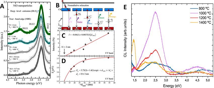
1786 M. Taeño et al.: Emerging optical and optoelectronic applications based on NiO
Table : Values of dielectric constant (ε), refractive index (n), and where two Ni2+ (NixNi ) react with oxygen to produce one
plasma frequency (ωp) from NiO, extracted from Ref. []. ″
ionized nickel vacancy (VNi ) and two Ni3+ (NiNi) ions in the NiO
crystal. Each created Ni3+ ion, acts as a donor which donates a
RF Power ε n ωp (s−) ×
hole, confirming the p-type conductivity of this oxide.
W . . . Over the last years, NiO micro and nanostructures have
W . . .
demonstrated significant applicability in a wide range of
W . . .
research fields, including spintronics, supercapacitors,
fuel cell electrodes, photocatalysis, chemical gas sensors,
or magnetic devices, among others [12–16]. The high
However, its conductivity can be improved by increasing transparency in the visible range of this wide band gap
the concentration of nickel vacancies and oxygen in- material, together with its large hole conductivity and high
terstitials, either by a controlled synthesis or by appro- charge carriers mobility make NiO a suitable option for
priate doping. For example, Napari et al. [6] reported the optoelectronic devices. Among these applications, NiO is
growth of NiO thin films following a plasma-enhanced recognized of prime choice in electrochromic devices and
atomic layer deposition, which were characterized by Hall smart windows [17, 18], in which NiO is extensively used as
effect measurements. The results showed resistivity values anodic colouring material. The electrochromic behaviour
in a range between 80 and 200 Ω/cm as a function of the of this transition metal oxide is based on the colour
film thickness, measured using a van der Pauw configu- changes related to the variations in the oxidation state of
ration. These films were confirmed to have p-type con- the Ni ion under an applied bias. Over the last years, the use
ductivity, with a carrier concentration around 1017 cm−3 and of this transition metal oxide in photovoltaic devices is
mobility close to 0.1 cm2/Vs. Following a similar proced- attracting great interest as well. To date NiO is claimed to be
ure, Diao et al. [7], synthesized Li doped NiO thin films with a promising candidate to be used in emerging perovskite
different annealing temperatures and times by a modified solar cells [19, 20], where it is mainly used as a hole
spray method. Li doped NiO films exhibited a p-type con- transport layer. Besides, NiO has been also employed in
ductivity with resistivities between 4.73 and 1.08 Ω/cm, p-type dye sensitized solar cells (DSSC) [21], in which the
carrier concentrations between 1014 and 1017 cm−3 and normal principle of the common n-type DSSC is inverted, as
mobilities between 2.39 and 11.96 cm2/Vs. The p-type well as in tandem photovoltaic devices based on its com-
behavior has been also observed in Sn-doped three bination with other n-type oxides [22]. Indeed, p–n heter-
dimensionally ordered macroporous NiO, as confirmed ojunction based on p-type NiO and well-known n-type
Wang et al. [8]. In this case, the carrier concentrations oxides such as ZnO and TiO2 have been also developed as
varied from 4.78 × 10¹⁶ to 8 × 1012 cm−3 and mobilities were photodiode heterojunctions with demonstrated applica-
found from 1.31 to 662.25 cm2/Vs. For all the cases, the bility as photodetectors [23, 24]. Although p-type solar cells
improvement in the conductivity is associated to a non- have been widely exploited, the maximum photo-
stoichiometry of NiO promoted by dopants incorporation conversion efficiency (PCE) is still lower in comparison
and/or different synthesis conditions, which enhance the with other n-type semiconducting oxides such as SnO2,
characteristic low conductivity of stoichiometric NiO. The ZnO or TiO2 among others. For example, dye-sensitized
origin of the p-type conductivity of NiO is related to the solar cells (DSSCs) have reached a mature stage with PCE
formation of interstitial oxygen [9, 10] and the inherent over 14% for n-type cells [25], while p-type DSSCs have
nickel deficiency, which motivates its extended use as hole reached moderate PCEs of up to 2.5% [26]. In this context,
transport material in optoelectronic devices. NiO, usually inorganic–organic halide perovskite solar cells (PSCs)
exhibits an oxygen excess accommodated by nickel va- have received attention in the last years due to the signif-
cancies. Both, theoretical and experimental results have icant increase in power conversion efficiency, from 3.8% in
shown that the formation energy of Ni vacancies is the 2009 to 25.2% recently [27]. In the interest of improvement
lowest for all the defects, leading to p-type conduction of these devices, it is important to select an efficient hole
[5, 6]. Moreover, the intrinsic nickel deficiency is usually transport layer material, being NiO one of the most studied
accompanied by the formation of Ni3+ in order to reach p-type oxides. The large bandgap and the deep-lying
charge neutrality [11]. The nickel vacancies created at the valence band that cause favourable energy level alignment
cation sites can be ionized to create Ni3+ following the with the perovskite active layer, makes NiO a promising
reaction: candidate for these devices [27]. Recently, Kim et al. [27]
″
reported a photoconversion efficiency of a PSC with NiO
2NixNi + 1/2 O2 → 2NiNi + OxO + VNi deposited by thermal evaporation around 17% with open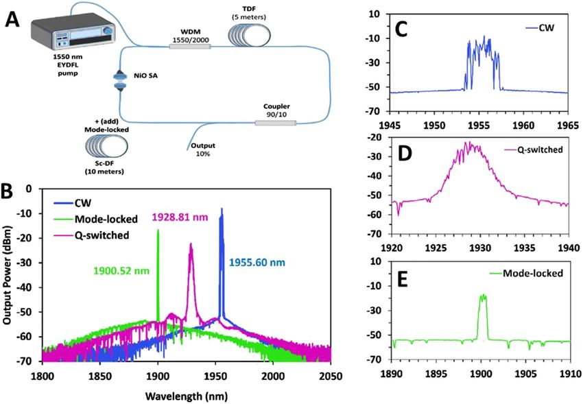
M. Taeño et al.: Emerging optical and optoelectronic applications based on NiO   1787

circuit voltage 1.07 V, short circuit current density of          controlled achievement of low dimensional NiO with spe-
20.68 mA/cm2 and a fill factor of 75.51%. To date, the use of      cific dimensions, morphology, composition and physico-
NiO as hole transport material is replacing common                chemical properties. In some cases, their development and
organic compounds such as PEDOT:PSS, as the stability             integration in diverse optical and optoelectronic devices
and hydrophobic nature of the former provides lower               are yet not resolved. Reducing the size to the microscale
degradation under high temperature and ambient moisture           and nanoscale often offers advantages and novel applica-
conditions. Furthermore, increased attention is gained by         bility for NiO by improving the properties and/or adding
the use of NiO as a hole transport material in quantum dot        new ones, thus allowing to explore novel functionalities.
solar cells (QDSCs), as recently reported for QDSCs based         Different approaches have been explored so far for the
on PbS, Si, and N doped carbon quantum dots, among                synthesis of NiO micro- and nanostructures in order to
others [28, 29].                                                  adequate its characteristics to the required performances,
     It is remarkable that despite the appealing merits of        which usually demand NiO with improved conductivity,
NiO to be used in optical and optoelectronic applications,        specific defects and impurity levels in the bandgap, as well
this versatile material still lags in performance in these        as particular dimensions. Furthermore, the design of op-
fields of research. Actually, the number of research works        tical devices usually requires a high control of the
reporting on NiO-based optical applications is scarce so          morphology and size of the NiO micro- and nanostructures,
far, although over the last years a growing number of high        which can be used as building blocks in diverse optical and
impact scientific research point out to the promising             optoelectronic devices. Either chemical or physical routes
applicability of NiO in diverse optical devices. This interest    have been employed so far in order to achieve an improved
gives birth to the development of emerging research lines         functionality of this transition metal oxide. It is well-known
based on the applicability of NiO low dimensional struc-          that numerous synthesis techniques have been employed
tures as an optical and optoelectronic material.                  in the last decades to deposit NiO thin films. Among these,
     Some of the recent developments on NiO-optical de-           spin-coating [32], spray pyrolysis [33], thermal evaporation
vices are based on the inherent optical nonlinearities of         [27], RF sputtering [34], and DC reactive magnetron sput-
this material, associated with d–d transition levels and          tering [35] have been commonly reported. By controlling
oxygen deficiency [30, 31], while some other applications          experimental conditions such as oxygen flow rates, thick-
exploit the opto-electronic properties of NiO. However,           ness of the deposited NiO films or doping processes, the
there are optical approaches in which the use of NiO still        most relevant physical properties of NiO can be tailored.
remains less explored despite its potential applicability.        The need to overcome the actual limitations of thin films for
New perspectives to develop optical power limiters, optical       their implementation in some devices, has led to the search
switches, ultrafast photonic devices, photodetectors, op-         of new strategies and synthesis methods which allow to
tical resonators, lighting devices, or waveguides based on        obtain low dimensional micro- and nanostructures. Hence,
NiO have been recently explored, thus confirming the great         in addition of the extended synthesis of NiO in form of thin
interest aroused by NiO in the optic and optoelectronic           films, it has been only recently that more variable and
fields in which there is still room for improvement.               complex morphologies have been also reported in
     This review is focused on less explored and emerging         response to modern technological demands. Low dimen-
optical and optoelectronic applications based on NiO mi-          sional NiO in forms of nanorods, wires, belts, sheets, tubes,
cro- and nanostructures. Recent scientific works reporting        or more complex morphologies such as flower-like struc-
on the promising applicability of NiO in light emitting di-       tures and microcrystals with grid-pattern surfaces have
odes and lighting devices, optical resonators, waveguides,        been fabricated by means of different techniques. For the
saturable absorbers, and neuromorphic applications,               fabrication of the NiO nanoparticles, mainly chemical
where dimensions, morphology, and composition, play a             routes have been followed, such as hydrothermal method,
key role, are reviewed.                                           hydrolysis, sol–gel, or coprecipitation methods [3, 36, 37].
                                                                  For the fabrication of elongated structures and more
                                                                  complex morphologies, synthesis techniques such as
                                                                  electrospinning, thermal oxidation, spray pyrolysis or
2 Synthesis of NiO micro- and                                     chemical vapor deposition techniques are commonly
  nanostructures                                                  employed [38, 39]. Moreover, in order to achieve environ-
                                                                  mental clean, safe and affordable synthesis methods,
The advent of novel NiO based optical devices requires            green chemistry synthesis of NiO is recently gaining great
to face scientific and technological challenges, as the            attention [40].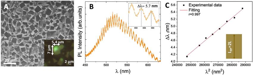
1788          M. Taeño et al.: Emerging optical and optoelectronic applications based on NiO

     Some examples of low dimensional NiO structures                     image in Figure 1G shows a Sn doped NiO surface with grid
fabricated following different synthesis routes are shown                patterning as well as microwires some microns length
in Figure 1. NiO nanoparticles with dimensions between 8                 grown by a vapor–solid process at 1400 °C assisted by Sn
and 22 nm synthesized by a sol–gel method are shown in                   doping [38]. This route allows to obtain new morphologies
the TEM image in Figure 1A [41]. Fabrication of elongated                not previously reported for NiO, avoiding the use of cata-
nano- and microstructures are less extended for NiO.                     lysts and therefore reducing the cost of the processes.
Figure 1B shows a TEM image from a NiO nanorod 5 nm                           Doping with different elements not only affects to the
width fabricated by a rapid thermal oxidation under a                    chemical behaviour or surface states [46] but is also a
controlled oxygen atmosphere using Au as a catalyst [39].                common strategy to tailor the physico-chemical proper-
A submicrometric NiO hollow sphere synthesized by spray                  ties of this transition metal oxide and to achieve improved
pyrolysis followed by a subsequent controlled heat treat-                functionalities. In most cases, the controlled doping
ment is shown in the TEM image in Figure 1C [42]. Porous                 process aims to improve the electrical conductivity and
nanobelts arrays with flake appearance synthesized by                     magnetic response of NiO by modifying the final stoichi-
hydrolysis and etching methods are shown in the Scanning                 ometry, however optical properties can be also tailored by
Electron Microscope (SEM) image in Figure 1D [43]. SEM                   controlling the synthesis process and post treatments.
image in Figure 1E shows a rose-like NiO microstructure                  Incorporation of dopants with diverse oxidation states in
formed by nanoplates synthesized by a solvothermal                       NiO could lead to variations in the concentration of Ni
method combined with a calcination process [44]. Vapor–                  vacancies as well as a tuned Ni2+/Ni3+ ratio in order to
solid processes have been recently used for the growth of                reach charge neutrality. In addition, the incorporation of
NiO micro- and nanostructures. The NiO microcrystals with                impurity levels in the bandgap can also lead to variable
a labyrinth appearance shown in Figure 1F were fabricated                luminescence and tuned optical performance. Diverse
following a one-step vapor process method at 1200 °C using               elements of technological interest, such as Li, Cu, Sn, Co,
metallic Ni as precursor and a controlled Ar flow [45]. SEM               Al, and K, among others, have been used as dopants in

Figure 1: (A) NiO nanoparticles synthesized by sol–gel reproduced from Ref. [41] with permission from the Royal Society of Chemistry. (B) NiO
nanorod fabricated by thermal oxidation using Au as a catalyst reproduced from Ref. [39], (C) NiO hollow sphere synthesized by spray pyrolysis
reprinted with permission from Ref. [42] Copyright 2018 American Chemical Society. (D) NiO nanobelts synthesized by hydrolysis reproduced
with permission from [43]. Copyright (2015) Wiley. (E) Flower-like NiO synthesized by a solvothermal route reprinted from Ref. [44] Copyright
2015, with permission from Elsevier. (F) Labyrinth-like NiO microcrystals fabricated by a vapor-solid process reprinted with permission from
Ref. [45] Copyright 2020 American Chemical Society. (G) Sn doped NiO grid-patterning and microwires grown by a vapor-solid method
reprinted from Ref. [38] Copyright 2020, with permission from Elsevier.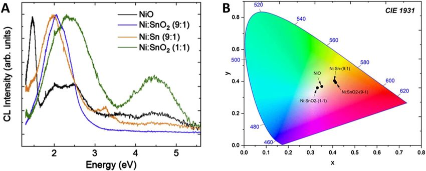
M. Taeño et al.: Emerging optical and optoelectronic applications based on NiO   1789

NiO as a function of the required improved performance          oxygen vacancies or interstitials can be also promoted by
[38, 47–50].                                                    controlling the experimental conditions.
                                                                     As some examples related to the luminescent proper-
                                                                ties of NiO, Figure 2A shows the PL spectra from NiO
3 Optical and optoelectronic                                    nanoparticles synthesized by a sol–gel method acquired
                                                                using a UV laser of 266 nm (4.66 eV) as excitation source
  applications based on NiO                                     [36]. According to the authors, in this case, the lumines-
                                                                cence of the NiO nanoparticles is dominated by a deep-
In this section, emerging NiO-based optical and optoelec-       level green emission around 520 nm (2.38 eV) together with
tronic applications will be reviewed, with special attention    a weak near band edge emission in the UV range at 333–
paid to the recent developments of lighting devices, optical    357 nm (3.47–3.72 eV). Structural defects, such as oxygen/
microresonators, waveguides, optical limiters and neuro-        nickel vacancies and interstitials are related with the green
morphic devices based on NiO micro- and nanostructures.         emission, while the UV emission is due to excitonic re-
                                                                combinations corresponding to near band-edge transitions
                                                                in NiO. A scheme showing the different emissions and the
3.1 Lighting devices                                            related electronic transitions is also depicted in Figure 2B,
                                                                together with the dependence of the UV emission
As a wide bandgap material, NiO can exhibit broad               (Figure 2C) and the band gap energy (Figure 2D) as a
luminescence from the near infrared to the ultraviolet          function of the crystallite dimensions. In addition to the UV
range based on the different recombination levels in the        and green emissions previously described, additional
bandgap. The study of the NiO luminescence allows               contributions can be observed after the deconvolution of
achieving deeper comprehension of the formation of de-          the PL spectra. The violet emission at 2.97 eV appeared
fects during the synthesis, doping and post treatment of        through the possible transition of trapped electrons at Ni
the NiO samples, leading as well to improved perfor-            interstitial to the valence band. The blue luminescence
mance in diverse optical applications. Despite the po-          peak at 2.70 eV is associated to radiative recombination of
tential interest of the NiO luminescence, not many works        electrons from the doubly ionized Ni vacancies to the holes
reported on the luminescence of this material so far. To        in the valence band. Taking this into account, the structure
date, mainly photoluminescence (PL) studies have been           of defects in NiO can be modified by the selected synthesis
developed, together with a few studies based on the             route and post-treatments, as well as by doping, leading to
cathodoluminescence (CL) and electroluminescence (EL).          variable luminescence, as reported by different authors
Luminescence from NiO is commonly associated with Ni            [48]. Some works report on the PL signal from NiO nano-
deficiency, d–d transitions and defect or impurity levels       material using lasers with different wavelengths, however,
in the bandgap. However, diverse luminescence infor-            less has been done so far in the study of the CL signal, a
mation can be achieved as a function of the selected            technique which can shed light to the deeper comprehen-
luminescence technique.                                         sion of the levels in the bandgap. Recently, Taeño et al. [45]
    The optical properties, and therefore the electronic        reported a complete CL study of NiO samples as a function
band structure of NiO can be modulated by the size or the       of the sintering temperature. In that study, diverse NiO
presence of dopants in this metal transition oxide [51].        microstructures were fabricated at temperatures between
Manikandan et al. [52], reported that for stoichiometric NiO    800 and 1500 °C under a controlled Ar flow using metallic
synthesized using a microwave combusting method, only           Ni as precursor material. Figure 2E shows the variable CL
emissions in the UV region (346 nm) can be observed,            emissions acquired at 110 K from the NiO samples as a
which should correspond to a near band-edge emission            function of the sintering temperature. This CL signal covers
due to the recombination of excitons. This fact confirms         a broad range of energy from the near IR (1.49 eV), to the
that the presence of defects in NiO promoted by several         visible (1.96, 2.22, and 2.55 eV), and the UV (4.43 eV). Both
factors, plays a key role in the luminescence properties and    the intensity and the shape of this signal can be tailored as
therefore in the optical applications of this oxide. Ther-      a function of the defects promoted or quenched during the
modynamically, it is found that nickel vacancies are the        thermal annealing. The complex emission in the visible
most dominant point defects present in NiO, therefore the       range 2–2.5 eV is mainly associated with the presence of
optical properties of this oxide should be dominated by the     nickel vacancies, confirmed by the presence of Ni3+, while
radiative emissions promoted for the presence of Ni va-         the near-IR emission is due to transitions involving 3d
cancies. However, the presence of other defects such as         energy levels. High energy emissions in the CL spectrum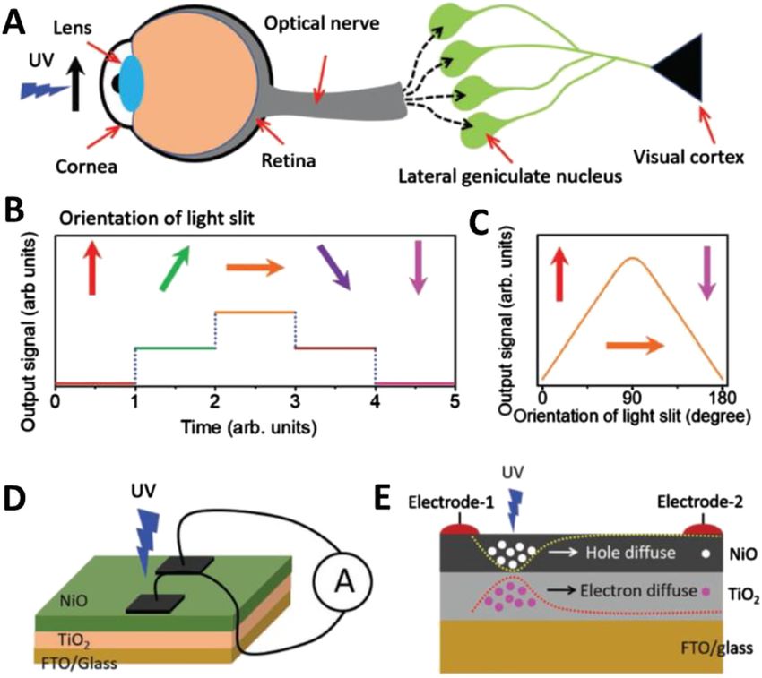
1790          M. Taeño et al.: Emerging optical and optoelectronic applications based on NiO

Figure 2: (A) Photoluminescence (PL) spectra from NiO showing dependence with the crystallite size. (B) Proposed electronic transitions
between defect levels and bandgap of NiO nanoparticles. (C) Intensity of the UV emission and (D) bandgap energy as a function of the
nanoparticles size, reproduced from Ref. [36]. (E) CL spectra acquired at 110 K from NiO samples sintered at 800, 1000, 1200 and 1400 °C.
Reprinted with permission from Ref. [45] Copyright 2020 American Chemical Society.

are related to d–d charge transfer excitons in NiO and near            NiO microstructures covers a wide range of energies, with
band edge emissions. Luminescence from NiO can be also                 emissions in the near-IR (1.46 eV), the visible (2–2.5 eV) and
tuned by appropriate doping, however in order to face                  the UV range (3.5 and 4.5 eV), the relative intensity of which
potential functionalization in luminescent devices the                 can be tuned as a function of the composition of the pre-
inherent low luminescent intensity from NiO should be                  cursor mixture, as shown in Figure 3A. Appropriate Sn
overcome. In a recent work, Taeño et al. [38] reported an              doping can also tune the NiO luminescence from the near-
increase of the luminescence signal from NiO by Sn doping.             IR to the UV. The chromaticity diagram obtained from the
In this case, the CL signal from Sn doped NiO samples                  CL spectra in Figure 3A is shown in Figure 3B.
fabricated by thermal treatments at 1400 °C can be                          Similarly to other metal oxides, modulation of the NiO
increased in a factor ×40 by low Sn doping. In that work,              luminescence can be achieved by controlling the synthesis
different Sn-based precursors in a variable concentration              method, the doping process as well as by treatments under
were used for the achievement of the Sn doped NiO nano-                diverse atmospheres. Hence, either monochromatic or
and microstructures in forms of grid-self assembled com-               wide luminescence can be obtained as a function of the
plex surfaces and microwires. The luminescence of these                requirements for the NiO based luminescent device. The

Figure 3: (A) Normalized cathodoluminescence (CL) spectra from NiO and Sn doped NiO samples grown at 1400 °C using different precursors
and (B) CIE 1931 chromaticity coordinates from spectra in (A). Reprinted from Ref. [38] Copyright 2020, with permission from Elsevier.
M. Taeño et al.: Emerging optical and optoelectronic applications based on NiO              1791

capability of emitting broadband white light also reveals                 the oxides properties, and insertion of organic layers. In
promising applicability of NiO in white-light emitters                    recent years, Q-LEDs have attracted increasing interest as
without the need of phosphors or quantum well structures.                 these devices demonstrated high fluorescence efficiency,
     Based on the excellent optoelectronic properties of                  long fluorescence life, and large luminosity. Furthermore,
NiO, it has been also considered as a great candidate in                  Q-LEDs can exhibit adjustable emission spectrum as a
light-emitting-diodes (LEDs), as a constituent of a p–n                   function of the bandgap width of the quantum dots (QD).
heterojunction, and more recently in quantum-dot LEDs                     Indeed, Q-LEDs are expected to be one of the most prom-
(Q-LEDs) and organic–inorganic hybrid LEDs (Hy-LEDs).                     ising candidates in the next generation lighting devices.
The characteristic high work function and large ionization                The singular optoelectronic properties of NiO make it
energy of this p-type oxide, as well as its good stability and            useful for hole transport and electronic barrier material in
carrier transport performance, make it an excellent                       these devices. In order to overcome some of the electronic
candidate to be exploited in solid state lighting devices, as             drawbacks which could hinder the applicability of NiO,
demonstrated in recent scientific works. It should be noted                doping with different elements was employed to improve
that the achievement of reliable p-type doping in most                    its hole mobility and conductivity, thus leading to
semiconducting oxides such as Ga2O3, ZnO, SnO2, In2O3,                    enhanced current efficiency. Zhang et al. [37] reported the
and TiO2 is a difficult and controversial task which hinders               synthesis of Fe doped NiO nanocrystals by a solvothermal
the development of homojunction LEDs and other optical                    route used as a hole injector layer in a Q-LED with
devices. Therefore, an alternative strategy is to fabricate p–            competitive results. Enhanced fluorescence intensity was
n heterojunctions by integrating n-type and p-type semi-                  achieved in this case by increasing Fe doping, mainly due
conducting oxides if the interface quality is controlled in a             to passivation of the surface defect states of NiO and a
proper manner. Among the p-type oxides, NiO arouses                       decrease of the exciton quenching effect on the quantum
increased interest due to its optimal electro-optical prop-               dot light emitting layer. Figure 4B shows the current effi-
erties and stability, which motivates its use in hetero-                  ciency as a function of the luminance for different Fe
junction LEDs based in oxide materials. As some examples,                 doping in the Fe doped NiO based Q-LEDs. By 5 mol% Fe
Xi et al. [53] reported on the fabrication of a p-type NiO/               doping in NiO, enhanced carrier concentration and elec-
n-type ZnO based LED using low temperature solution-                      trical conductivity were achieved. Maximum values of
based growth methods. In that case, the initial negligible                luminescence, quantum efficiency (3.84%) and current
light emission from the as-grown NiO film was improved by                  efficiency (5.93 cd/A) were achieved for the Q-LED showing
annealing. The electroluminescence signal depends on the                  long lifetime of 11,490 h. Inset in Figure 4B shows the
bias voltage, leading to intense UV emission for high bias                excellent monochromacity of one red QLED based on Fe
voltages. Figure 4A shows the I–V curves of different de-                 doped NiO at an applied voltage of 5 V.
vices based on the NiO/ZnO system with variable layers,                        NiO has been also used as hole injection layer in
where a diode-like behavior can be observed for all the                   organic–inorganic hybrid LEDs (Hy-LEDs). The low cost,
devices. Despite the low efficiency exhibited by these de-                 scalability and mechanical properties of these hybrid LED
vices (maximum emission power 0.14 μW/cm2 at 23 V bias)                   make them interesting candidates in solid state lighting
it could be easily improved by optimized design, tuning of                devices and flexible-display technologies [47, 54]. In a

Figure 4: (A) I–V curves from the different heterojunction devices, reprinted from [53] with permission of AIP publishing. (B) Current efficiency
versus luminance of the Q-LEDs. The inset in (B) shows a digital photograph of the c-based Q-LED under a 5 V applied voltage. Reprinted from
Ref. [37] Copyright 2020, with permission from Elsevier. (C) Current density–voltage–luminance curves of the hybrid LEDs (Hy-LEDs) –
reprinted with permission from Ref. [47] Copyright 2018 American Chemical Society.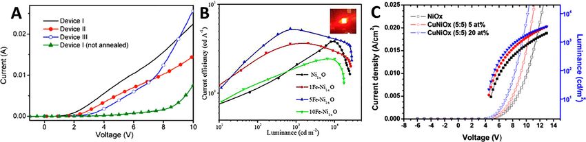
1792           M. Taeño et al.: Emerging optical and optoelectronic applications based on NiO

recent work, Kim et al. [47] reported on the use of Cu (I) and              3.2 Optical resonators and waveguides
Cu (II) codoped NiO films synthesized by sol–gel which
exhibit high ionization energy, as well as improved con-                    The applicability of NiO as building blocks in some optical
ductivity and hole injection ability due to the large amount                devices requires the fabrication of low dimensional struc-
of Ni vacancies promoted by Cu co-doping. In that case, an                  tures with improved optical properties and well-defined
improved performance was achieved for the Cu codoped                        dimensions and morphology, which in some cases involves
NiO films, as compared with pristine NiO. Figure 4C shows                    the upgrade of the synthesis methods. Over the last years,
the current density–voltage–luminance curves both from                      the development of low dimensional optical microcavities
pristine NiOx and Cu codoped NiO based devices. It can be                   has aroused great attention as they can be used in devices
clearly observed that both the current density and the                      in which light confinement is required, such as lasers,
luminance increase for the Cu codoped NiO based devices,                    optical resonators, filters, and waveguides, among others.
based on an enhancement of the hole density in the emit-                    In this frame, some authors reported on the use of different
ting layer. Moreover, the NiO-based hole injection layer                    semiconducting oxides microstructures with variable
induces a well-balanced electron and hole charge injec-                     morphologies in form of microtubes and microrods with
tion. A current efficiency of 15.4 cd/A at 500 cd/m2 was                     hexagonal or rectangular cross-sections, as low dimen-
achieved for the Hy-LED with 5 at.% Cu codoped NiOx,                        sional optical resonators in which Fabry–Perot (FP) reso-
which in this case shows a maximum of the electrolumi-                      nances due to light reflections between the opposed flat
nescence signal in the green range (510 nm).                                ends of the cavity and/or whispering gallery modes (WGM)
     As previously mentioned, NiO has been also employed                    involving total internal reflections around the inner faces
as a constituent in p–n heterojunctions diodes. Recently,                   of the cavity can occur [57–59]. However, despite the po-
Gong et al. [55] constructed NiO/β-Ga2O3 p–n hetero-                        tential applicability of NiO in these types of optical devices,
junctions diodes by a double layer design of NiO with                       it has been only recently that NiO-based resonant cavity
varied hole concentrations. According to the authors, by                    modes have been reported [60, 61]. In that work, FP modes
reducing the hole concentration from 3.6 × 10¹⁹ to                          were observed in the visible range and analyzed for NiO
5.1 × 1017 cm−3, the leakage current density is reduced to                  microcrystals with lateral dimensions around 10 µm
10−9 A/cm2 while a high rectification ratio over 1010 is still               fabricated by thermal treatments at 1200 °C (Figure 5A).
maintained even operating at high temperature of 400 K.                     Light confinement and optical resonances are favoured by
The results showed that the resultant device possesses a                    the singular geometry, flat and well-faceted surfaces and
record high breakdown voltage (Vb) of 1.86 kV compared                      high crystalline quality of the as-grown NiO microstruc-
with other β-Ga2O3 based p–n heterojunction diodes [56].                    tures. Among the probed microcrystals, only those with
The improvement breakdown voltage is attributed to the                      smooth surfaces exhibit clear modulations in the corre-
suppression of electric field crowding by decreasing hole                    sponding photoluminescence spectrum acquired with an
concentration in NiO.                                                       UV laser (λ = 325 nm), as shown in Figure 5B which

Figure 5: (A) Scanning Electron Microscope (SEM) image from NiO microcrystals. Inset in (A) shows an optical image from a detailed region
with NiO microcrystals. (B) Photoluminescence (PL) spectrum from the microcrystal in the inset in (A) showing optical modulations, enlarged in
the inset. (C) Δλ versus λ2 from the analysis of the PL signal in (B) with the corresponding linear fitting. Reprinted from Ref. [60] Copyright 2021,
with permission from Elsevier.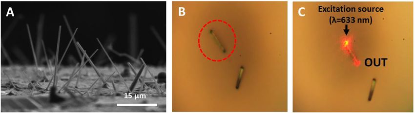
M. Taeño et al.: Emerging optical and optoelectronic applications based on NiO 1793
corresponds to the microcrystal shown in the optical image reported for NiO, to the best of our knowledge. Figure 6B
included as an inset in Figure 5A. A detailed analysis of the shows an optical image from the Sn doped NiO microwires
modulated signal and the mode spacing, included in deposited onto a silicon substrate while Figure 6C shows
Figure 5C, indicated that the NiO microcrystals behave as the bright field optical image in which a waveguiding
Fabry–Perot optical microcavities, although the presence behaviour can be observed in the marked microwire. When
of WGM cannot be disregarded. An experimental refractive the microwire is illuminated by one end a bright signal
index of n = 2.3 ± 0.2 was also obtained from the analysis of light can be observed in the opposite end, thus confirming
the resonances observed in the NiO microcrystals. Besides, the waveguiding behavior.
quality (Q) and finesse (F) factors around 207 and 1.8,
respectively, were calculated for the microcavities, which
can be further improved by an exhaustive control of the 3.3 Optical limiters and biomedical
morphology and dimensions of these NiO microstructures. applications
Moreover, a method for the fabrication of a platform with
multiple NiO based optical resonators is proposed, avoid- Among the emerging optical functionalities based on the
ing complex post treatments or single structures manipu- multifunctional photonic properties of NiO, recent ad-
lation [61]. vances have been reported on its use as optical limiter,
As previously mentioned, the fabrication of NiO elon- saturable absorber and optical switch. Over the last years,
gated microstructures has not been deeply explored so far. optical limiting devices exhibited large applicability as
However, based on preliminary works, NiO elongated optical switches, mode lockers, and optical safety. Actu-
structures with different morphology and dimensions can ally, in order to avoid potential damage under intense laser
be obtained as a function of the experimental conditions condition, the use of appropriate optical limiters is
and Sn-based precursor. As an example, Figure 6A shows a mandatory in photonic sensors, including the human eye
SEM image of Sn doped NiO microwires obtained following as well. Furthermore, the passive saturable absorbers
a vapor–solid method at 1400 °C using metallic Ni and SnO2 exhibit advantages in the fabrication of Q-switching and
as precursors materials. The growth of these microwires is mode-locking pulses, as compared with other active tech-
favoured by the presence of Sn-based compounds in the niques, mainly due to the low cost and easy fabrication of
precursor mixture. When using a mixture of metallic Ni and the formers.
SnO2, the as-grown microwires show smooth surfaces and The inherent optical properties of NiO, such as the
regular cross sections, with lengths of tens of µm and suitable wide bandgap and low saturation intensity, make
widths of a few microns, as shown in Figure 6A. The sin- this material a promising saturable absorber mainly
gular geometry and dimensions of these NiO microwires around the 2 µm spectral region. It should be noted that the
could favour their applicability as building block in optical use of fiber lasers operating in the midinfrared spectral
devices. Moreover, these microwires exhibit waveguiding region (∼2 µm) is required in applications including tele-
behaviour, as the light from a He–Ne red laser (633 nm) can communications, medical surgery, and light detection and
be guided along the microstructure without large losses, ranging. Besides, many advantages can be achieved in this
which can wide the optical applicability of NiO. It should spectral range as falls into the “eye-safe laser” category
be noted that this behaviour has not been previously [62]. As an example, thulium and holmium based active
Figure 6: (A) Scanning Electron Microscope (SEM) image from NiO microwires fabricated using Ni and SnO2 in the starting mixture. (B) Optical
images from the NiO microwires placed onto a Si substrate and (C) bright field image from Ni:SnO2 microwire showing waveguiding behaviour
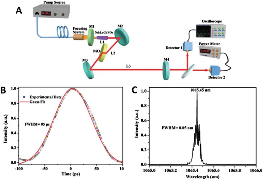
under a red laser illumination.1794 M. Taeño et al.: Emerging optical and optoelectronic applications based on NiO fibers are suitable for ultrashort pulses generation and to absorber, a laser peak shifting is also observed, due to the fabricate lasers with wideband wavelength tuning. changes in the cavity loss. Recently, Rusdi et al. [63] reported the fabrication of Besides, further improvements in the design of optical Q-switching and mode-locked fiber lasers operating in the devices could be achieved by the controlled electron spectral range ∼2 µm using a saturable absorber film based transition processes and the corresponding tuned optical on NiO nanoparticles synthesized by a sonochemical properties of NiO. As a recent example, Sun et al. [64] re- method. The proposed set up for the thulium doped fiber ported the use of NiO nanosheets as saturable absorber in laser is shown in Figure 7A. Figure 7B shows the output ultrafast lasers. The authors synthesized NiO nanosheets spectrum of the laser, at the corresponding threshold with dimensions around 150–200 nm following a hydro- powers, operating at different regimes: continues wave thermal method and describe their optical behaviour (CW), Q-switching and mode-locking modes, as well as which can be tailored as a function of the thickness of the enlarge details of each individual spectrum. It can be nanosheets, leading to saturable and reverse saturable observed how the CW laser transits into Q-switched by absorption, as a function of the intra-band transitions inserting the NiO saturable absorber. Without NiO in the balanced processes. In this case, NiO nanosheets with cavity, the CW laser is stablished centered at 1955.60 nm optimized thickness have been employed as a broad opti- (Figure 7C). When the pump power raises, the CW laser cal modulator based on their saturable absorption effect. transits into Q-switched peaked at 1928.82 nm, which Diode-pumped broadband mode-locked lasers with shows a broader profile (Figure 7D). At higher pump power, wavelengths of 1.06 and 1.34 µm were developed based on selfgenerated mode-locked centered at 1900.52 nm can be a NiO sample optimized for saturable absorption, as observed (Figure 7E). It should be noted that as the pump schemed in Figure 8A. Figures 8B shows the mode-locked power is raised the number of laser modes increases as pulse with a Gaussian profile, while the spectrum in well. As a result of the insertion of the NiO saturable Figure 8C shows the output spectrum centered at 1.06 µm Figure 7: (A) Scheme of the thulium doped fiber laser. (B) Output spectra of the continues wave (CW), Q-switched and mode locked fiber laser at the respective threshold pump powers. Each detailed spectrum is shown in (C), (D), and (E). Reprinted from Ref. [63] Copyright 2019, with permission from Elsevier.
M. Taeño et al.: Emerging optical and optoelectronic applications based on NiO           1795

Figure 8: (A) Experimental configuration of diode pumped mode-locked laser using NiO as saturable absorber. (B) Single pulse and (C) output
spectrum centered at 1.06 µm from a mode-locked laser using NiO nanosheets as saturable absorber. Reproduced with permission from [64],
Copyright (2017) Wiley.

                                                                                               Figure 9: (A) Scheme of the operation of the
                                                                                               human eye. (B) Variation in the output
                                                                                               response of the visual cortex as a function
                                                                                               of the light orientation and (C) Light
                                                                                               orientation-dependent response. (D) Pro-
                                                                                               posed NiO/TiO2 heterostructure with two
                                                                                               planar contacts under UV illumination. (E)
                                                                                               Lateral photocurrent due to the generation
                                                                                               of e–h pairs by illumination near electrode 1
                                                                                               and charge carriers diffusion towards elec-
                                                                                               trode 2. Reproduced with permission from
                                                                                               [65] Copyright (2019) Wiley.
1796 M. Taeño et al.: Emerging optical and optoelectronic applications based on NiO
with a full-width half-maximum of 0.05 nm at the central marked in Figure 9E, leading to the generation of lateral
wavelength. photocurrent. In addition to lateral photovoltaic genera-
As a proof of the versatility of NiO, this material is tion and photoresponse dependent on the orientation, this
earning a place among biomedical optics, as recently re- device also exhibits switching behaviour with rise and fall
ported by Kumar et al. [65] which developed a NiO-based times of 3 and 6 ms, respectively. This self-biased device
optical device that mimics the primitive functions of the with orientation dependent response could pave the way to
visual cortex. At the forefront of the neuromorphic appli- the development of artificial visual systems.
cations, including artificial visual processing, the devel-
opment of optoelectronic devices emulating the visual
cortex using optical stimuli under self-biased conditions 4 Conclusions
will play key role in future biomedical optical applications.
Among other requirements, these neuromorphic devices To summarize, recent progress on emerging optical and
should accomplish low processing energy, for which optoelectronic devices based on NiO are reviewed in this
photonic triggered devices operating in self-biased condi- work. This transition metal oxide is one of the very few
tions, as those described by Kumar et al., appear as p-type oxide, which interesting physico-chemical proper-
promising candidates. In this work [65], the authors ties provide wide applicability in diverse fields of techno-
developed a high transparent all oxide NiO/TiO2-based logical research. However, less has been done so far in the
optoelectronic device with brain-like functionalities which development of NiO-based optical and optoelectronic de-
mimics the operation and response of the visual cortex. The vices, despite the potential use of this oxide in the optical
NiO films 30 nm thick were grown as a part of the NiO/TiO2 field. To date, apart from the well-known use of this ma-
heterostructure using a reactive sputtering with a Ni target terial in electrochromic devices and smart windows, where
(99.999% purity). As stated by the authors, the final NiO is of prime choice, as well as a hole injector layer in
micrometric dimensions of the device could be further emerging photovoltaic devices, less has been done so far in
reduced by future advanced photolithography processes. the development of NiO based optical devices. The quest
The operation of the device is based on the generation of a for innovative optical devices requires the use of materials
lateral photovoltaic current under nonuniform illumina- which accomplish novel applicability and improved per-
tion. The input illuminating photons should induce formance. In this regard, over the last years a growing
electron-hole pairs in the heterostructure and lead to a number of high impact research works points out to the
photocurrent collected by two top planar Ag contacts. As potential use of NiO in diverse optical and optoelectronic
the photocurrent outputs correlate with the spatially applications, leading to a young and promising research
distributed optical inputs, the device exhibits orientation line in which there is still room for improvement. The
selective response, which is essential in the achievement of present review comprises an overview of emerging optical
the neuromorphic artificial vision. and optoelectronics applications based on NiO micro- and
The selection of NiO as an active component of this nanostructures. Either undoped and doped NiO nano-
device is not only based on its inherent p-type conductivity, material synthesized by diverse synthesis routes are
but also on its characteristic wide bandgap, which allows included in this work. Firstly, the use of NiO in lighting
high transmittance in the visible range, and its work- devices, including Q-LEDs and Hy-LEDS, is reviewed, with
function which in combination with TiO2 leads to the for- special attention paid to the presence of defects and im-
mation of a separation charge layer leading to the sepa- purity levels in the bandgap and to the enhancement of the
ration of the photogenerated hole-electron pairs and luminescence intensity. Secondly, NiO microstructures in
preventing their recombination. form of microcrystals and microwires fabricated by a va-
Figure 9A shows a scheme of the human eye operation por–solid process are reviewed based on their demon-
where the optical information is transferred to the visual strated use as optical resonators and waveguides. Fabry–
cortex via the optic nerve. The sensitivity to the light Perot modes have been recently described and analyzed in
orientation and the orientation dependent response of the NiO microcrystals. The achievement of these microstruc-
visual cortex are shown in Figure 9B and C, respectively. tures with controlled and well-defined morphology allows
The proposed NiO/TiO2 based device is schemed in their use in optical devices. Thirdly, the use of NiO as
Figure 9D, where two planar contacts collect the current saturable absorber in optical limiter devices and ultrafast
when the UV illumination reaches the surface. The lasers is also described, mainly in the range of ∼2 µm.
photoinduced holes, in NiO, and electrons, in TiO2, diffuse Finally, biomedical optical applications such as a neuro-
laterally from the illuminated electrode 1 to electrode 2, morphic device which mimics the operation and responseM. Taeño et al.: Emerging optical and optoelectronic applications based on NiO 1797
of the virtual cortex is reviewed as well, paving the way to [10] A. N. Banerjee, C. K. Ghosh, and K. K. Chattopadhyay, “Effect of
the development of neuromorphic artificial vision. These excess oxygen on the electrical properties of transparent p-type
conducting CuAlO2+x thin films,” Sol. Energy Mater. Sol. Cells, vol.
emerging optical and optoelectronic NiO-based applica-
89, no. 1, pp. 75–83, 2005.
tions can open a promising field of research based on this [11] X. Xu, L. Li, J. Huang, et al., “Engineering Ni3+ cations in NiO
p-type material where further improvements are still under lattice at the atomic level by Li+ doping: the roles of Ni3+ and
development. oxygen species for CO oxidation,” ACS Catal., vol. 8, no. 9,
pp. 8033–8045, 2018.
[12] R. Kumar, C. Baratto, G. Faglia, G. Sberveglieri, E. Bontempi, and
Author contributions: All the authors have accepted
L. Borgese, “Tailoring the textured surface of porous
responsibility for the entire content of this submitted
nanostructured NiO thin films for the detection of pollutant
manuscript and approved submission. gases,” Thin Solid Films, vol. 583, pp. 233–238, 2015.
Research funding: This work was supported by MINECO/ [13] Y. Ku, C-N. Lin, and W-M. Hou, “Characterization of coupled NiO/
FEDER/M-ERA.Net Cofund projects: MAT 2015-65274-R, TiO2 photocatalyst for the photocatalytic reduction of Cr(VI) in
RTI2018-097195-B-100 and PCIN-2017-106. This research aqueous solution,” J. Mol. Catal. Chem., vol. 349, no. 1,
pp. 20–27, 2011.
has received funding from the European Union’s Horizon
[14] G. Cai, X. Wang, M. Cui, et al., “Electrochromo-supercapacitor
2020 research and innovation programme under Grant based on direct growth of NiO nanoparticles,” Nanomater.
Agreement No. 957225, project BAT4EVER. Energy, vol. 12, pp. 258–267, 2015.
Conflict of interest statement: The authors declare no [15] D. U. Lee, J. Fu, M. G. Park, H. Liu, A. Ghorbani Kashkooli, and
conflicts of interest regarding this article. Z. Chen, “Self-assembled NiO/Ni(OH)2 nanoflakes as active
material for high-power and high-energy hybrid rechargeable
battery,” Nano Lett., vol. 16, no. 3, pp. 1794–1802, 2016.
[16] F. Shahzad, K. Nadeem, J. Weber, H. Krenn, and P. Knoll,
References “Magnetic behavior of NiO nanoparticles determined by SQUID
magnetometry,” Mater. Res. Express, vol. 4, no. 8, 2017, https://
[1] D. P. Dubal, P. Gómez-Romero, B. R. Sankapal, and R. Holze, doi.org/10.1088/2053-1591/aa8674.
“Nickel cobaltite as an emerging material for supercapacitors: an [17] A. Dewan, S. Haldar, and R. Narayanan, “Multi-shelled NiO
overview,” Nano Energy, vol. 11, pp. 377–399, 2015. hollow microspheres as bifunctional materials for
[2] Y. Chen, O. Sakata, R. Yamauchi, et al., “Lattice distortion and electrochromic smart window and non-enzymatic glucose
electronic structure of magnesium-doped nickel oxide epitaxial sensor,” J. Solid State Electrochem., vol. 25, pp. 821–830, 2021.
thin films,” Phys. Rev. B, vol. 95, p. 245301, 2017. [18] S. Jin, S. Wen, M. Li, H. Zhong, Y. Chen, and H. Wang, “Effect of
[3] M. Bonomo, “Synthesis and characterization of NiO the grain size on the electrochromic properties of NiO films,”
nanostructures: a review,” J. Nanoparticle Res., vol. 20, no. 8, Opt. Mater., vol. 109, p. 110280, 2020.
p. 222, 2018. [19] L. Hu, J. Peng, W. Wang, et al., “Sequential deposition of
[4] K. S. Usha, R. Sivakumar, and C. Sanjeeviraja, “Optical constants CH3NH3PbI3 on planar NiO film for efficient planar perovskite
and dispersion energy parameters of NiO thin films prepared by solar cells,” ACS Photonics, vol. 1, no. 7, pp. 547–553, 2014.
radio frequency magnetron sputtering technique,” J. Appl. Phys., [20] W. Chen, Y. Wu, J. Fan, et al., “Understanding the doping effect
vol. 114, p. 123501, 2013. on NiO: toward high-performance inverted perovskite solar
[5] C. Park, J. Kim, K. Lee, S. K. Oh, H. Kang, and N. Park, “Electronic, cells,” Adv. Energy Mater., vol. 8, no. 19, pp. 1–10, 2018.
optical, and electrical properties of nickel oxide thin films grown [21] P. Qin, M. Linder, T. Brinck, G. Boschloo, A. Hagfeldt, and L. Sun,
by RF magnetron sputtering,” Appl. Sci. Converg. Technol., vol. 24, “High incident photon-to-current conversion efficiency of p-type
pp. 72–76, 2015. dye-sensitized solar cells based on NiO and organic
[6] M. Napari, T. N. Huq, T. Maity, et al., “Antiferromagnetism and chromophores,” Adv. Mater., vol. 21, no. 29, pp. 2993–2996,
p-type conductivity of nonstoichiometric nickel oxide thin films,” 2009.
InfoMat, vol. 2, pp. 769–774, 2020. [22] A. Nattestad, A. Mozer, M. K. Fischer, et al., “Highly efficient
[7] C. C. Diao, C. Y. Huang, F. Yang, and C. C. Wu, “Morphological, photocathodes for dye-sensitized tandem solar cells,” Nat.
optical, and electrical properties of p-type nickel oxide thin films Mater., vol. 9, pp. 31–35, 2009.
by nonvacuum deposition,” Nanomaterials, vol. 10, no. 4, p. 636, [23] H. Hakkoum, T. Tibermacine, N. Sengouga, et al., “Effect of the
2020. source solution quantity on optical characteristics of ZnO and
[8] Z. Wang, H. Zhou, D. Han, and F. Gu, “Electron compensation in NiO thin films grown by spray pyrolysis for the design NiO/ZnO
p-type 3DOM NiO by Sn doping for enhanced formaldehyde photodetectors,” Opt. Mater., vol. 108, p. 110434, 2020.
sensing performance,” J. Mater. Chem. C., vol. 5, pp. 3254–3263, [24] H. K. Li, T. P. Chen, S. G. Hu, et al., “Highly spectrum-selective
2017. ultraviolet photodetector based on p-NiO/n-IGZO thin film
[9] A. Mallikarjuna Reddy, A. Sivasankar Reddy, K. S. Lee, and heterojunction structure,” Opt. Express, vol. 23, no. 21, p. 27683,
P. Shreedhara Reddy, “Effect of oxygen partial pressure on the 2015.
structural, optical and electrical properties of sputtered NiO [25] K. Kakiage, Y. Aoyama, T. Yano, K. Oya, J. Fujisawa, and
films,” Ceram. Int., vol. 37, no. 7, pp. 2837–2843, 2011. M. Hanaya, “Highly-efficient dye-sensitized solar cells with1798 M. Taeño et al.: Emerging optical and optoelectronic applications based on NiO
collaborative sensitization by silyl-anchor and carboxy-anchor based supercapacitor,” RSC Adv., vol. 5, no. 18,
dyes,” Chem. Commun., vol. 51, pp. 15894–15897, 2015. pp. 14010–14019, 2015.
[26] I. R. Perera, T. Daeneke, S. Makuta, et al., “Application of the [42] B. Y. Kim, J. W. Yoon, J. K. Kim, Y. C. Kang, and J. H. Lee, “Dual
tris(acetylacetonato)iron(III/II) redox couple in p-type dye- role of multiroom-structured Sn-doped NiO microspheres for
sensitized solar cells,” Angew. Chem., vol. 54, pp. 3758–3762, ultrasensitive and highly selective detection of xylene,” ACS
2015. Appl. Mater. Interfaces, vol. 10, no. 19, pp. 16605–16612,
[27] S. K. Kim, H. J. Seok, D. H. Kim, et al., “Comparison of NiOx thin 2018.
film deposited by spin-coating or thermal evaporation for [43] Y. Zhang, W. Zhang, Z. Yang, et al., “Self-sustained cycle of
application as a hole transport layer of perovskite solar cells,” hydrolysis and etching at solution/solid interfaces: a general
RSC Adv., vol. 10, p. 43847, 2020. strategy to prepare metal oxide micro-/nanostructured arrays for
[28] S. Liu, L. Hu, S. Huang, et al., “Enhancing the efficiency and high-performance electrodes,” Angew. Chem. Int. Ed., vol. 54,
stability of PbS qauntum dot solar cells through engineering and no. 13, pp. 3932–3936, 2015.
ultrathin NiO nanocrystalline interlayer,” ACS Appl. Mater. [44] M. Yao, Z. Hu, Y. Liu, P. Liu, Z. Ai, and O. Rudolf, “3D hierarchical
Interfaces, vol. 12, no. 41, pp. 46239–46246, 2020. mesoporous roselike NiO nanosheets for high-performance
[29] S. Chakrabarti, D. Carolan, B. Alessi, P. Maguire, V. Svrcek, and supercapacitor electrodes,” J. Alloys Compd., vol. 648,
D. Mariotti, “Microplasma-synthesized ultra-small NiO pp. 414–418, 2015.
nanocrystals, a ubiquitous hole transport material,” Nanoscale [45] M. Taeño, J. Bartolomé, L. Gregoratti, P. Modrzynski, D. Maestre,
Adv., vol. 1, pp. 4915–4925, 2019. and A. Cremades, “Self-organized NiO microcavity arrays
[30] P. Baraskar, R. J. Choudhary, P. K. Sen, and P. Sen, “Dispersive fabricated by thermal treatments,” Cryst. Growth Des., vol. 20,
optical nonlinearities and optical path length compensation in no. 6, pp. 4082–4091, 2020.
NiO/Al doped NiO bilayer thin film,” Opt. Mater., vol. 96, [46] Z. Xu and J. R. Kitchin, “Relationships between the surface
p. 109278, 2019. electronic and chemical properties of doped 4d and 5d late
[31] R. Chouhan, P. Baraskar, A. Agrawal, M. Gupta, P. K. Sen, and transition metal dioxides,” J. Chem. Phys., vol. 142, p. 104703,
P. Sen, “Effects of oxygen partial pressure and annealing on 2015.
dispersive optical nonlinearity in NiO thin films,” J. Appl. Phys., [47] M. Kim, C. W. Joo, J. H. Kim, et al., “Conductivity enhancement of
vol. 122, no. 2, p. 025301, 2017. nickel oxide by copper cation codoping for hybrid organic–
[32] V. P. Patil, S. Pawar, M. Chougule, et al., “Effect of annealing on inorganic light-emitting diodes,” ACS Photonics, vol. 5, no. 8,
structural, morphological, electrical and optical studies of nickel pp. 3389–3398, 2018.
oxide thin films,” JSEMAT, vol. 1, no. 2, pp. 35–41, 2011. [48] A. S. Bhatt, R. Ranjitha, M. S. Santosh, et al., “Optical and
[33] V. Ganesh, B. Ravi Kumar, Y. Bitla, I. S. Yahia, and S. Alfaify, electrochemical applications of Li-doped NiO nanostructures
“Structural, optical and dielectric properties of Nd doped NiO synthesized via facile microwave technique,” Materials, vol. 13,
thin films deposited with a spray pyrolysis method,” J. Inorg. no. 13, pp. 1–17, 2020.
Organomet. Polym. Mater., 2021. https://doi.org/10.1007/ [49] C. Wang, X. Cui, J. Liu, et al., “Design of superior ethanol gas
s10904-021-01889-3. sensor based on Al-doped NiO nanorod-flowers,” ACS Sens.,
[34] J. R. Abenuz Acuña, S. Perez, V. Sosa, et al., “Sputtering power vol. 1, no. 2, pp. 131–136, 2016.
effects on the electrochromic properties of NiO films,” Optik, [50] Y. J. Mai, J. P. Tu, X. H. Xia, C. D. Gu, and X. L. Wang, “Co-doped
vol. 231, p. 166509, 2021. NiO nanoflake arrays toward superior anode materials for
[35] P. Salunkhe, A. V. M. Ali, and D. Kekuda, “Investigation on lithium ion batteries,” J. Power Sources, vol. 196, no. 15,
tailoring physical properties of nickel oxide thin films grown by pp. 6388–6393, 2011.
dc magnetron sputtering,” Mater. Res. Express, vol. 7, p. 016427, [51] P. Dubey, N. Kaurav, R. S. Devan, G. S. Okram, and Y. K. Kuo, “The
2020. effect of stoichiometry on the structural, thermal and electronic
[36] A. Gandhi and S. Wu, “Strong deep-level-emission properties of thermally descomposed nickel oxide,” RSC Adv.,
photoluminescence in NiO nanoparticles,” Nanomaterials, vol. vol. 8, pp. 5882–5890, 2018.
7, no. 8, p. 231, 2017. [52] A. Manikandan, J. J. Vijaya, and L. J. Kennedy, “Comparative
[37] Y. Zhang, X. Wang, Y. Chen, and Y. Gao, “Improved investigation of NiO nano- and microstructures for structural,
electroluminescence performance of quantum dot light-emitting optical and magnetic properties,” Physica E Low Dimens. Syst.
diodes: a promising hole injection layer of Fe-doped NiO Nanostruct., vol. 49, pp. 117–123, 2013.
nanocrystals,” Opt. Mater., vol. 107, p. 110158, 2020. [53] Y. Y. Xi, Y. F. Hsu, A. B. Djurišić, et al., “NiO/ZnO light emitting
[38] M. Taeño, D. Maestre, and A. Cremades, “Fabrication and study diodes by solution-based growth,” Appl. Phys. Lett., vol. 92,
of self-assembled NiO surface networks assisted by Sn doping,” no. 11, p. 113505, 2008.
J. Alloys Compd., vol. 827, p. 154172, 2020. [54] Y. Wang, Q. Niu, C. Hu, et al., “Ultrathin nickel oxide film as a hole
[39] K. Koga, and M. Hirasawa, “Gas-phase generation of noble buffer layer to enhance the optoelectronic performance of a
metal-tipped NiO nanorods by rapid thermal oxidation,” Mater. polymer light-emitting diode,” Opt. Lett., vol. 36, no. 8, p. 1521,
Res. Express, vol. 1, no. 4, p. 045021, 2015. 2011.
[40] B. Wang, J. S. Chen, Z. Wang, S. Madhavi, and X. W. Lou, “Green [55] H. H. Gong, X. H. Chen, Y. Xu, F. F. Ren, S. L. Gu, and J. D. Ye, “A
synthesis of NiO nanobelts with exceptional pseudo-capacitive 1.86-kV double-layered NiO/β-Ga2O3 vertical p–n heterojunction
properties,” Adv. Energy Mater., vol. 2, no. 10, pp. 1188–1192, 2012. diode,” Appl. Phys. Lett., vol. 117, p. 022104, 2020.
[41] S. Pilban Jahromi, A. Pandikumar, B. T. Goh, et al., “Influence of [56] X. Lu, X. Zhou, H. Jiang, et al., “1-kV sputtered p-NiO/n-Ga2O3
particle size on performance of a nickel oxide nanoparticle- heterojunction diodes with an ultra-low leakage current below 1You can also read