An Introduction to the Silicon Photomultiplier
←
→
Page content transcription
If your browser does not render page correctly, please read the page content below
Introduction to the SPM
TECHNICAL NOTE
An Introduction to the Silicon Photomultiplier
The Silicon Photomultiplier (SPM) addresses the challenge of
detecting, timing and quantifying low-light signals down to the
single-photon level. Traditionally the province of the Photomultiplier Tube (PMT), Avalanche Photodiode
(APD), or PIN photodiode with high-gain amplifier, the Silicon Photomultiplier now offers a highly attractive
alternative that closely mimics the low light detection capabilities of the PMT while offering all the benefits
of a solid-state device. The SPM offers low voltage operation, insensitivity to magnetic fields, mechanical
robustness and excellent uniformity of response. Due to these traits, the SPM has rapidly gained a proven
performance in the fields of medical imaging, hazard and threat detection, biophotonics, high energy
physics and LiDAR.
This document provides an introduction to SPM, explaining how the device works and the primary
performance parameters. It concludes with a brief comparison of the SPM with legacy low-light detectors
(PMT, APD, PIN).
Photon Detection with Silicon Photomultipliers
When a photon travels through silicon, it can transfer its energy to a bound state (valence) electron, thereby transporting it
into the conduction band, creating an electron-hole pair. The absorption length of a photon in silicon depends on its energy
(or wavelength) and is shown in Figure 1. This illustrates that silicon is a good photo detector material in the spectral range
form 350nm up to 800nm. Above 1000nm the absorption length
becomes so large that a silicon based detector becomes too
bulky, and below 350nm, too thin.
Photon Absorption in Silicon
In an SPM photodiode this effect is exploited to detect incident
light. Applying a reverse bias to a diode will counteract the diffusive
force that draws negative and positive charge carriers (electrons
and holes respectively) to the depletion region situated around the
p-n junction. Under application of the reverse bias, an absorbed
photon will result in a net current electrons through the n-type and
holes through the p-type sides of the device.
Figure 1 Photon Absorption Length in Silicon
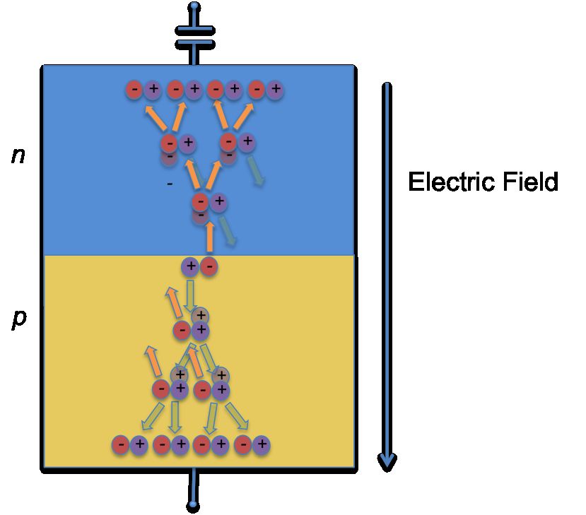
The Geiger Mode in Silicon
When a sufficiently high electric field (> 5 x 10⁵ V/cm) is generated within the depletion region of the silicon, a charge carrier
created in this region will be accelerated to a point where it carries sufficient kinetic energy to create secondary charge pairs
through a process called impact ionization. In this way, a single photoelectron can trigger an self-perpetuating ionization cascade
that will spread throughout the silicon volume subjected to the field. The silicon will break down and become conductive,
effectively amplifying the original photoelectron into a macroscopic current flow. This process is called Geiger discharge, in
analogy to the ionization discharge observed in a Geiger-Müller tube. This process is illustrated in Figure 2.
A photodiode operated in Geiger mode employs this mechanism of breakdown to achieve a high gain. The p-n junction region
is designed in such a way that it can sustain a reverse bias beyond its nominal breakdown voltage, creating the necessary high
field gradients across the junction. Once a current is flowing it should then be stopped or ‘quenched’. Using passive quenching
SensL © 2011 1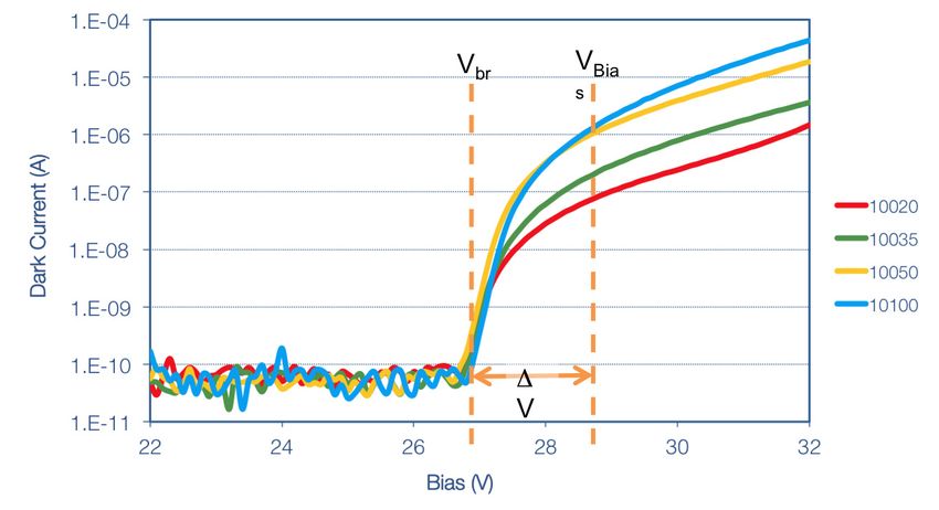
Introduction to the SPM
TECHNICAL NOTE
Figure 2 schematic of the Geiger Figure 3a) Breakdown, quench and reset cycle Figure 3b) “digital” pulse output from a
mode as used in SPM operation of a photodiode working in the Geiger mode. photodiode working in the Geiger mode
(i.e. no active circuitry), this is achieved through the means of a series resistor RQ which limits the current drawn by the diode
during break down, and hence lowers the reverse voltage seen by the diode to a value below its breakdown voltage. This cycle
of breakdown, avalanche, quench and subsequent reset of the bias to a value above the breakdown voltage is illustrated in
Figure 3a.
In this way, a single photodiode device operated in Geiger-mode functions as a photon-triggered switch, in either an ‘on’ or ‘off’
state, and therefore cannot provide proportional information regarding the magnitude of an instantaneous photon flux. A ‘binary’
output such as that in Figure 3b would be the result. Regardless of the number of photons interacting within a diode at the same
time, it will produce a signal of ‘1’ photon.
The Silicon Photomultiplier
To overcome this lack of proportionality, the Silicon Photomultiplier
integrates a dense array of small, electrically and optically isolated Geiger-
mode photodiodes. Each photodiode element in the array is referred to as
a “microcell”. Typically numbering between 100 and 1000 per mm2, each
microcell has its own quenching resistor. The signals of all microcells are then
summed to form the output of the SPM. A simplified electric circuit to illustrate
the concept is shown in Figure 4. Each microcell detects photons identically
and independently. The sum of the discharge currents from each of these
individual binary detectors combines to form a quasi-anlog output, and is thus
capable of giving information on the magnitude of an incident photon flux. The
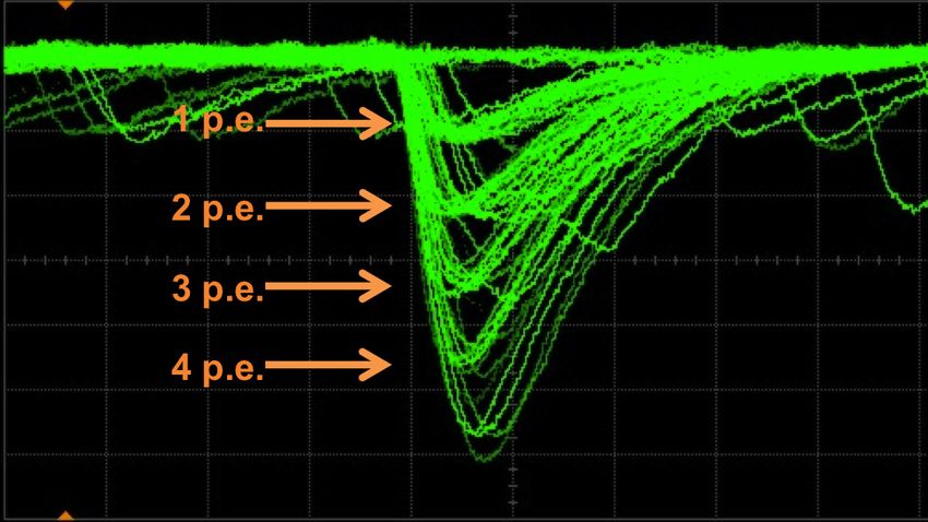
response to low-level light pulses is shown in Figure 5, and a spectrum of the Figure 4 An array of microcells (photodiode
same pulse is shown in Figure 6. plus quench resistor) with summed output
Figure 5 Oscilloscope shot showing the discrete Figure 6 Photoelectron spectrum of the
nature of the SPM output when illuminated by SPM, achieved using brief, low-level light
brief pulses of low-level light. pulses
SensL © 2011 2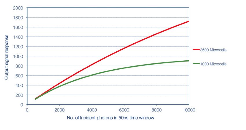
Introduction to the SPM
TECHNICAL NOTE

Silicon Photomultiplier Performance Parameters

The users of SPM detectors will typically be interested in the following parameters: gain, PDE, noise, dynamic range, timing and
temperature sensitivity. The following sections define these parameters, as well as giving some of the theory behind the parameter
and also some typical values.

Over-Voltage

The breakdown voltage (Vbr) is the bias point at which the electric
field strength generated in the depletion region is sufficient to create
a Geiger discharge. The point of breakdown is clearly seen on an I-V
plot by the sudden increase in current, as in Figure 7. For optimized
performance, SensL recommend a working bias voltage (Vbias) of 2V
above the breakdown voltage for their devices. This 2V is referred
to as the ‘over-voltage’ (DV) and is critical in defining the important
performance parameters of the SPM.
                                                                            Figure 7 Dark current as a function of voltage for 1mm SPMs
Gain                                                                           of various microcell size (20um, 35um, 50um, 100um).

                                                         Each microcell in an SPM is comprised of a Geiger-mode photodiode
                                                         in series with an integrated quench resistor. Each microcell generates a
                                                         highly uniform and quantized amount of charge every time the microcell
                                                         undergoes a Geiger breakdown. The gain of a microcell (and hence the
                                                         detector) is defined as the ratio of the output charge to the charge on an
                                                         electron. The output charge can be calculated from the over-voltage and
                                                         the microcell capacitance.

                                                              C ⋅ ΔV
                                                                                               G=
    Figure 8 Gain as a function of over-voltage for      					 q
 different microcell size SPMs (20um, 35um, 50um,
                         100um)                      Due to the unique way in which the SPM operates, each detected photon
                                                     results in a highly quantized output pulse, as was shown in Figures 5. If
                                                     such pulses are integrated by an ADC and a spectrum is formed, the peaks
due to successive numbers of detected photons will be clearly visible. Such a spectrum is shown in Figure 6. The separation
between each pair of adjacent peaks (in pC) is constant and corresponds to the charge from a single Geiger discharge. This
can therefore be used to accurately calculate the gain, using the equation above. By repeating this procedure at different over-
voltage values, a plot such as that in Figure 8 can be formed.

Photon Detection Efficiency

                                                               The photon detection efficiency (PDE) of an SPM is the statistical
                                                               probability that an incident photon will produce a Geiger pulse from
                                                               one of the SPM microcells. It differs slightly from the quantum
                                                               efficiency (QE) that is quoted for a PMT or APD, due to the microcell
                                                               structure of the device. The PDE is a function of wavelength and bias
                                                               and is given by

                                                                                    PDE(λ,V ) = η (λ )⋅ ε (V )⋅ F

 Figure 9 Responsivity as a function of wavelength for
           SPMs of different microcell size                    where h(l) is the quantum efficiency of silicon, e(V) is the avalanche
            (20um, 35um, 50um, 100um)                          initiation probability and F is the fill factor of the device. The avalanche

                                                               SensL © 2011                                                              3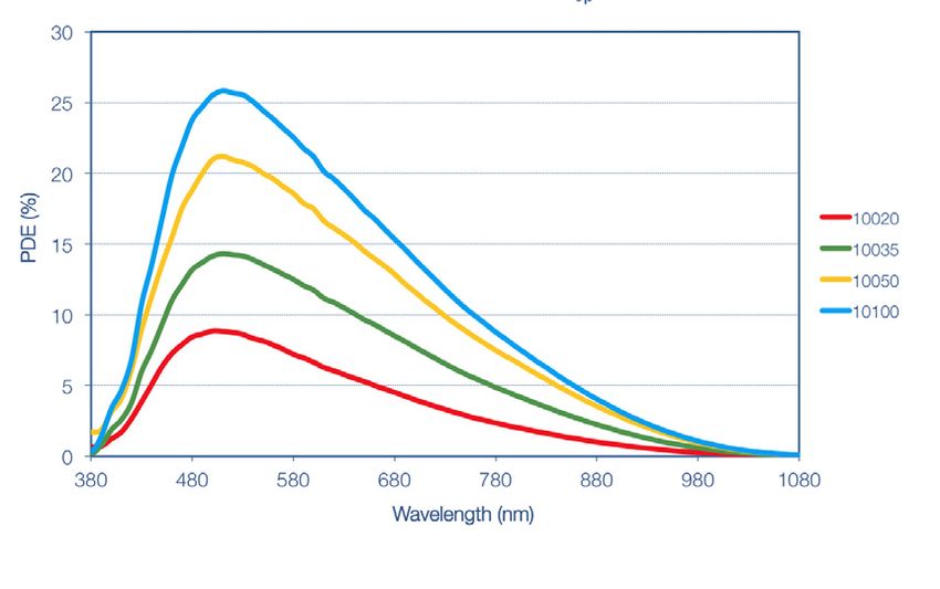
Introduction to the SPM
TECHNICAL NOTE

initiation probability takes into account the fact that not all generated photoelectrons will go on to initiate an avalanche. The fill
factor is the ratio of active to inactive area on the SPM, as a result of the gaps between the microcells.

The PDE is commonly calculated from the responsivity of the detector which is defined as the average photocurrent produced
per unit optical power and is given by

                                         Ip
                                    R=
                                         Pop

where Ip is the measured photocurrent and Pop is the incident optical power
at a particular wavelength over the detector area. The responsivity is typically
expressed in units of Amps per Watt (A/W). A plot of the measured SPM
responsivity is shown in Figure 9. The PDE can then be determined from the
responsivity from the relation

                                               R h⋅c
                                    PDE =       ⋅                                  Figure 10 PDE as a function of wavelength for different
				                                           G λ ⋅e                                    microcell sizes (20um, 35um, 50um, 100um)

where G is the gain of the SPM microcells, h is the Planck constant, c is the speed of light, l is the wavelength of the incident
light and e is the electronic charge. In this method the gain of the SPM microcells should be accurately known and the SPM
should be operated in its linear region. It should be noted that this method does not account for the contributions of cross-talk
or after pulsing and therefore gives a slight over-estimation of the PDE. A plot of the PDE for SPMs with different microcell sizes
is shown in Figure 10.

Noise

                                                                  Noise is a general term that may cover all sources of unwanted
                                                                  signal in the system and is superimposed onto the measured
                                                                  signal. The noise ultimately imposes a limit on the smallest signal
                                                                  that can be measured.

                                                                  The main source of noise in an SPM is the dark count rate
                                                                  (DCR), which is primarily due to thermally generated electrons
                                                                  that go on to create an avalanche in the high field region. The
                                                                  signals resulting from the breakdown of the cell, due to either
                                                                  photoelectrons or thermally generated electrons, are identical.
                                                                  Therefore, these electrons form a source of noise at the single
                                                                  photon level. If a threshold can be set above the single photon
  Figure 11 Dark count rate as a function of over-voltage for     level, false triggers from the noise can be avoided, but the dark
 1mm SPMs of two different microcell sizes (20um and 35um)        counts will always form a contribution to the measured signal.

                                                            Since this noise is comprised of a series of pulses, its magnitude
                                                            is often quoted as a pulse rate, typically in kHz or MHz. For
continuous or current integration measurements, it might be more convenient to consider the contribution as a ‘dark current’
in μA.

It should be noted that the magnitude of the DCR itself is not the noise contribution. If a given source of noise was always constant,
then it could easily be subtracted from the signal. It is instead the fluctuations on the noise which degrade a measurement. The
occurrence of the dark pulses is Poissonian in time and so the noise contribution can be taken as the square root of the DCR.

The DCR can be measured with a simple counting system, setting a threshold set at the 0.5p.e. level. The plots in Figure 11
show the noise as a function of over-voltage. In addition to the bias, the DCR is also a function of temperature, microcell size
and overall detector area.

                                                                SensL © 2011                                                            4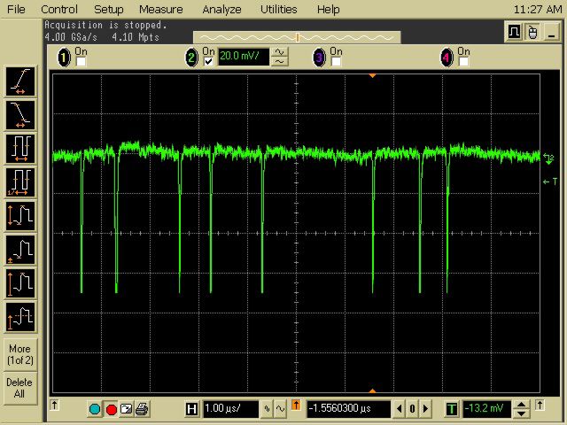
Introduction to the SPM
TECHNICAL NOTE
Optical Crosstalk
An additional component of SPM noise is that of optical cross-talk between microcells.
When undergoing avalanche, carriers near the junction emit photons as they are
accelerated by the high electric field. These photons tend to be in the near infrared
region and can travel substantial distances through the device. Typically 2x10⁵ are
emitted per electron crossing the junction. These photons can travel to neighboring
microcells and may initiate a subsequent Geiger avalanche there. The crosstalk
probability is the probability that an avalanching microcell will initiate an avalanche in a
second microcell. The process happens instantaneously and as a consequence, single
photons may generate signals equivalent to a 2, 3 or higher photoelectron event. This
can be seen for the middle pulse shown in Figure 12 where the pulse height is equivalent
Figure 12 Oscilloscope shot
to a 2-photon event.
showing dark counts
The optical crosstalk
probability is a function of SPM over-voltage and the distance
between neighboring microcells, and can be estimated by the
ratio of the count rate at the second photoelectron level to the
count rate at the single photoelectron level. Figure 13 shows the
result of plotting the DCR as a function of threshold position,
which produces a step-like curve. The flat regions of the curve
correspond to the frequency of dark counts at the single, double,
triple photoelectron level. Crucially, this plot shows that with a
threshold level set to 5 p.e., the dark count trigger rate will be
negligible.
Figure 13 Dark count rate of a 1mm, 35um microcell SPM, as a
function of counting threshold, for different over-voltages.
Dynamic Range and Linearity
The dynamic range of a detector can be defined as the optical signal level range over which the detector provides a useful
output. For an SPM, this range extends from the lowest signal level detectable, to the optical signal level that results in all of the
SPM microcells detecting photons simultaneously (within the microcell dead-time). At this point the output signal completely
saturates since no more microcells are available to detect incoming photons, until some of the microcells have recovered back
to their sensitive (charged) state.
The dynamic range of an SPM is therefore a function of the total number of microcells and the PDE of the device. Since the
PDE of an SPM is a function of the SPM bias voltage and wavelength of the incident photons, the dynamic range of an SPM
is also a function of these parameters. The number of microcells fired as a function of the number of incident photons can be
approximated by the expression,
⎛ ⎛ PDE(V, λ )⋅ N ph ⎞⎞
N fired ( M,V, λ ) = M ⎜⎜1− exp ⎜ − ⎟⎟⎟
⎝ ⎝ M ⎠⎠
where Nfired is the number of microcell fired, Nph is the number of incident
photons, M is the number of SPM microcells and PDE is the SPM photon
detection efficiency. The expression also assumes that the incoming
photons are evenly distributed across the surface of the SPM. Above a
certain signal level, and before saturation, the SPM response becomes
Figure 14 Linearity for SPMs with either 3600 or 1000 sub-linear. This is because the output pulse of a single microcell is
microcells independent of the number of incident photons that initiated the output
pulse. As the number of incident photons per microcell per second
SensL © 2011 5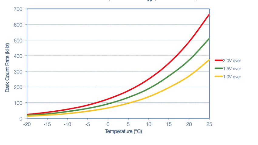
Introduction to the SPM
TECHNICAL NOTE

increases, the probability increases that two or more photons will interact in the same microcell at the same time. The SPM
output begins to saturate when the number of detected photons begins to approach the number of microcells (M).

                                                          N ph ⋅ PDE → M

In summary, at low optical signal levels the SPM photocurrent is proportional to the incident optical power, giving a linear
detector response. As the optical power increases the SPM photocurrent begins to deviate from linearity due to the limited
number of microcells, and finally saturates. Figure 14 shows a simulation of the response for a 3600 and 1000 microcell SPM
when uniformly illuminated with 50ns duration light pulses of varying brightness.

Pulse Shape

A typical single photoelectron pulse for a 3mm, 35mm microcell SPM is
shown in Figure 15. The rise time of the SPM is dependent upon the total
area of device, and specifically, the capacitance resulting from the tracks
that connect all of the microcells. The rise time varies from ~1ns for a 1mm
device to ~10ns for a 6mm device.

The recovery time, or decay time of the pulse, is irrespective of the detector
size, but is instead determined by the microcell reset period, given by
                                                                                    Figure 15 Typical pulse from a 3mm, 35um microcell
                                   treset = RQ·C                                                            SPM

where C is the effective capacitance of the microcell and RQ the value of the quench resistor. Since the capacitance of the
microcell will depend upon its area, the reset time will vary for different microcell sizes, with a 100mm SPM having a signigicantly
longer reset time than a 20mm SPM.

Temperature Dependency

The primary effects of temperature on the SPM are a change in the breakdown
voltage of the diode and in the dark count rate.

The breakdown voltage changes as a function of temperature, as shown in Figure
16, and unless compensated for, this will result in a change in the effective over-
voltage. Since the over-voltage affects many of the SPM’s characteristics, it
follows that for stable operation the detector should have its temperature
regulated. Since the SPMs thermal mass is very small (the detector is only 500mm
thick) it is a simple matter to cool or regulate the temperature with a Peltier device.     Figure 16 Breakdown voltage as a function
If this is not possible, the bias voltage should be adjusted in order to maintain a                      of temperature
constant over-voltage with respect to the altered breakdown voltage.

                                                      If a constant over-voltage is maintained, many parameters, such as gain,
                                                      PDE and timing, will remain the same as at room temperature. However,
                                                      regardless of constant over-voltage, the DCR will be altered by a change in
                                                      temperature, as shown in Figure 17.

                                                      An increase in temperature will increase dark rate, and the converse is
                                                      also true: for every 10oC reduction in device temperature, there is a 50%
                                                      decrease in the dark count rate. Thus, an SPM detector that is cooled with
                                                      thermoelectric (Peltier) coolers, such as the MiniSL, opens up a range of new,
                                                      low-light level applications that require very low noise detectors.
   Figure 17 Dark count rate as a function of
temperature and over-voltage, for a 1mm, 35um
               microcell SPM

                                                               SensL © 2011                                                          6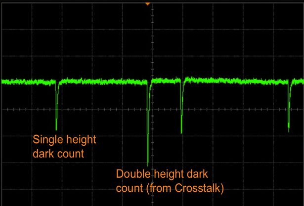
Introduction to the SPM
TECHNICAL NOTE

Comparison with Other Detector Technologies

                                  Low-light photon detectors constitute the enabling technology for a diverse and rapidly growing
                                  range of applications: Nuclear medical imaging, radiation detection, fluorescence analysis,
                                  spectroscopy, quality control or meteorology all require detectors that serve to quantify and/or
                                  time stamp light signals with anywhere from 1 to ~1000 photons per event. The ideal detector
                                  provides a response proportional to the incident photon flux and incorporates an internal gain
                                  mechanism, yielding signals of sufficient magnitude to be easily processed. It should offer sub-
                                  nanosecond response times and broad spectral sensitivity, be robust, easy to operate and
     Figure 18 A typical PMT      only generate manageable amounts of noise or dark count rates.

To date the Photomultiplier tube (PMT), a well established and widely available vacuum tube device, has been the detector of
choice for such applications. The semi-transparent photocathode deposited inside the entrance window inherently limits the
PDE they can achieve, with typical PMTs having about 20% at 420nm. A gain of 1-10e6 is achieved at the cost of a high bias
voltage of 1-2kV, which requires the use of costly high-voltage power supplies. PMTs are generally stable and low noise but are
bulky and delicate due to their vacuum tube structure. They can also be adversely affected by magnetic fields which will limit
their suitability for some applications.

Solid state devices have many practical advantages over the PMT, and this led to the PIN diode
being used in applications where PMTs were too bulky or delicate, or where high voltages were
not possible. However, PIN diodes are severely limited by their complete lack of internal gain.
The Avalanche Photodiode (APD) is a more recent technology, an extension of the simple PIN
diode. Here the reverse bias is raised to a point where impact ionization allows for some internal
multiplication, but is below the breakdown bias where the Geiger mode would take over. In this
way, a gain of around a 100 is achieved for a bias of 100-200V. With special manufacture, it is
possible for gains of several thousand to be reached using an HV bias of >1500V. Whilst the gain Figure 19 APD detectors
may be lower than that of a PMT, APDs have the advantage of a PDE which can be >65% and
also a compact size, ruggedness and insensitivity to magnetic fields. Their main drawbacks are
their excess noise (associated with the stochastic APD multiplication process) and in an important trade-off: The capacitance
increases with increasing device area and decreasing thickness, whereas the transit times of the charge carriers increase with
increasing thickness, implying a performance trade-off between noise and timing. They are limited in size to ~10mm diameter.

The SPM has high gain and moderate PDE (~20%), very similar to the PMT, but has the physical benefits of compactness,
ruggedness and magnetic insensitivity in common with the PIN and APD. In addition, the SPM achieves its high gain (1e6) with
very low bias voltages (~30V) and the noise is almost entirely at the single photon level. Because of the high degree of uniformity
between the microcells the SPM is capable of discriminating the precise number of photoelectrons detected as distinct, discrete
levels at the output node. The ability to measure a well resolved photoelectron spectrum is a feature of the SPM which is
generally not possible with PMTs due to the variability in the gain, or excess noise. Despite the fact that the SPM is sensitive to
single photons, its dark count rate of ~100kHz/mm2 at room temperature renders it unsuitable for use for applications at very
low light levels. However, with the application of cooling (such as with the SensL MiniSL) a two order of magnitude reduction in
the dark count rate is readily achievable. Further technical details on SensL’s full range of SPMs can be found at

www.sensl.com/documentation.

                                                            SensL © 2011                                                         7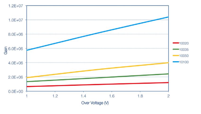
Introduction to the SPM
    TECHNICAL NOTE

                                                    PIN                    APD                    PMT               SPM
                 Gain                                 1                     10 2
                                                                                                    10 6
                                                                                                                      106
                 Operational Bias                   Low                     High                   High             Low**
                 Temp. Sensitivity                  Low                     High                   Low               Low
                 Mechanical
                                                    High                  Medium                   Low               High
                 Robustness
                 Ambient light
                                                     OK                     OK                      NO                OK
                 exposure?
                 Spectral range                     Red                     Red                  Blue/UV            Green
                 Readout / Electronics           Complex                 Complex                  Simple            Simple
                 Form factor                     Compact                 Compact                   Bulky          Compact
                 Large area available?               No                      No                     Yes               Yes
                 Sensitive to magnetic
                                                    Yes*                    Yes*                    Yes               No
                 fields?
                 Noise                              Low                   Medium                   Low               High
                 Rise time                        Medium                   Slow                    Fast              Fast

                   * Due to the requirement for the external electronics to be located close to the detector
                   ** SPM from SensL, having an operational bias of 30V, meet the requirements of the Extra Low Voltage directive

                                                                                                                                www.sensl.com
                                                                                                                               sales@sensl.com
                                                                                                                 +353 21 240 7110 (International)
                                                                                                                +1 650 641 3278 (North America)
                                                   All specifications are subject to change without notice

Rev. 3.1, October 2011                                               SensL © 2011                                                              8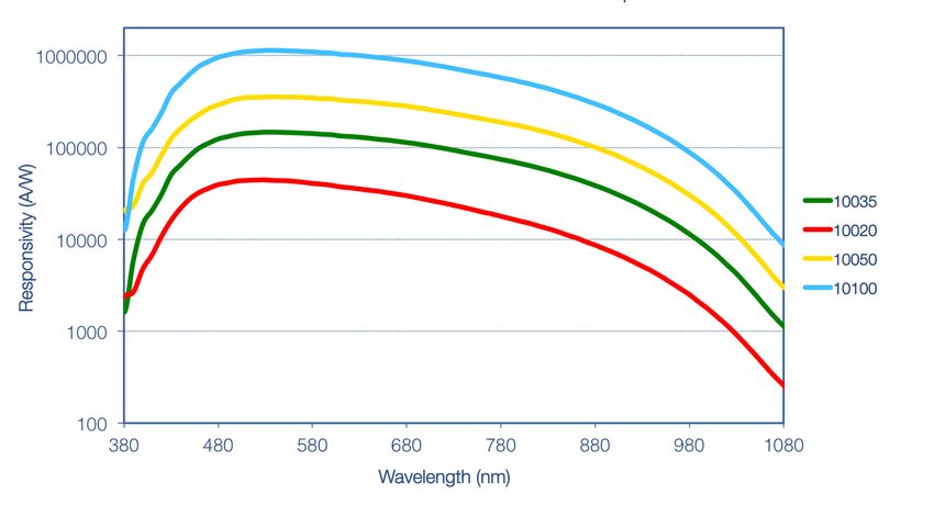
You can also read