Arrays of individually controllable optical tweezers based on 3D-printed microlens arrays
←
→
Page content transcription
If your browser does not render page correctly, please read the page content below
Research Article                                     Vol. 28, No. 6 / 16 March 2020 / Optics Express   8640

Arrays of individually controllable optical
tweezers based on 3D-printed microlens arrays
D OMINIK S CHÄFFNER , 1,* T ILMAN P REUSCHOFF , 1 S IMON
R ISTOK , 2 L UKAS B ROZIO, 1 M ALTE S CHLOSSER , 1 H ARALD
G IESSEN , 2 AND G ERHARD B IRKL 1
1 Institut
         für Angewandte Physik, Technische Universität Darmstadt, Schlossgartenstraße 7, 64289
Darmstadt, Germany
2 4. Physikalisches Institut, Universität Stuttgart, Pfaffenwaldring 57, 70569 Stuttgart, Germany
* dominik.schaeffner@physik.tu-darmstadt.de

www.iap.tu-darmstadt.de/apq

Abstract: We present a novel platform of optical tweezers which combines rapid prototyping
of user-definable microlens arrays with spatial light modulation (SLM) for dynamical control
of each associated tweezer spot. Applying femtosecond direct laser writing, we manufacture a
microlens array of 97 lenslets exhibiting quadratic and hexagonal packing and a transition region
between the two. We use a digital micromirror device (DMD) to adapt the light field illuminating
the individual lenslets and present a detailed characterization of the full optical system. In an
unprecedented fashion, this novel platform combines the stability given by prefabricated solid
optical elements, fast reengineering by rapid optical prototyping, DMD-based real-time control
of each focal spot, and extensive scalability of the tweezer pattern. The accessible tweezer
properties are adaptable within a wide range of parameters in a straightforward way.

© 2020 Optical Society of America under the terms of the OSA Open Access Publishing Agreement

1.    Introduction
With his seminal publications on optical tweezers in the 1970s [1,2], A. Ashkin has put forth a
technique which nowadays is widely used in many different research fields, including physics,
chemistry, biology, and medical research [2–5]. Granting a high level of dynamic range in the
interaction strength between light and matter, optical tweezers are extremely versatile and can be
used in order to monitor and control the external degrees of freedom of a large variety of target
objects ranging from single atoms to living organisms. Surpassing the original configuration
of using one single laser spot, means of acousto-optical deflection (AOD) [6,7], spatial light
modulation (SLM) [6,8–13], or implementations based on microlens arrays (MLA) [14,15]
facilitate multi-site tweezer systems with complex and parallelized means of manipulation. The
MLA approach, in specific, offers unprecedented scalability due to the lithographic production
process. This allows for the creation of many thousands of diffraction-limited tweezer sites
[14,15], not limited by the finite frequency spectrum of AODs or the resolution-versus-size
constraints of liquid-crystal-based SLMs. However, a modification of the tweezer pattern requires
a new fabrication of the employed MLA with large investments for the lithographic masks. This
causes long turnaround times and reduces flexibility.
   In this work, we report on the realization of a novel platform of optical tweezers that overcomes
previous limitations by combining two powerful state-of-the-art technologies: rapid prototyping
of microlens arrays based on direct laser writing and in-situ access and dynamic control of each
tweezer spot based on digital micromirror device (DMD) spatial light modulation. We achieve
an efficiency between the values reported for holographic DMD tweezer generation [16] and
liquid-crystal (LC) based phase modulating SLMs [12], but our DMD-based approach offers
at least an order of magnitude higher addressing rates as compared to LC-based configurations
[12,16]. In this way, we significantly extend the state-of-the-art of optical tweezers by combining

#386243                                                                     https://doi.org/10.1364/OE.386243
Journal © 2020        Received 18 Dec 2019; revised 17 Jan 2020; accepted 17 Jan 2020; published 10 Mar 2020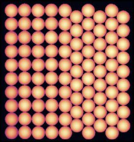
Research Article                                    Vol. 28, No. 6 / 16 March 2020 / Optics Express   8641

the high-quality foci typical for microlens setups with kilohertz rates for addressability in versatile
yet stable configurations. We present in detail design and manufacturing of the MLA, the optical
setup combining the MLA with the DMD-based control of each individual tweezer, and the
characterization of the full optical setup. This novel experimental platform finds immediate
application in the investigation and manipulation of biological systems, dielectric particles,
large atomic ensembles, as well as individual neutral atoms. For a detailed discussion, we have
adapted the system to single-atom quantum simulation as demonstrated in [14,15,17] with design
parameters optimized for a setup similar to the one detailed in [15].

2.   Design and manufacturing of microlens arrays with versatile geometries
Three-dimensional printing by femtosecond direct laser writing of microfabricated optics has
become a well established technology in recent years [18–20] providing tremendous accuracy and
short design and production cycles. We apply this technique to the production of a custom-design
MLA consisting of circular shaped spherical lenslets. Figure 1 presents the layout (a) of the
microlens array together with the results of the post-fabrication characterization measurements
(b-d). Maintaining a lens pitch and diameter of 110 µm, the array features sections with
quadratic and hexagonal packing, respectively, including a region of transition from rectangular
to hexagonal symmetry. We use 3D dip-in direct laser writing [18,19] with a femtosecond
lithography system (Nanoscribe Photonic Professional GT) to sequentially imprint 97 spherical
microlenses on a fused silica substrate with a thickness of 700 µm. As printing can be executed
with a writing speed of about 10 lenslets per hour this manufacturing approach is especially
suited for rapid prototyping of systems with up to about 100 lenslets. If required, processing
speed can be significantly increased by parallelized writing techniques [20].

       Fig. 1. Layout and characterization of the manufactured microlens array. (a) The array
       is designed to consist of 97 lenslets with a fundamental pitch of 110 µm in quadratic and
       hexagonal packing including a region of transition from rectangular to hexagonal symmetry.
       (b) Inspection of the manufactured array by white-light microscopy confirms the successful
       manufacturing process. (c) A confocal microscope is used to analyze the surface of the
       microlens array. (d) Profile of one of the microlenses and fit for the determination of the
       quality of the spherical surface and the radius of curvature R. The inset provides a more
       detailed view on the central region of the lenslet.
Research Article                                 Vol. 28, No. 6 / 16 March 2020 / Optics Express   8642

   A typical height of the curved lens profile measures only a few microns. Hence keeping the
surface roughness at a minimum plays an important role. We use the photoresist Nanoscribe
IP-S (index of refraction n = 1.505 at a wavelength of 796 nm [21]) which has been specifically
developed for this purpose. The printing resolution of the lithography system normal to the
substrate surface is 100 nm. As a first step of verifying a successful fabrication process, we
inspect the printed lens array with a standard optical microscope (Nikon Eclipse LV100) and
retrieve the white light image shown in Fig. 1(b). Using a commercial confocal microscope
setup (NanoFocus µ surf expert), we obtain a detailed view of the microlens surfaces (Fig. 1(c)).
From a typical lens profile (Fig. 1(d)) we extract a radius of curvature of R = 580(2) µm of the
spherical surface with an rms-deviation of 0.03 µm from a perfect sphere within 90 % of the lens
diameter (i.e. 99 µm). This results in an effective numerical aperture of NA = 0.045(2). The
inset in Fig. 1(d) provides an enlarged view of the profile. The surface irregularities match the
100 nm resolution of the lithography system normal to the substrate surface. As a next step, we
analyze the focal plane of the microlens array when illuminated by a laser beam at a wavelength of
λ = 796.7 nm and a diameter much larger than a microlens diameter. Approximating the resulting
foci with two-dimensional Gaussian intensity distributions yields a 1 e2 -waist of wq = 6.5(3) µm

in the quadratic and wh = 6.4(3) µm in the hexagonal region, respectively. These values are in
excellent agreement with simulated wavefront propagation using the lenslet design parameters
and the measured radius of curvature leading to diffraction limited performance of the tweezer
array as detailed in Sec. 3.

3.   Tweezer array with extended light field control using a spatial light modulator
The schematic setup of our novel tweezer platform is visualized in Fig. 2(a). We employ a
DMD (Texas Instruments Lightcrafter EVM) in order to render the microlenses selectively
addressable and to dynamically modify the light field that illuminates every single lenslet of the
MLA during operation of the tweezer array. The micromirror array with a size of 6.57 mm x
3.70 mm features 608 x 684 quadratic mirrors with a pitch of 7.64 µm along the mirror edges
whose tilt angle relative to the DMD surface can be individually set to two distinct orientations of
±12◦ , respectively, with an update rate of up to 4 kHz. For our application [15], a Gaussian laser
beam at a wavelength of λ = 796.7 nm and a 1 e2 -radius of wB = 1.2 mm illuminates the DMD

under an incident angle of α ≈ 26◦ leading to deflection of the third diffraction order normal
to the DMD surface and along the optical axis of the subsequent optical setup. A spatial filter
blocks all unwanted diffraction orders. We obtain a typical efficiency of the DMD section of
our setup of η = 33 % which is limited by the fact that α deviates from the angle of specular
reflection off a single mirror of +24°, by light being diffracted into other diffraction orders, by
finite mirror and window efficiencies, and a limited filling factor as detailed in the datasheet.
   Using a confocal telescope of two achromatic doublets L1 and L2 with focal lengths of
f1 = 100 mm and f2 = 45 mm, respectively, the DMD plane is mapped onto the microlens array
with every lenslet illuminated by a circular pattern of mirrors as schematically illustrated in
Fig. 2(b). Due to the fact that the pitch of the microlens array (110 µm) is not a multiple of
the demagnified micromirror pitch (7.64 µm · f 2 /f 1 = 3.44 µm) the numbers of mirrors that are
assigned to different lenslets are not identical, yet typically 730(8). This results in an effective
microlens illumination diameter of 109(1) µm. As exemplified in Fig. 2(c), irradiation of each
microlens, and consequently each focal spot, can be individually turned on (off) by tilting the
respective mirrors into the +12° (−12°) orientation, respectively. Sections of the MLA not
corresponding to a lenslet are not illuminated. Thus, stray light resulting from areas outside the
lenslets is avoided. In regions with quadratic (hexagonal) packing, 71 % (82 %) of the DMD
mirrors contribute to the tweezer light field.
   The focal plane of the microlens array is demagnified (magnification M34 = f4 /f3 = 0.094(3))
using an achromatic doublet L3 with a focal length of f3 = 400 mm in combination with a
Research Article Vol. 28, No. 6 / 16 March 2020 / Optics Express 8643
Fig. 2. Novel tweezer platform including DMD-based microlens addressing, mapping
optics, and relay optics for demagnification. (a) The incident laser beam illuminates the
surface of the DMD under an incident angle of α ≈ 26◦ resulting in the third diffraction
order to be deflected orthogonally off the DMD surface. Two lenses L1 and L2 map the
DMD surface onto the microlens array whose focal plane is demagnified onto the tweezer
plane by the relay optics with lens L3 and microscope objective L4. As shown schematically
in (b) switching mirrors within circular regions on the DMD can be used to (c) address
individual and groups of microlenses and (d) switch the corresponding tweezer foci.
microscope objective L4 with an effective focal length of f4 = 37.5(10) mm yielding a tweezer
array with a measured spot separation of d = 10.2(3) µm. Figure 2(d) shows an image of the
tweezer plane taken with a CCD camera after applying the illumination pattern depicted in Fig.
2(c). In this straightforward fashion, the setup grants access to versatile trap geometries of the
tweezer array (Fig. 3) consisting of well defined foci with measured waists of wq = 1.36(5)
µm in the quadratic and wh = 1.29(6) µm in the hexagonal region which are diffraction limited
by the numerical aperture of the microscope objective L4 (NA = 0.25(2)). While in Fig. 3(a,
left) an image of the fully activated array of 97 tweezers is shown, several tweezer spots are
turned off in Fig. 3(b, left), in order to generate a modified periodic pattern. The accessible
tweezer geometries range from the full array to selected sections of pure quadratic or hexagonal
symmetry, to the implementation of single-site defects through deactivation of single spots (Fig.
3(c)), and to freely definable symmetries (Fig. 3(d)). The cross sections (Fig. 3(a, right) and
Fig. 3(b, right)) confirm the high quality of the tweezer pattern and the high contrast at which
individual tweezers can be switched. The Gaussian envelope extracted from a fit to the cross
section in Fig. 3(a, right) is consistent with the shape of the beam incidenting on the DMD. If a
uniform intensity distribution for all tweezers is required [17], either an incident beam with flat
top profile can be used or site-selective intensity optimization via deactivating a subset of the
mirrors corresponding to each lenslet can be applied. Due to the large number of 730(8) mirrors
per lenslet, intensity adjustment can be achieved on a 0.2 % level in the range of 20 % to 100 %
of the full intensity without degrading the quality of the tweezers.
Finally, we want to put these results into perspective with state-of-the-art tweezer arrays used
for our targeted application. As demonstrated in [15], microlens-array-based optical tweezer
setups are routinely used to trap individual neutral atoms in foci with a waist of typically 1.45(10)
µm and a power of about 1 mW facilitating a trap depth on the order of kB · 1 mK. The presented
platform provides these parameters with additional means of flexibility. Furthermore, since theResearch Article Vol. 28, No. 6 / 16 March 2020 / Optics Express 8644
Fig. 3. Characterization of the tweezer array after reimaging: (a) Fully enabled tweezer array
with 97 lenslets (left) and a cross section along the dashed line showing the diffraction-limited
tweezer spots (right). For our application we illuminate the DMD with a Gaussian laser
beam, resulting in a Gaussian envelope of the tweezer intensities. (b,c,d) Selective DMD
addressing of each lenslet enables the creation of versatile tweezer patterns. For a geometry
featuring sets of deactivated spots (b, left) we observe a high extinction ratio between
activated and deactivated spots (b, right). Due to DMD control, single-site defects (c) can be
implemented as well as patterns with modified symmetries (d).
tweezer spot size is ultimately determined by the the NA of L4, the optical setup can be easily
adapted to applications such as confocal or super-resolution microscopy at the limits of current
technology by using a state-of-the-art high-NA microscope objective as L4.
4. Conclusion
We have introduced a novel universal platform for the creation of large-scale tweezer arrays
with single-site addressability based on microlens arrays produced by 3D femtosecond direct
laser writing. We have manufactured an array composed of 97 circular lenslets in quadratic and
hexagonal packing and create a tweezer array with foci having diffraction-limited waists in the
single-micrometer regime and separations of 10.2(3) µm. Through modification of our relay
optics, the tweezer parameters of the reported platform can easily be adapted to other tweezer
implementations with state-of-the-art parameters and added flexibility. As each tweezer is defined
by the corresponding microlens within a solid optical microlens array, the present system exhibits
a high degree of stability and precision, which would typically be at the expense of short-term
reconfigurability. In contrast, our system is perfectly suited for on-demand optimization of the
imprinted optics via rapid prototyping and exhibits additional means of dynamical reconfiguration
owing to the DMD-based spatial control of the incident light. The achieved efficiency for our
DMD-controlled MLA of about 25 % is below the values of 80 % typical for holographic usage of
phase modulating SLMs while exceeding the efficiency of holographic setups relying on DMDs
which is typically at about 10 %. The large number of mirrors assigned to each lenslet also renders
gradual trap depth modulation possible via partial deactivation of mirrors. Moreover, the present
system can be easily extended by an ancillary movable optical tweezer in the manner detailed
in [15,22] for the purpose of transporting objects between traps or equipped with parallelized
position control as demonstrated in [14]. Additionally, our approach is not constrained to twoResearch Article Vol. 28, No. 6 / 16 March 2020 / Optics Express 8645
dimensional arrays: imprinting lenses with a range of different focal lengths makes versatile
three-dimensional geometries accessible in a straightforward way.
Funding
Bundesministerium für Bildung und Forschung (Printoptics); Baden-Württemberg Stiftung
(Opterial); European Research Council (PoC 3DPrintedOptics); Technische Universität Darmstadt
(OA Fund); Deutsche Forschungsgemeinschaft (SPP 1929 GiRyd BI 647/6-2).
Disclosures
The authors declare that there are no conflicts of interest related to this article.
References
1. A. Ashkin, “Acceleration and trapping of particles by radiation pressure,” Phys. Rev. Lett. 24(4), 156–159 (1970).
2. A. Ashkin, Optical Trapping and Manipulation of Neutral Particles Using Lasers (WORLD SCIENTIFIC, 2006).
3. A. Ashkin, “Applications of laser radiation pressure,” Science 210(4474), 1081–1088 (1980).
4. P. Polimeno, A. Magazzù, M. Iatì, F. Patti, R. Saija, C. Degli Esposti Boschi, M. Grazia Donato, P. Gucciardi, P.
Jones, G. Volpe, and O. M. Marago, “Optical tweezers and their applications,” J. Quant. Spectrosc. Radiat. Transfer
218, 131–150 (2018).
5. K. R. Dhakal and V. Lakshminarayanan, “Optical tweezers: Fundamentals and some biophysical applications,” Prog.
Opt. 63, 1–31 (2018).
6. G. Akselrod, W. Timp, U. Mirsaidov, Q. Zhao, C. Li, R. Timp, K. Timp, P. Matsudaira, and G. Timp, “Laser-guided
assembly of heterotypic three-dimensional living cell microarrays,” Biophys. J. 91(9), 3465–3473 (2006).
7. M. Endres, H. Bernien, A. Keesling, H. Levine, E. R. Anschuetz, A. Krajenbrink, C. Senko, V. Vuletic, M. Greiner,
and M. D. Lukin, “Atom-by-atom assembly of defect-free one-dimensional cold atom arrays,” Science 354(6315),
1024–1027 (2016).
8. J. E. Curtis, B. A. Koss, and D. G. Grier, “Dynamic holographic optical tweezers,” Opt. Commun. 207(1-6), 169–175
(2002).
9. S. Bergamini, B. Darquié, M. Jones, L. Jacubowiez, A. Browaeys, and P. Grangier, “Holographic generation of
microtrap arrays for single atoms by use of a programmable phase modulator,” J. Opt. Soc. Am. B 21(11), 1889–1894
(2004).
10. E. Ferrari, V. Emiliani, D. Cojoc, V. Garbin, M. Zahid, C. Durieux, M. Coppey-Moisan, and E. D. Fabrizio,
“Biological samples micro-manipulation by means of optical tweezers,” Microelectron. Eng. 78-79, 575–581 (2005).
11. S. R. Lee, J. K. Kim, Y. J. Won, and K. Oh, “Generation of optical lattice and trapping particle using DMD-ALP,”
in Passive Components and Fiber-based Devices III, vol. 6351 S. B. Lee, Y. Sun, K. Qiu, S. C. Fleming, and I. H.
White, eds., International Society for Optics and Photonics (SPIE, 2006), pp. 587–595.
12. F. Nogrette, H. Labuhn, S. Ravets, D. Barredo, L. Béguin, A. Vernier, T. Lahaye, and A. Browaeys, “Single-atom
trapping in holographic 2D arrays of microtraps with arbitrary geometries,” Phys. Rev. X 4(2), 021034 (2014).
13. D. Stuart and A. Kuhn, “Single-atom trapping and transport in DMD-controlled optical tweezers,” New J. Phys.
20(2), 023013 (2018).
14. M. Schlosser, S. Tichelmann, J. Kruse, and G. Birkl, “Scalable architecture for quantum information processing with
atoms in optical micro-structures,” Quantum Inf. Process. 10(6), 907–924 (2011).
15. D. Ohl de Mello, D. Schäffner, J. Werkmann, T. Preuschoff, L. Kohfahl, M. Schlosser, and G. Birkl, “Defect-free
assembly of 2D clusters of more than 100 single-atom quantum systems,” Phys. Rev. Lett. 122(20), 203601 (2019).
16. N. Holland, D. Stuart, O. Barter, and A. Kuhn, “Efficient and fast algorithms to generate holograms for optical
tweezers,” arXiv preprint arXiv:1711.07845 (2017).
17. M. R. Sturm, M. Schlosser, R. Walser, and G. Birkl, “Quantum simulators by design: Many-body physics in
reconfigurable arrays of tunnel-coupled traps,” Phys. Rev. A 95(6), 063625 (2017).
18. S. Kawata, H.-B. Sun, T. Tanaka, and K. Takada, “Finer features for functional microdevices,” Nature 412(6848),
697–698 (2001).
19. T. Gissibl, S. Thiele, A. Herkommer, and H. Giessen, “Two-photon direct laser writing of ultracompact multi-lens
objectives,” Nat. Photonics 10(8), 554–560 (2016).
20. C. Yuan, K. Kowsari, S. Panjwani, Z. Chen, D. Wang, B. Zhang, C. J.-X. Ng, P. V. y. Alvarado, and Q. Ge, “Ultrafast
three-dimensional printing of optically smooth microlens arrays by oscillation-assisted digital light processing,” ACS
Appl. Mater. Interfaces 11(43), 40662–40668 (2019).
21. M. Schmid, S. Thiele, A. Herkommer, and H. Giessen, “Three-dimensional direct laser written achromatic axicons
and multi-component microlenses,” Opt. Lett. 43(23), 5837–5840 (2018).
22. D. Barredo, V. Lienhard, S. de Léséleuc, T. Lahaye, and A. Browaeys, “Synthetic three-dimensional atomic structures
assembled atom by atom,” Nature 561(7721), 79–82 (2018).You can also read