Seamless multi-reticle photonics - Bowers
←
→
Page content transcription
If your browser does not render page correctly, please read the page content below
2984    Vol. 46, No. 12 / 15 June 2021 / Optics Letters                                                                        Letter

Seamless multi-reticle photonics
Warren Jin,1,2               Avi Feshali,2 Mario Paniccia,2                  AND    John E. Bowers1, *
1
 ECE Department, University of California, Santa Barbara, Santa Barbara, California 93106, USA
2
 Anello Photonics, Santa Clara, California 95054, USA
*Corresponding author: bowers@ece.ucsb.edu

Received 8 April 2021; revised 21 May 2021; accepted 26 May 2021; posted 26 May 2021 (Doc. ID 427289); published 15 June 2021

While Moore’s law predicted shrinking transistors would                   interconnect PICs interfacing with those switches may soon
enable exponential scaling of electronic circuits, the foot-              surpass a single reticle. An 8192 element active OPA spanned an
print of photonic components is limited by the wavelength                 entire reticle [6]. Optical switches [4] and gyroscopes [15] have
of light. Thus, future high-complexity photonic integrated                already reached multiple reticles, while a photonic quantum
circuits (PICs) such as petabit-per-second transceivers,                  computer could achieve quantum supremacy in a system span-
thousand-channel switches, and photonic quantum com-                      ning three reticles [7]. The need for multi-reticle PICs motivates
puters will require more area than a single reticle provides.             us to seek a stitching method optimized for photonics.
In our novel approach, we overlay and widen waveguides in                    Multi-reticle exposures have already been used in electronic
adjacent reticles to stitch a smooth transition between mis-              circuits for large-scale phased-array antennas and image sensors.
aligned exposures. In SiN waveguides, we measure ultralow                 Misalignment of exposures normal to the reticle boundary (x
loss of 0.0004 dB per stitch, and produce a stitched delay                direction in Fig. 1) can lead to a gap between reticles, and is
line 23 m in length. We extend the design to silicon chan-                addressed by overlaying the adjacent reticles by a distance L
nel waveguides, and predict 50-fold lower loss or 50-fold                 larger than the alignment tolerance [Fig. 1(a)]. Lateral misalign-
smaller footprint versus a multimode-waveguide-based                      ment δ (y direction) causes an abrupt step in the sidewall as the
method. Our approach enables large-scale PICs to scale                    waveguide crosses the reticle boundary. Deep-UV stepper align-
seamlessly beyond the single-reticle limit. © 2021 Optical                ment error of tens of nanometers [16] has little impact on all but
Society of America                                                        the narrowest electronic wires, but such sidewall discontinuities
https://doi.org/10.1364/OL.427289                                         lead to appreciable loss in photonic waveguides.
                                                                             We propose enlarging the overlay distance and widening
While major progress in the interconnect bandwidth of pho-                the waveguides as they traverse the stitch length L, which
tonic integrated circuits (PICs) has been driven by increasing            results in a seamless transition [Fig. 1(b)]. To design for align-
modulation rates, further improvement in bandwidth will                   ment tolerance δMAX , the waveguide in each reticle widens
require spatial, spectral, and polarization multiplexing [1,2].           linearly by 2δMAX as it traverses the stitch length, L. The
Indeed, a recent demonstration with 1.6 Tbit/s capacity used              angle of the sidewall with respect to the propagation axis is
16 parallel 100 Gbit/s lanes [3]. As each lane needs a driver,            θ = tan−1 (δMAX /L) ≈ δMAX /L. Our scheme applies to a posi-
modulator, and fan-out for electrical and optical connections,            tive photoresist, in which exposed areas (indicated by hatching)
future higher-capacity optical interconnects will occupy even             are dissolved in developer and etched to form the waveguide. For
larger chip areas. Similarly, switches [4], optical phased arrays         a negative resist, each waveguide should instead be narrowed. In
(OPAs) [5,6], quantum circuits [7], and tensor cores [8] have             the case of perfect alignment [Fig. 1(c)], the waveguide widens
all demonstrated optical systems with component counts from               and then narrows in the stitch region. For misalignment half of
several hundreds to tens of thousands, and will grow in area as           the alignment tolerance [Fig. 1(d)], the waveguide widens at the
their capabilities improve. The need for large chips is especially        beginning of the stitch region and narrows at the end, as in the
acute for ultralow-loss photonic platforms [9,10], which are              previous case. However, the width of the waveguide in the center
desirable for microwave photonics [11,12], nonlinear optics [9],          of the stitch is constant, with propagation direction tilted from
and gyroscopes [13–15]. These platforms may have bend radii               the input and output waveguides by the angle θ. For misalign-
of 1 mm or larger [9], and often require PICs at the centimeter           ment equal to the alignment tolerance [Fig. 1(e)], the waveguide
scale.                                                                    width is constant throughout the stitch region, and angles by
   The availability of 300 mm substrates in silicon foundries             θ with respect to the input and output waveguides. Thus, the
and the relatively large dimensions of PIC components enable              lateral misalignment is accommodated by a corresponding
PICs to be fabricated at low cost and high volume using prior-            length of the waveguide with offset angle θ. The widening of the
generation process nodes. Thus, increasing the area of PICs to            waveguide should be adiabatic enough that mode conversion
the size of a reticle and beyond is an economical way to continue         loss is negligible, so the loss of the stitch can be entirely attrib-
to scale performance. In Table 1, we estimate performance as              uted to the junctions at either end of the angled waveguide,
die size grows to multiple reticles. With switch bandwidths               where the propagation direction changes and the phase fronts
projected to reach 51.2 Tbit/s by 2024 [2], the footprint of              of the waveguide modes are misaligned. Accordingly, we refer to

0146-9592/21/122984-04 Journal © 2021 Optical Society of America
Letter                                                                                       Vol. 46, No. 12 / 15 June 2021 / Optics Letters        2985

                                                                                            a
Table 1.      Multi-Reticle Performance of Integrated Optical Systems
                                                                                                 # of Reticles
                                                               1                                    2×2                                     4×4
Interconnect bandwidth (Tbit/s)                               40                                    160                                     640
Optical switch (2D) radix                                 180 × 180                              360 × 360                               720 × 720
Optical neural network size (neurons)                         470                                   1900                                    7500
Quantum circuit mode count (qubits)                           21                                     43                                      86
OPA (2D, passive) emitters                                5,000,000                              20,000,000                              80,000,000
OPA (1D, active) emitters                                    5000                                  20,000                                  80,000
Delay line length (m)                                          6                                     25                                      100
Gyroscope scale factor ((◦ /h)/µrad)                          180                                    23                                      2.8
   a
    We assume single-reticle size 2 cm × 2 cm. Interconnect bandwidth based on bandwidth density 100 Gbit/(s mm2 ) [3]. Switch radix based on 110 µm × 110 µm
unit cell [4]. Neural network, quantum circuit size based on density of 2450 phase tuners per 21 cm2 [7]. Passive 2D OPA size based on 4096 emitters per 576 µm ×
576 µm [5]. Active 1D OPA emitter density based on an 8192 emitter chip [6]. Delay line length, gyroscope scale factor (rotation rate per Sagnac phase) based on
Archimedes spiral of 50 µm pitch, 1 mm minimum bend radius [13].

the stitched waveguide in Fig. 1(a) as an “abrupt” stitch, and our                  δMAX of 300 nm, so that the waveguide widens to a width of
optimized design in Fig. 1(b) as an “angled” stitch consisting of                   3.4 µm at the edge of the reticle. When exposed, adjacent ret-
two “angled” junctions.                                                             icles are overlaid by 500 µm. We design structures with stitch
   We validate our design using 100 nm thick silicon nitride                        lengths L of 20, 100, and 450 µm. We observe a lateral mis-
waveguides in a CMOS-foundry ultralow-loss photonic plat-                           alignment below 20 nm on the fabricated wafer [Fig. 2(b)], so
form [9]. Prior work in a similar platform [14,15] for which                        we use mask bias to apply additional misalignment (y direction)
0.1 dB/m loss is achievable [10] demonstrated abrupt stitching                      of −100, 0, and 100 nm for each stitch length. We fabricate a
junctions with an estimated loss of 0.006 dB/stitch, contrib-                       stitched racetrack resonator for each configuration [Fig. 2(c)].
uting around 0.2 dB/m to the total loss in a 3 m delay line. We                     The resonator transmission spectra were measured and fitted
demonstrate our improved stitching method by fabricating                            to determine the resonator round-trip loss, and compared to a
stitched delay lines 23 m in length with an order-of-magnitude                      control device from the same die, consisting of a non-stitched
lower stitching loss [Fig. 2(a)]. In our design, the input to the                   resonator of identical dimensions. Any excess round-trip loss
stitch is a single-mode waveguide of 2.8 µm width. We select                        of the stitched devices versus the control device was attributed
                                                                                    to the stitch design. The control device features an intrinsic
                                                                                    Q factor of 45 M and round-trip loss of 0.005 dB at 1550 nm
                                                                                    wavelength, allowing us to measure very low stitching losses.
                                                                                    The measured data are presented in Fig. 2(e). For 20, 100, and
                                                                                    450 µm stitch lengths, the mean stitching losses, averaged over
                                                                                    ±100 nm bias and spectral range 1510–1600 nm, are 0.0167,
                                                                                    0.0014, and 0.00041 dB, with standard deviations of the means
                                                                                    0.0003, 0.00008, and 0.00004 dB, respectively. The measured
                                                                                    loss of 0.0004 dB/stitch represents an order-of-magnitude
                                                                                    improvement compared to prior work [4,15].
                                                                                       We compare our measured results with simulation. Rather
                                                                                    than simulate the full structure, we observe that for short stitch
                                                                                    lengths, we expect input and output waveguide modes to couple
                                                                                    directly through the near field such that the loss approaches that
                                                                                    of an abrupt junction, which we simulate by the modal overlap
                                                                                    of the input and output waveguides with 100 nm alignment
                                                                                    error. For large stitch lengths, the stitch is modeled by two
                                                                                    junctions of waveguides with propagation directions differing
                                                                                    by θ, which we calculate by finite-difference-time-domain
Fig. 1. Optimized stitching method. (a) Plan-view of un-optimized                   simulation. The waveguide width of the stitch at the angle
stitched waveguide between adjacent reticles. Black (red) hatched areas
                                                                                    junction tapers up to δMAX wider than the input waveguide
indicate regions exposed by the left (right) reticle; the waveguide is
                                                                                    (W) depending on the misalignment, but δMAX ≪ W, so the
defined by the remaining unexposed areas; the dashed lines indicate the
centers of the respective waveguides; δ indicates the lateral alignment
                                                                                    dependence of loss on misalignment is small. The waveguide
error. Stitching causes abrupt steps in the sidewall at the reticle bound-          width at the junction is simulated as W + δMAX , which provides
ary. (b) Instead, widening the overlaid waveguides over a larger distance           a tight upper bound on the loss. The results of these two models
L results in a continuous sidewall; the angle of the sidewall to the                are plotted with the measured stitching loss [Fig. 2(f )]. The loss
propagation axis is given by θ ; the waveguides widen by 2δMAX yielding             of the 20 µm device agrees with the abrupt junction model,
alignment tolerance δMAX ; regions with both black and red hatching                 whereas the losses of the 100 and 450 µm devices agree with
are exposed by both reticles. The stitched waveguide’s plan-view profile            the angled junction model. Indeed, this suggests for a given
varies from (c) zero misalignment to (d) intermediate misalignment to               misalignment (in this case, ±100 nm) that the abrupt junction
(e) maximum tolerable misalignment.                                                 model imposes a maximum loss for the stitched waveguide, that
2986 Vol. 46, No. 12 / 15 June 2021 / Optics Letters Letter
is, the abrupt junction model is valid for stitch lengths below consistent with this interpretation: the loss in an abrupt junction
the point at which the models intersect (here, 35 µm), while the should vary with the alignment error, and the loss in the 20 µm
angled junction model is valid above it. The data in Fig. 2(e) are long stitch indeed exhibits the lowest loss for 0 nm alignment
bias. On the other hand, we expect the loss in the angled junc-
tions to depend only on the angular misalignment θ ≈ δMAX /L,
independent of the alignment error δ. Accordingly, the mea-
sured losses in 100 and 450 µm long stitches do not depend on
alignment bias.
We use our validated model to compare the performance of
a seamless “angled” stitching method to the typical “abrupt”
stitching method. Indeed, other authors [4] have employed
abrupt stitching of 10 µm wide waveguides to achieve loss of
0.004 dB/stitch. While the abrupt stitch itself occupies zero
length, the mode converters on either side of the stitch must be
included in the length as well. We calculate the necessary length
2
according to Milton and Burns [17] L = n eff WMAX /αλ, where
L is the total length of the abrupt stitch including two mode
converters, WMAX is the width of the waveguide at the abrupt
stitch, n eff is the effective index of the mode at the stitch, α = 1
is a scaling factor unity or lower for low loss, and λ = 1550 nm is
the wavelength. The loss of the stitch is then calculated by mode
overlap at the wide-waveguide abrupt junction. For simplicity,
the conversion from single-mode to multimode is assumed loss-
less. In Fig. 3(a), we compare the abrupt stitch loss to the angled
stitch loss for an alignment error of 100 nm. In the angled stitch
design, we retain the 2.8 µm silicon nitride waveguide width at
the stitch input and output, but choose δMAX of 100 nm. This
reduction of δMAX from 300 nm in measured devices to 100 nm
still represents a conservative alignment error, since a 3 σ value
of alignment error below 18 nm is achievable for deep-UV step-
per lithography [16]. The abrupt stitch loss is simulated up to a
waveguide width of 10 µm. For stitch length beyond 12 µm, the
angled stitch outperforms the abrupt stitch.
To demonstrate the generality of the approach, we also con-
sider widely available, 220 nm thick, deeply etched silicon
abrupt stitch with mode converters
angled stitch
stitch loss (dB)
0.01
0.001
10 100
1
abrupt stitch with mode converters
angled stitch
stitch loss (dB)
0.1
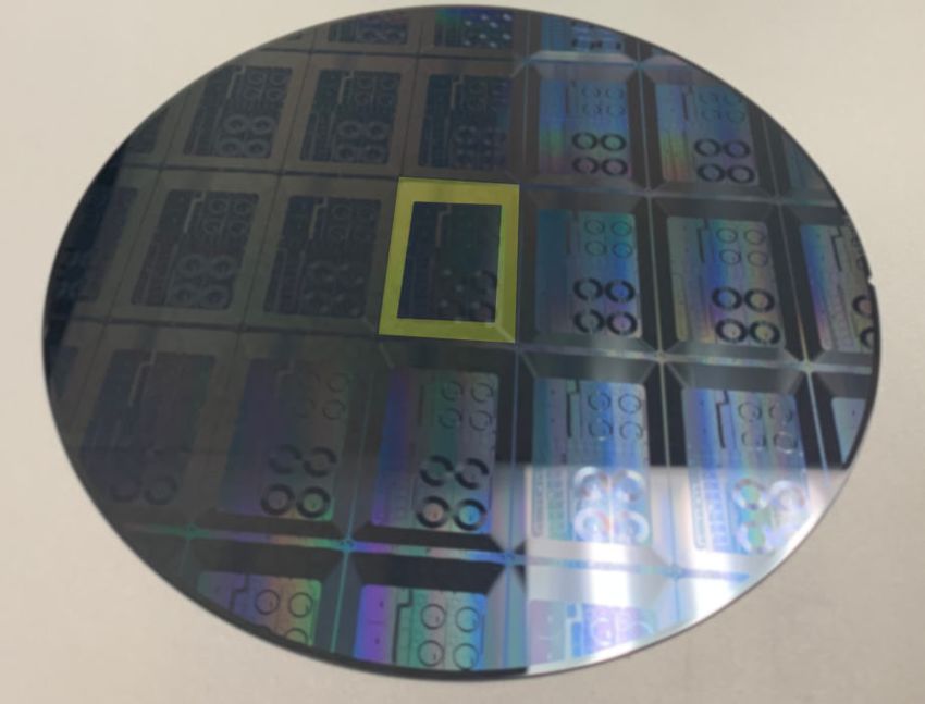
Fig. 2. Device measurement and model validation. (a) Fabricated
200 mm wafer with stitched delay lines 23 m in length on the perimeter
of each die. The delay line of the center die is highlighted. Each die 0.01
consists of two stitched reticles. The interior of each die is occupied
by test structures. (b) Micrograph of alignment test structure between 0.001
adjacent reticles. Each half of the mark is exposed separately; each mark 1 10 100
represents an additional 10 nm alignment bias between left and right
reticles. We estimate an alignment error below 20 nm. (c) Stitched Fig. 3. Simulated loss versus length of “abrupt” and “angled”
racetrack resonator test structure. (d) Micrograph of stitched wave- stitching at 100 nm alignment error for (a) 100 nm thick silicon nitride
guides in a resonator. (e) Measured stitching loss versus wavelength waveguides and (b) 220 nm thick silicon waveguides. To compare the
for each test structure. Nine configurations were measured, consisting loss and length of abrupt stitches with angled stitches, abrupt stitch
of three different stitch lengths, each evaluated for three mask offsets. loss is simulated as a function of waveguide width, while the length is
(f ) Comparison of measurement with simulation of our design at calculated as the length of the corresponding mode converters for each
±100 nm misalignment. waveguide width.Letter Vol. 46, No. 12 / 15 June 2021 / Optics Letters 2987
channel waveguides. In this stitch design, we adopt a 400 nm Data Availability. Data underlying the results presented in this paper are
single-mode waveguide width at the input and output of the not publicly available at this time but may be obtained from the authors upon
stitch, δMAX of 100 nm, and we again simulate the perform- reasonable request.
ance of our design as a function of stitch length L [Fig. 3(b)].
The abrupt stitch loss is simulated up to a waveguide width of
REFERENCES
14 µm. Our optimized design in this silicon waveguide platform
approaches 0.001 dB per stitch for a stitch length below 10 µm, 1. N. Margalit, C. Xiang, S. M. Bowers, A. Bjorlin, R. Blum, and J. E.
Bowers, Appl. Phys. Lett. 118, 220501 (2021).
compared to over 50 µm in the silicon-nitride-based design.
2. B. Buscaino, E. Chen, J. W. Stewart, T. T. Pham, and J. M. Kahn, J.
We attribute this reduction to the narrower waveguide width Lightwave Technol. 39, 1984 (2020).
of 400 nm, compared to 2.8 µm. This is because a narrower 3. S. Fathololoumi, D. Hui, S. Jadhav, J. Chen, K. Nguyen, M. Sakib,
optical mode, for the same angle θ, accumulates less phase error Z. Li, H. Mahalingam, S. Amiralizadeh, N. N. Tang, H. Potluri,
across its width due to the mismatched phase fronts at the angled M. Montazeri, H. Frish, R. A. Defrees, C. Seibert, A. Krichevsky,
junction. At a stitch length of just 6 µm, our silicon waveguide J. K. Doylend, J. Heck, R. Venables, A. Dahal, A. Awujoola, A.
Vardapetyan, G. Kaur, M. Cen, V. Kulkarni, S. S. Islam, R. Spreitzer,
stitch design achieves approximately 50-fold lower loss for the
S. Garag, A. Alduino, R. Chiou, L. Kamyab, S. Gupta, B. Xie,
same length, or approximately 50-fold smaller footprint at the R. Appleton, S. Hollingsworth, S. McCargar, and Y. Akulova, J.
same level of loss, compared to the abrupt stitching approach. Lightwave Technol. 39, 1155 (2021).
In conclusion, we presented a novel method for stitching 4. T. J. Seok, K. Kwon, J. Henriksson, J. Luo, and M. C. Wu, Optica 6,
photonic waveguides to enable seamless transitions between 490 (2019).
reticles. We demonstrated in both simulation and experiment 5. J. Sun, E. Timurdogan, A. Yaacobi, E. S. Hosseini, and M. R. Watts,
Nature 493, 195 (2013).
that it produces stitched waveguides with a smaller footprint
6. C. V. Poulton, M. J. Byrd, B. Moss, E. Timurdogan, R. Millman, and
and lower loss by over an order of magnitude compared to prior M. R. Watts, in Conference on Lasers and Electro-Optics (CLEO):
approaches. For delay lines and interferometric gyroscopes Applications and Technology (OSA, 2020), paper JTh4A-3.
where the waveguide crosses a stitching boundary multiple 7. J. Arrazola, V. Bergholm, K. Brádler, T. Bromley, M. Collins, I. Dhand,
times per round trip, ultralow stitching loss is critical. In our A. Fumagalli, T. Gerrits, A. Goussev, L. Helt, J. Hundal, T. Isacsson, R.
23 m long device, the 332 stitches contribute just 0.13 dB to the Israel, J. Izaac, S. Jahangiri, R. Janik, N. Killoran, S. Sumar, J. Lavoie,
A. Lita, D. Mahler, M. Menotti, B. Morrison, S. Nam, L. Neuhaus, H.
total loss. However, for optical switch and interconnect appli-
Qi, N. Quesada, A. Repingon, K. Sabapathy, M. Schuld, D. Su, J.
cations, no signal path should cross a stitching boundary more Swinarton, A. Sava, K. Tan, V. Vaidya, Z. Vernon, Z. Zabaneh, and Y.
than a handful of times, so the small stitch footprint is more Zhang, Nature 591, 54 (2021).
valuable. Indeed, an abrupt stitch limits the pitch of waveguides 8. J. Feldmann, N. Youngblood, M. Karpov, H. Gehring, X. Li, M.
crossing the reticle boundary to a value above the waveguide’s Stappers, M. Le Gallo, X. Fu, A. Lukashchuk, A. S. Raja, J. Liu, C.
width—over 10 µm in prior works [4]. In our approach, the Wright, A. Sebastian, T. Kippenberg, W. Pernice, and H. Bhaskaran,
Nature 589, 52 (2021).
width of the stitched waveguide can be kept close to the single-
9. W. Jin, Q.-F. Yang, L. Chang, B. Shen, H. Wang, M. A. Leal, L. Wu,
mode width, allowing a high density of waveguides to traverse M. Gao, A. Feshali, M. Paniccia, K. J. Vahala, and J. E. Bowers, Nat.
reticles. Furthermore, while our approach was developed for Photonics 15, 346 (2021).
the case of deep-UV stepper lithography in a foundry context, 10. J. F. Bauters, M. J. Heck, D. D. John, J. S. Barton, C. M. Bruinink, A.
we note that it could be applied to the contact, i-line stepper, Leinse, R. G. Heideman, D. J. Blumenthal, and J. E. Bowers, Opt.
and even E-beam lithography tools that are common in research Express 19, 24090 (2011).
11. C. G. Roeloffzen, L. Zhuang, C. Taddei, A. Leinse, R. G. Heideman, P.
contexts. W. van Dijk, R. M. Oldenbeuving, D. A. Marpaung, M. Burla, and K.-J.
Initially driven by demand for low-cost interconnects for Boller, Opt. Express 21, 22937 (2013).
datacenter networks and high-performance computing, PIC 12. C. Xiang, M. L. Davenport, J. B. Khurgin, P. A. Morton, and J. E.
performance and scale have grown dramatically in recent Bowers, IEEE J. Sel. Top. Quantum Electron. 24, 1 (2017).
years. Large-scale devices have emerged: high-radix optical 13. S. Srinivasan, R. Moreira, D. Blumenthal, and J. E. Bowers, Opt.
switches; OPAs for LiDAR, free-space communications, and Express 22, 24988 (2014).
14. S. Gundavarapu, M. Belt, T. A. Huffman, M. A. Tran, T. Komljenovic,
augmented/virtual reality displays; meshed interferometer net- J. E. Bowers, and D. J. Blumenthal, J. Lightwave Technol. 36, 1185
works for artificial intelligence, machine learning, and quantum (2018).
computation; and ultralow-loss delay lines and resonators for 15. T. Huffman, M. Davenport, M. Belt, J. E. Bowers, and D. J.
nonlinear optics and metrology. Many of these applications Blumenthal, in IEEE Photonics Conference (IEEE, 2016),
have already demonstrated PICs at or beyond the single reticle pp. 478–479.
limit, and will continue to grow as fabrication yields improve. 16. M. J. Van de Moosdijk, E. Van den Brink, K. Simon, A. Friz, G. N.
Phillipps, R. J. Travers, and E. Raaymakers, Proc. SPIE 4688, 858
We believe the low-loss multi-reticle PIC will soon become a (2002).
critical tool in the optical system designer’s toolbox. 17. A. Milton and W. Burns, IEEE J. Quantum Electron. 13, 828 (1977).
Funding. DARPA LUMOS (HR001-20-2-0044); Anello Photonics.
Disclosures. WJ: Anello Photonics (F,I,P). AF, MP: Anello Photonics
(I,E,P). JB: Anello Photonics (F).You can also read