Defect-states Passivation Strategy in Perovskite Solar Cells
←
→
Page content transcription
If your browser does not render page correctly, please read the page content below
E3S Web of Conferences , 01031 (2021) https://doi.org/10.1051/e3sconf/202124501031
AEECS 2021
Defect-states Passivation Strategy in Perovskite Solar Cells澳
Hongrui Hu 1, *
1Shanghai experiment international school, Shanghai, China
Abstract. In the modern era, energy demand rises dramatically accompanied by the rapid growth of our
population, causing urgent energy shortages and environmental issues around the globe. People turned their
attention to solar energy for an eco-friendly and economic solution, in which, perovskite solar cells emerged
and had caught a great deal of attention in the past decades for their promising and commercial development
potential. To fully release their capability for a high-performance device, defect mechanisms which are one
of the main factors inhibiting the efficiency and stability, as well as passivation strategies must be thoroughly
studied. In this review, the concept and formation mechanism of the defects are summarized, the
corresponding defect characterization techniques regarding their working principles and downsides were also
compared. Furthermore, substantial passivation strategies were discussed. Although perovskite solar cells still
have a long way to go, facing difficulties in a lot of other aspects, we believe that the research we are doing
now is of great significance in making perovskite into a real application.
1 INTRODUCTION several hundred-nanometer thick absorber layers were
sandwiched between the electron transport layer (ETL)
Perovskite solar cell is a kind of solar cell that employs and hole transport layer (HTL) without a mesoporous
hybrid organic-inorganic metal halide as core light- scaffold. Despite its shorter development period, it
harvesting materials. It has occupied a leading position provided an efficiency of over 15% and provide simplified
and become one of the hot spots in the photovoltaic device configurations at that time.[7] Inverted perovskite
research field owing to its economical manufacture costs, has a device structure known as “p-i-n”, in which HTL is
simple solution processing fabrication, and rapidly at the bottom of intrinsic perovskite layer i with ETL n at
boosting photoelectric conversion efficiency (PCE), the top, in which light was illuminated through the HTL
which has attracted great attention from the business surface. In recent years, a novel kind of multidimensional
market since its potential for next photovoltaic evolution. perovskite has become promising candidates to surmount
The PCE has skyrocketed from 3.8% [1] in 2009 to 25.5% several challenges in perovskite devices, especially, long-
[2] this year, with the help of strong light-harvesting term stability. Mostly, it forms a ruddlesden–popper
ability [2], small exciton binding energy[3], fast charge structure with the help of aliphatic or aromatic alkyl
transport properties[4], and prolonged charge carrier ammonium cation[8].
lifetime[5]. Perovskite is a special crystal structure with
the chemical components simplified in ABX3, generally,
in our case, A is small organic molecules or metal cations
(Cs+, MA+, FA+), B refers to divalent metal cations (Pb 2+,
Sn2+, Ge2+, Cu2+) and X represents halide (I-, Br-, Cl-). The
classical perovskite photovoltaic material is CH3NH3PbI3,
in which the halogen ions are located in the octahedral top
with the lead wrapped in the center of the octahedral cage,
and the organic methyl amino groups located at the top
angles of the face-centered cubic lattice.
From the lessons learned from dye-sensitized solar
cells (DSSCs), the first perovskite device structure was
mesoporous superstructure, in which a large number of
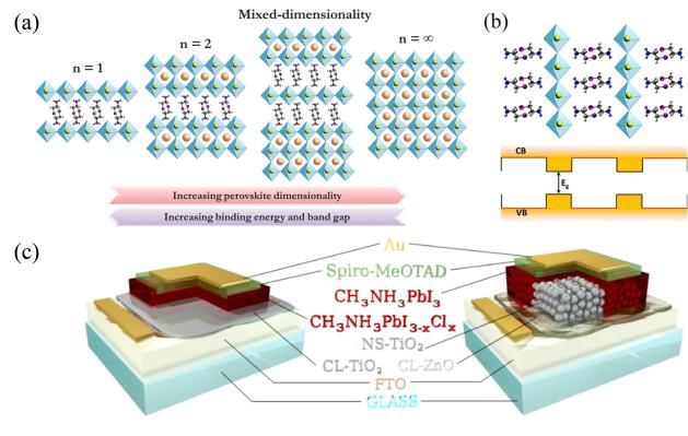
Fig.1. (a) The crystalline structure of multidimensional
mesoporous TiO2 were adopted to support the perovskite perovskites, including 2D perovskites (n=1 and 2, where n
materials, and also played a role in electron transport. [6] represents the metal halide lattices), mixed-dimensional
Further studies demonstrated the superior charge transport perovskites, and 3D perovskites (n=1). Adapted from Ref. [9].
properties of perovskite itself and led to the birth of the Copyright 2016 Wiley-VCH Verlag GmbH & Co.KGaA. (c)
planar structure. In a planar junction perovskite solar cell, Typical perovskite solar cell device structure: (Left) planar
* Corresponding author: hhr317@gmail.com
© The Authors, published by EDP Sciences. This is an open access article distributed under the terms of the Creative Commons Attribution License 4.0
(http://creativecommons.org/licenses/by/4.0/).E3S Web of Conferences , 01031 (2021) https://doi.org/10.1051/e3sconf/202124501031
AEECS 2021
structure, (Right) mesoporous scaffold. Adapted with and the vacancy created from the same ion); f, Schottky defect
permission from ref. (10). Copyright 2014 American Chemical (anion and cation vacancies occurring together); g,
Society substitutional impurity; h, interstitial impurity; i, edge
dislocation (line defect propagating along the axis
perpendicular to the page); j, grain boundary; and k, precipitate.
2 DEFECTS IN PEROVSKITE SOLAR
SYSTEM 2.1 Passivation Strategies in Perovskite Solar
Despite the fast advance in the perovskite performance, Cells
the existence of defects leads to compromised PCE due to For halide perovskites with un-passivated interfaces, large
non-radiative recombination centers and trap induced grain boundaries and high defect density would strongly
charge injection barriers, which results in a gap between enhance the activity of trap-assisted recombination
the current PCE and the theoretically deduced Shockley- channel, which is a major loss in halide perovskite-based
Queisser limit. ɉ 11 Ɋ The defects or trap-states have photovoltaics.[14] Trap assisted recombination at
negative impacts on both the electronic and optic interface defects is even more detrimental than grain
properties. In laser and LEDs, deep-level defects boundaries, by solely passivating interface traps, the PCE
encouraged non-radiative recombination and lower the can be enhanced by 40% [15]. When a defect state, lies
photoluminescence quantum yield, the radiative energetically within the semiconductor bandgap, there is a
recombination at shallow defects also broadened the likelihood that an approaching electron or hole will
emission spectrum. Nevertheless, defects significantly become captured or trapped. The trapped electron (or hole)
accelerate the efficiency drop under the outdoor is likely to be emitted, or de-trapped back to the
environment and hinder the long-term stability issues. conduction (or valence) band by phonon absorption if the
Therefore, studying, and depressing defects in perovskite activation energy is sufficiently small. However, if the
is a vital topic for perovskite future practical applications. activation energy is large, then it is more likely that the
The defects in semiconductors can be classified into trapped carrier will annihilate or recombine with an
several categories. Point defects are one of the most opposite carrier before it can be emitted. Therefore, as a
important ones, includes vacancies, interstitials, and kind of polycrystalline thin film, perovskite thin-film must
antisites, which are caused by missing atoms, extra atoms, have a low density of charge carrier traps (16). Controlling
and exchanged atoms, respectively. Aside from point charge carrier trapping is an extremely important issue in
defects, there can be line (one-dimensional) defects, where the development of high-performance solar cells.
lattice periodicity is discontinuous along a line. Defects Passivation, in physical chemistry and engineering,
can develop into even higher dimensions, such as two- refers to a material becoming “passive”, that is, less
dimensional surface defects and grain boundaries, and affected or corroded by the environment in which it will
three-dimensional voids and precipitates. The defects can be used. Passivation involves the application of an outer
be described according to two criteria. One is the layer of a shielding material as a micro-coating, created by
formation energy of defects, which determines the chemical reaction with the base material [17]. The
probability of a defect type to exist in the material. The transition process from the “active state” to the “passive
smaller the formation energy, the easier the defect can be state” by the formation of a passivating 㸚lm [18]. For
triggered and generated. Another criterion is the position perovskite solar cells, passivation generally refers to either
of the defect energy levels compared to the valence band chemical passivation, which reduces the defect trap states
maximum (VBM) and conduction band minimum (CBM). to optimize the charge transfer between various interfaces,
For energy levels close to the VBM or CBM, they are or physical passivation, which isolates certain functional
referred to as shallow-level traps while those located in the layers from the external environment to avoid degradation
middle third of the forbidden bandgap are referred to as of the device.
deep-level traps. Shallow-level traps can release the
trapped charge carriers back to the band edges especially
at elevated temperatures [12,13] whereas the deep-level 2.1.1 Surface passivation by Lewis acid/bases
traps cannot detrap charges easily.
Surface passivation for organic-inorganic halide
perovskite solar cells by introducing the Lewis bases
thiophene and pyridine were proposed, curbing the
formation of Pb defects and non-radiative recombination
centers, which largely increases the PL quantum yield, PL
lifetime as well as the PCE of the device. [19,20] The
possible nature of the passivation mechanism is that the
Lewis bases might donate electrons to bare Pb atoms
originated from halide vacancy. Another Lewis base IT激
M also helps to achieve an efficiency of 20.5% with a fill
factor of 81%, since it stabilizes the Pb octahedrons in the
ambient environment [21].
On the other hand, hole traps could be healed via Lewis
Fig. 2. Various kind of defects: a, perfect lattice; b, vacancy; c,
acid. Iodopentafluorobenzene (IPFB) is a type of Lewis
interstitial; d, anti-site substitution; e, Frenkel defect (interstitial
2E3S Web of Conferences , 01031 (2021) https://doi.org/10.1051/e3sconf/202124501031
AEECS 2021
acid that helps to coordinate halogen atoms[22,23] via (atomic layer deposition), or a chemical deposited TiCl 4
supramolecular halogen bonding.(24,25) By immersing layer. [52]
annealed halide perovskites in the IPFB and drying under Furthermore, lithium ions were adopted to facilitate
N2, the traps of halide perovskites can be effectively the electronic properties of the TiO2 mesoporous layer by
passivated, which prevents charge accumulation and reducing electronic trap states. Additionally, self-
recombination at the interface. assembled fullerene derivatives, pyridine, and other
semiconductor shell layers that possess high electron
mobility could also be brought in to help the passivation
2.1.2 Grain boundary passivation
of the TiO2 layer. [53-55]
Fullerene derivatives are a kind of famous superstar Aside from the functional materials involved in the
materials used in an organic photovoltaic system, while in operational devices, the selective electrodes could not be
perovskite devices, they were usually used in inverted p-i- ignored to fulfill the performance enhancement
n structured perovskite solar cells. The fullerene layers procedures. An ultra-thin Ni surface layer could be applied
deposit on the perovskite layers, eliminating photocurrent to the Au electrode that functioned as both a physical
hysteresis and improving the device performance. [26] An passivation barrier and a hole-transfer catalyst [56], which
ultra-thin PCBM layer was coated on the perovskite would enhance photocurrent density and substantially
surface, followed by heat treatment, during which the better water stability [57,58]
PCBM diffused into the grain boundaries, where plenty of
defects gathers. It passivates the PbI3 anti-site defects 2.1.5 Surface passivation for long-term stability
during the formation of perovskite grains.[27]
In perovskite, self-passivation is a superior property Long-term stability has always been a vital research topic
that achieves perovskite. There are three methods to from the very beginning when perovskite solar cells
introduce a PbI2 passivation layer at perovskite grain appear. Some organic materials that contain hydrophobic
boundaries. The first one is the self-induced formation of groups, such as polystyrene (PS) [42], poly(ethylene
PbI2 from the controlled degradation of pristine perovskite terephthalate) (PET), poly(methyl methacrylate) (PMMA)
thin films via thermal[28,29,30,31] or water vapor [43-45],Te 㸛 on [46,42], poly(4-vinyl pyridine) (PVP)
treatment [32-34]. The second is the preparation of a non- [46,47], polyvinylidene-tri 㸛 uoroethylene copolymer
stochiometric perovskite precursor solution with an excess (PVDF-TrFE) [42], and even ionic liquids [48], could be
of PbI2 (usually 3%-10% molar ratio relative to the brought to cover the surface. They have been used as
perovskite[35-38]; and the final one is the incomplete protective polymer film on perovskite thin-film/arrays,
reaction of PbI2 through a two-step solution or vapor and not only passivate surface defects but also block
reaction method[37-39] atmospheric moisture, allowing perovskite solar cells to
Another key component that constructs perovskite is sustain over 80% of their initial performance after 30 days
CH3NH3I (MAI), which could also be introduced to of storage in high moisture (50%) condition[70].
complete self-passivation. This process was achieved by
MAI vapor post-treatment, which was found to be an
efficient method to passivate defect sites on perovskite 2.2 Methods to evaluate the trap states properties
grain surface[40,41].
According to the abovementioned details about the trap-
states in perovskite solar systems, it could be readily found
2.1.3 Bulk Passivation via alky metal doping that basic knowledge about the trap-states is vital in
efficiency promotion strategy. Therefore, the priority is to
In perovskite devices, the photocurrent hysteresis capture the fruitful properties of the trap-states. Several
phenomenon is an inevitably involved issue that should be classical techniques are summarized herein, accompanied
addressed. In recent years, a universal strategy named alky by corresponding basic principles.
metal doping strategy is proposed. Time-resolved
photoluminescence (TRPL) and Photoluminescence
quantum efficiency (PLQE) measurements show that 2.2.1 Space-Charge-Limited-Current (SCLC)
potassium doping is an efficient procedure to perform trap
SCLC is a powerful method to estimate the density of
state passivation. The PCE of the passivated device would
defect states and charge mobility from measured current-
jump from 17.3% to 21.5%, accompanied by the
voltage characteristics, it can be determined by the product
enhancement of VOC (Open-circuit voltage) and JSC
of space-charge density derived from the permittivity of
(Short-circuit current density). Besides, the ion migration
the semiconductor[59]
is also inhibited in that observation, which strongly
Defects can trap and scatter the free charge carriers,
hindered the hysteresis.[49,50,51]
thus change the electrical properties of halide perovskites.
Under charge injections through ohmic contacts, it can be
2.1.4 Passivation of the charge carrier transport found that there are three distinct regions in the log-log
pathways current-voltage curve. [60] When the voltage is relatively
small, ܫĝܸ݊ with n=1. This is the first region called the
Trap states located at the surface of the selected Ohmic region. The second region is the trap-filled limit
transportation layer are also crucial aspects. The typical (TFL) region, where the applied voltage reaches a certain
ETL TiO2 could be passivated by an ultrathin layer of TiO2 threshold value ܸܶܮܨ, the defects become saturated and are
3E3S Web of Conferences , 01031 (2021) https://doi.org/10.1051/e3sconf/202124501031
AEECS 2021
not able to trap more free carriers. The resistance thus method depends on the dynamics of the trapping-
jumps to a lower value and n increases to above 3. The detrapping process as well as the relative position of defect
third region is called the Child region with n equals to 2 energy level and Fermi energy.
that follows the Mott-Gurney law[61]. The defects density
can be derived with the assumption that all defects are
filled, and injected charges can freely move, 3 CONCLUSIONS
2 0VTFL Perovskite cells have a promising potential in the future
ntrap 漏1漐 optoelectronic device market, although they are still
qL2 facing instability and limited PCE undersides. To make it
where ݊ ܽݎݐis the defect density, ߝ is the relative dielectric more competitive, we need a dedicated and
constant to vacuum, ߝ0 is the vacuum permittivity, ݍis the comprehensive understanding of the defect behavior and
electric charge and ܮis the thickness[62]. mechanism in perovskite cell using various theoretical and
Temperature-dependent SCLC can be used to defer the experimental methods such as DFT, SCLC mentioned
energy level of the defect relative to CBM and VBM, above, and from there we can devise the appropriate and
d ln( J ) effective ways for defect passivation, and rapid progress
Etrap could be made in the field so far. Currently, we have so
d ( kbT ) 1
漏2漐 many different strategies for passivation using different
with current density ܬ, temperature ܶand Boltzmann materials on different parts, we have surface passivation
constant ݇[ܤ63][64]. using Lewis base/ acid, grain boundary passivation using
fullerenes derivatives, bulk passivation through doping
with alkyl metal, and even passivating charge carrier
2.2.2 Density functional theory (DFT) calculation transport pathways. All these are crucial processes not
only to increase the PCE, hinder hysteresis, and also
The determined trap concentration via SCLC is not
improve long-term stability to make it a more resilient,
accurate as different charges cannot be differentiated, for
durable, and competitive device in the future.
instance, the potential of ion migration within the crystal
resulting in underestimation of trap concentration.
Knowing this situation, theoretical calculations, such as Reference
DFT methods, is necessary to explore the nature of traps
because it is not possible to find out the origin of 1. A.Kojima,;K.Teshima,Kenjiro;Y.Shirai,;T.,Miyasaka
imperfections experimentally. DFT is a computational ,"Organometal Halide Perovskites as Visible-Light
modeling method using supercells of a large number of Sensitizers for Photovoltaic Cells". J. Am. Chem. Soc,
atoms to investigate the electronic structure through 131, 17, 6050–6051(2009)
functionals of spatially dependent electron density. The 2. Giulia Lucarelli, Francesco Di Giacomo, Valerio
small formation energy of defect states in perovskite Zardetto, Mariadriana Creatore & Thomas M.
devices is estimated and the shallow distribution property Brown,Efficient light harvesting from flexible
is elucidated via DFT, which facilitates the strong trap perovskite solar cells under indoor white light-
states tolerance ability and prolongs the carrier lifetime in emitting diode illumination, Nano Research
perovskite devices. (65˅ volume 10, pages2130–2145(2017)
3. Krzysztof Galkowski, Anatolie Mitioglu, Atsuhiko
2.2.3 Thermal admittance spectroscopy (TAS) Miyata, Paulina Plochocka, Oliver Portugall, Giles
E.Eperon,JacobTse-Wei Wang,Thomas Stergiopoulos,
Defects could be deemed as an analog of small capacitors Samuel D. Stranks, Henry J. Snaith and Robin J.
since the trapping-detrapping behavior can be considered Nicholas, Determination of the exciton binding energy
as a charge-discharge process. By applying alternating and effective masses for methylammonium and
current (AC), the admittance of the target halide formamidinium lead tri-halide perovskite
perovskites will respond to the AC voltage. The relative semiconductors† Energy Environ. Sci., 9, 962-
position of the defect energy level to the Fermi level 970(2016)
determines the probability the defects are occupied or 4. Xiwen Gong, Ziru Huang, Randy Sabatini, Chih-
not[66]. Temperature and frequency-dependent Shan Tan, Golam Bappi, Grant Walters, Andrew
admittance could provide the density of trap states (tDOS) Proppe, Makhsud I. Saidaminov, Oleksandr Voznyy,
with a trap energy depth profile [67]by the following Shana O. Kelley & Edward H. Sargent,Contactless
formula: measurements of photocarrier transport properties in
Vbi dC perovskite single crystals,, Nature Communications
ntrap , E
qWD dk BT volume 10, Article number: 1591 (2019)
漏3漐
5. David Kiermasch, Philipp Rieder, Kristofer
Where ܸܾ݅ is the built-in heterojunction potential Tvingstedt, Andreas Baumann & Vladimir
barrier, ߱ is the AC frequency, ܥis the capacitance and Dyakonov,Improved charge carrier lifetime in planar
ܹ ܦis the depletion width of the space-charge region perovskite solar cells by bromine doping,Scientific
[68.69]. However, very deep traps or traps with long Reports volume 6, Article number: 39333 (2016)
thermal emission time cannot be detected since this
4E3S Web of Conferences , 01031 (2021) https://doi.org/10.1051/e3sconf/202124501031
AEECS 2021
6. Sining Yun, Yong Qin, Alexander R. Uhl, Nick photoluminescence and solar cell performance via
Vlachopoulos, Min Yin, Dongdong Li, Xiaogang Lewis base passivation of organic–inorganic lead
Han and Anders Hagfeldt ,new-generation integrated halide perovskites ACS nano,8,9815-21(2014)
devices based on dye-sensitized and perovskite solar 22. Jain S M, Qiu Z, Häggman L, Mirmohades M,
cells,Energy Environ. Sci., 11, 476-526(2018) Johansson M B, Edvinsson T and Boschloo G
7. Tze-Bin Song,Qi Chen,HuanpingZhou,Chengyang Frustrated Lewis pair-mediated recrystallization of
Jiang,Hsin HuaWang, Yang (Michael) Yang, CH3NH3PbI3for improved optoelectronic quality
Yongsheng Liu, Jingbi You and Yang Yang Perovskite and high voltage planar perovskite solar cells Energy
solar cells:film formation and Environ. Sci.9,3770-82(2016)
propertiesJ.Mater.Chem.A,3,9032[39] 39 (2015) 23. Yang G, Qin P,Fang G and Li G A Lewis Base激
8. V. Gonzalez-Pedro, E. J. Ju ́arez-P ́erez, W. S. Assisted Passivation Strategy Towards Highly
Arsyad,E. M. Barea, F. Fabregat-Santiago, I. Mora- Efficient and Stable Perovskite Solar Cells Sol.
Sero and J. Bisquert,Nano Lett.,14, 888–893.( 2014) RRL21800055(2018)
9. C. C. Stoumpos, D. H. Cao, D. J. Clark, J. Young, J. 24. Abate A, Saliba M, Hollman D J, Stranks S D,
M. Rondinelli, J. I.Jang, J. T. Hupp, M. G. Wojciechowski K, Avolio R, Grancini G, Petrozza A
Kanatzidis,Chem. Mater.28, 2852–2867(2016) and Snaith H J Supramolecular halogen bond
10. B. V. Beznosikov, K. S. Aleksandrov,,Crystallogr. passivation of organic–inorganic halide perovskite
Rep.45, 792–798(2000)S. N. Ruddlesden, P. solar cells Nano Lett.14,3247-54(2014)
Popper,Acta Crystallogr.11, 54–55(1958) R. E. 25. Abate A, Biella S, Cavallo G, Meyer F, Neukirch H,
Schaak, T. E. Mallouk,Chem. Mater,14, 1455– Metrangolo P, Pilati T, Resnati G and Terraneo G
1471(.2002) Halide anions driven self-assembly of
11. T. M. Koh, V. Shanmugam, J. Schlipf, L. Oesinghaus, haloperfluoroarenes:Formation of one-dimensional
P. Müller-Busch-baum, N. Ramakrishnan, V. Swamy, non-covalent copolymers J.Fluorine Chem.1301171-
N. Mathews, P. P. Boix, S. G. Mhaisal-kar,Adv. 7(2009)
Mater,28, 3653–3661.(2016) 26. A. Abate, M. Saliba, D.J. Hollman, S.D. Stranks, K.
12. V. Gonzalez-Pedro, E. J. Ju´arez-P´erez, W. S. Wojciechowski, R. Avolio, G. Grancini, A. Petrozza,
Arsyad,E. M. Barea, F. Fabregat-Santiago, I. Mora- H.J. Snaith, Supramolecular halogen bond
Sero andJ. Bisquert, Nano Lett., 14, 888–893, (2014) passivation of organic-inorganic halide perovskite
13. Sha W E, Ren X, Chen L and Choy W C,The solar cells, Nano Lett. 14,3247-3254. (2014)
efficiency limit of CH3NH3PbI3 perovskite solar 27. N.K. Noel, A. Abate, S.D. Stranks, E.S. Parrott, V.M.
cells Appl. Phys. Lett.106221104 (2015) Burlakov, A. Goriely, H.J. Snaith, Enhanced
14. Li W, Liu J, Bai F-Q, Zhang H-X and Prezhdo O V photoluminescence and solar cell performance via
Hole trapping by iodine interstitial defects decreases Lewis base passivation of organic inorganic lead
free carrier losses in perovskite solar cells: a time- halide perovskites, ACS Nano 8 9815e9821. (2014)
domain ab initio study, ACS Energy Lett.2,1270- 28. Y.H. Shao, Z.G. Xiao, C. Bi, Y.B. Yuan, J.S. Huang,
8(2017) Origin and elimination of photocurrent hysteresis by
15. Srimath Kandada A Ret al Nonlinear carrier fullerene passivation in CH 3 NH 3 PbI 3 planar
interactions in lead halide perovskites and the role of heterojunction solar cells, Nat. Commun. 5
defects JACS,138,13604-11(2016) 5784(2014)
16. Shao Y, Xiao Z, Bi C, Yuan Y and Huang J Origin 29. Pengjun Zhao, Byeong Jo Kim, Hyun Suk Jung
and elimination of photocurrent hysteresis by Passivation in perovskite solar cells: A review
fullerene passivation in CH3NH3PbI3planar Materialstoday Energy,7,267--286(2018)
heterojunction solar cells Nat. Commun.5,5784(2014) 30. T. Supasai, N. Rujisamphan, K. Ullrich, A.
17. Sherkar T S, Momblona C, Gil激Escrig L, Bolink H J Chemseddine, T. Dittrich, Formation of a passivating
CH 3 NH 3 PbI 3 /PbI 2 interface during moderate
and Koster L J A Improving perovskite solar cells:
heating of CH 3 NH 3 PbI 3 layers, Appl. Phys. Lett.
Insights from a validated device model Adv. Energy
103 183906(2013)
Mater.7,1602432(2017)
31. Q. Chen, H.P. Zhou, T.B. Song, S. Luo, Z.R. Hong,
18. X.X. Wu, M.T. Trinh, D. Niesner, H.M. Zhu, Z.
H.S. Duan, L.T. Dou, Y.S. Liu,Y. Yang, Controllable
Norman, J.S. Owen, O. Yaffe, J. Kudisch, X.Y. Zhu,
self-induced passivation of hybrid lead iodide
Trap states in lead iodide perovskites, J. Am. Chem.
perovskites toward high performance solar cells,
Soc.137 2089e2096(2015)
Nano Lett. 14 4158e4163(2014)
19. A.D. McNaught, A. Wilkinson, Compendium of
32. Q. Jiang, L.Q. Zhang, H.L. Wang, X.L. Yang, J.H.
Chemical Terminology,(1997)
Meng, H. Liu, Z.G. Yin, J.L. Wu,X.W. Zhang, J.B.
20. Passivation(chemistry),https://en.wikipedia.org/wiki/ You, Enhanced electron extraction using SnO 2 for
Passivation_(chemistry),(Accessed 13 November high-efficiency planar-structure HC(NH 2 ) 2 PbI 3 -
2017) based perovskite solar cells, Nat. Energy 2 1-7, (2017)
21. Noel N K, Abate A, Stranks S D, Parrott E S, 33. P. Cui, D. Wei, J. Ji, D. Song, Y. Li, X. Liu, J. Huang,
Burlakov V M, Goriely A and Snaith H J Enhanced
5E3S Web of Conferences , 01031 (2021) https://doi.org/10.1051/e3sconf/202124501031
AEECS 2021
T. Wang, J. You, M. Li, Highly efficient electron- 6 2503e2508. (2015)
selective layer free perovskite solar cells by 44. Q. Wang, Q. Dong, T. Li, A. Gruverman, J. Huang,
constructing effective pen heterojunction, Solar RRL Thin insulating tunneling contacts for efficient and
1 1600027,(2017) water-resistant perovskite solar cells, Adv. Mater.28
34. M.L. Petrus, Y.H. Hu, D. Moia, P. Calado, A.M.A. 6734e6739. (2016)
Leguy, P.R.F. Barnes, P. Docampo, The influence of 45. H. Deng, X.K. Yang, D.D. Dong, B. Li, D. Yang, S.J.
water vapor on the stability and processing of hybrid Yuan, K.K. Qiao, Y.B. Cheng,J. Tang, H.S. Song,
perovskite solar cells made from non-stoichiometric Flexible and semitransparent organolead triiodide
precursor mixtures, ChemSusChem 9,2699-2707. perovskite network photodetector arrays with high
(2016) stability, Nano Lett. 15 7963e7969.v
35. W.N. Peng, B. Anand, L.H. Liu, S. Sampat, B.E. 46. J. Li, J.J. Si, L. Gan, Y. Liu, Z.Z. Ye, H.P. He, Simple
Bearden, A.V. Malko, Y.J. Chabal, Influence of approach to improving the amplified spontaneous
growth temperature on bulk and surface defects in emission properties of perovskite films, ACS Appl.
hybrid lead halide perovskite films, Nanoscale 8 Mater. Inter. 8 32978e32983.( 2016)
1627e1634.(2016)
47. S. Kumar, A. Dhar, Accelerated thermal-aging-
36. Y. Lei, L.Y. Gu, W.W. He, Z.X. Jia, X.G. Yang, H.M. induced degradation of organometal triiodide
Jia, Z. Zheng, Intrinsic charge carrier dynamics and perovskite on ZnO nanostructures and its effect on
device stability of perovskite/ZnO mesostructured hybrid photovoltaic devices, ACS Appl. Mater. Inter.
solar cells in moisture, J. Mater. Chem. A 4 8 18309e18320 (2016)
5474e5481.(2016)
48. B. Chaudhary, A. Kulkarni, A.K. Jena, M. Ikegami, Y.
37. T.J. Jacobsson, J.P. Correa-Baena, E.H. Anaraki, B. Udagawa, H. Kunugita, K. Ema, T. Miyasaka, Poly(4-
Philippe, S.D. Stranks, M.E.F. Bouduban, W. Tress, K. Vinylpyridine)-based interfacial passivation to
Schenk, J. Teuscher, J.E. Moser, H. Rensmo, A. enhance voltage and moisture stability of lead halide
Hagfeldt, Unreacted PbI 2 as a double-edged sword perovskite solar cells, ChemSusChem 10
for enhancing the performance of perovskite solar 2473e2479, (2017)
cells, J. Am. Chem. Soc. 138 10331e10343.(2016)
49. L.J. Zuo, H.X. Guo, D.W. deQuilettes, S. Jariwala, N.
38. F.Z. Liu, Q. Dong, M.K. Wong, A.B. Djurisic, A.N. De Marco, S.Q. Dong, R. DeBlock, D.S. Ginger, B.
Ng, Z.W. Ren, Q. Shen, C. Surya, W.K. Chan, J. Wang, Dunn, M.K. Wang, Y. Yang, Polymer-modified halide
A.M.C. Ng, C.Z. Liao, H.K. Li, K.M. Shih, C.R. Wei, perovskite films for efficient and stable planar
H.M. Su, J.F. Dai, Is excess PbI 2 beneficial for heterojunction solar cells, Sci. Adv. 3 ,
perovskite solar cell performance? Adv. Energy Mater. e1700106.(2017)
6 1502206. (2016)
50. X. Huang, H. Guo, K. Wang, X.B. Liu, Ionic liquid
39. F.Y. Jiang, Y.G. Rong, H.W. Liu, T.F. Liu, L. Mao, W. induced surface trap-state passivation for efficient
Meng, F. Qin, Y.Y. Jiang, B.W. Luo, S.X. Xiong, J.H. perovskite hybrid solar cells, Org. Electron. 41
Tong, Y. Liu, Z.F. Li, H.W. Han, Y.H. Zhou, 42e48.(2017)
Synergistic effect of PbI 2 passivation and chlorine
51. :mojtaba abdi-Jalebi , Zahra andaji-Garmaroudi ,
inclusion yielding high open-circuit voltage
Stefania cacovich , camille Stavrakas , Bertrand
exceeding 1.15 V in both mesoscopic and inverted
Philippe Johannes m. richter , mejd alsari , Edward P.
planar CH 3 NH 3 PbI 3 (Cl)-based perovskite solar
Booker , Eline m. hutter , Andrew J. Pearson ,
cells, Adv. Funct. Mater. 26 8119e8127. (2016)
Samuele Lilliu , Tom J. Savenije ,håkan rensmo ,
40. S.M. Wang, W.W. Dong, X.D. Fang, Q.L. Zhang, S. Giorgio Divitini ,caterina Ducati, richard h. Friend &
Zhou, Z.H. Deng, R.H. Tao, J.Z. Shao, R. Xia, C. Samuel D. Stranks ,Maximizing and stabilizing
Song, L.H. Hu, J. Zhu, Credible evidence for the luminescence from halide perovskites with potassium
passivation effect of remnant PbI 2 in CH 3 NH 3 PbI passivation,Nature volume 555, pages497–501(2018)
3 films in improving the performance of perovskite
52. Stranks, S. D. & Snaith, H. J. Metal-halide
solar cells, Nanoscale 8 6600e6608. (2016)
perovskites for photovoltaic and light-emitting
41. T.Y. Zhang, N.J. Guo, G. Li, X.F. Qian, Y.X. Zhao, A devices. Nat. Nanotechnol. 10, 391–402 (2015)
controllable fabrication of grain boundary PbI 2
53. deQuilettes, D. W. et al. Photo-induced halide
nanoplates passivated lead halide perovskites for high
redistribution in organic–inorganic perovskite films.
performance solar cells, Nano Energy 26 50e56.
Nat. Commun. 7, 11683 (2016)
(2016)
54. Mohamad Firdaus Mohamad Noh, Chin Hoong Teh,
42. Z.M. Zhou, Z.W. Wang, Y.Y. Zhou, S.P. Pang, D.
Rusli Daik, Eng Liang Lim, Chi Chin Yap, Mohd
Wang, H.X. Xu, Z.H. Liu, N.P. Padture, G.L. Cui,
Adib Ibrahim, Norasikin Ahmad Ludin, Abd. Rashid
Methylamine-gas-induced defect-healing behavior of
bin Mohd Yusoff, Jin Jang and Mohd Asri Mat
CH 3 NH 3 PbI 3 thin films for perovskite solar cells,
Teridi The architecture of the electron transport layer
Angew. Chem. Int. Ed. 54 9705e9709. (2015)
for a perovskite solar cell ,J. Mater. Chem. C, ,6, 682-
43. B.S. Tosun, H.W. Hillhouse, Enhanced carrier 712(2018)
lifetimes of pure iodide hybrid perovskite via vapor-
55. M. Abdi-Jalebi, M.I. Dar, A. Sadhanala, S.P.
equilibrated Re-Growth (VERG), J. Phys. Chem. Lett.
6E3S Web of Conferences , 01031 (2021) https://doi.org/10.1051/e3sconf/202124501031
AEECS 2021
Senanayak, M. Gratzel, R.H. Friend, Monovalent 70. Shao Y, Xiao Z, Bi C, Yuan Y and Huang J Origin and
cation doping of CH 3 NH 3 PbI 3 for efficient elimination of photocurrent hysteresis by fullerene
perovskite solar cells, Jove J. Vis. Exp. 121 passivation in CH3NH3PbI3planar heterojunction
55307(2017) solar cells Nat. Commun.5,5784 (2014)
56. S.S. Mali, C.S. Shim, H.K. Park, J. Heo, P.S. Patil, 71. Li D, Shi J, Xu Y, Luo Y, Wu H and Meng Q
C.K. Hong, Ultrathin atomic layer deposited TiO 2 for Inorganic–organic halide perovskites for new
surface passivation of hydrothermally grown 1D TiO photovoltaic technology Natl. Sci. Rev.5,559-
2 nanorod arrays for efficient solid-state perovskite 76( 2017)
solar cells, Chem.Mater. 27 1541e1551(2015) 72. I. Hwang, I. Jeong, J. Lee, M.J. Ko, K. Yong,
57. J. Dong, X. Xu, J.J. Shi, D.M. Li, Y.H. Luo, Q.B. Enhancing stability of perovskite solar cells to
Meng, Q. Chen, Suppressing charge recombination in moisture by the facile hydrophobic passivation, ACS
ZnO-nanorod-based perovskite solar cells with Appl.Mater. Inter. 7 17330e17336 (2015)
atomic-layer-deposition TiO 2 , Chin. Phys. Lett. 32
078401(2015)
58. Pengjun Zhao, Byeong Jo Kim, Hyun Suk Jung
Passivation in perovskite solar cells: A review
Materialstoday Energy,7,267--286(2018)
59. P.M. Da, M.Y. Cha, L. Sun, Y.Z. Wu, Z.S. Wang, G.F.
Zheng, High-performance perovskite photoanode
enabled by Ni passivation and catalysis, Nano Lett. 15
3452e3457. (2015)
60. C.W. Wang, S. Yang, X. Chen, T.Y. Wen, H.G. Yang,
Surface-functionalized perovskite films for stable
photoelectrochemical water splitting, J. Mater. Chem.
A 5 910e913(2017)
61. Paul W. M. Blom 1 & Gert-Jan A. H. Wetzelaer,
Space-charge-limited electron and hole currents in
hybrid organic-inorganic perovskites Mohammad
Sajedi Alvar1,Nat Commun ;11:4023.(2020)
62. Shi Det al2015 Low trap-state density and long carrier
diffusion in organolead trihalide perovskite single
crystals Science347,519-22(2015)
63. Child C 1911 Discharge from hot CaO Physical
Review (Series I)32,492(1911)
64. Liu Zet al Chemical reduction of intrinsic defects in
thicker heterojunction planar perovskite solar cells
Adv.Mater 29 1606774(2017)
65. Srimath Kandada A Ret al Nonlinear carrier
interactions in lead halide perovskites and the role of
defects JACS138,13604-11(2016)
66. Adinolfi Vet a The In ϋ Gap Electronic State
Spectrum of Methylammonium Lead Iodide Singleϋ
Crystal Perovskites Adv. Mater.28,3406-10(l2016)
67. Zewen Xiao,,a Weiwei Meng,a,b Jianbo Wang,b and
Yanfa Yan,Defect Properties the Two-Dimensional
(CH3NH3)2Pb(SCN)2I2Perovskite: A Density
Functional Theory Study,Phys. Chem. Chem.
Phys., ,18, 25786-25790(2016)
68. Duan H-S, Zhou H,Chen Q, Sun P, Luo S, Song T-B,
Bob B and Yang Y The identification and
characterization of defect states in hybrid organic–
inorganic perovskite photovoltaics Phys. Chem.
Chem.Phys 17 112-6(2015)
69. Xiao Z, Dong Q, Bi C, Shao Y, Yuan Y and Huang J
Solvent annealing of perovskite ϋ induced crystal
growth for photovoltaic ϋ device efficiency
enhancement Adv. Mater.26 6503-9(2014)
7You can also read