Department of Physics and Astronomy University of Heidelberg - David Schledewitz 2021 Bachelor Thesis in Physics submitted by born in Witzenhausen ...
←
→
Page content transcription
If your browser does not render page correctly, please read the page content below
Department of Physics and Astronomy
      University of Heidelberg

          Bachelor Thesis in Physics
                submitted by

         David Schledewitz
       born in Witzenhausen (Germany)

                   2021
Measurement of the rate and angular distribution of
        cosmic muons with an ALPIDE telescope

     This Bachelor Thesis has been carried out by David Schledewitz at the
GSI Helmholtzzentrum für Schwerionenforschung GmbH, Darmstadt (Germany)
  and Physikalisches Institut Universität Heidelberg, Heidelberg (Germany)
                            under the supervision of
                           Prof. Dr. Silvia Masciocchi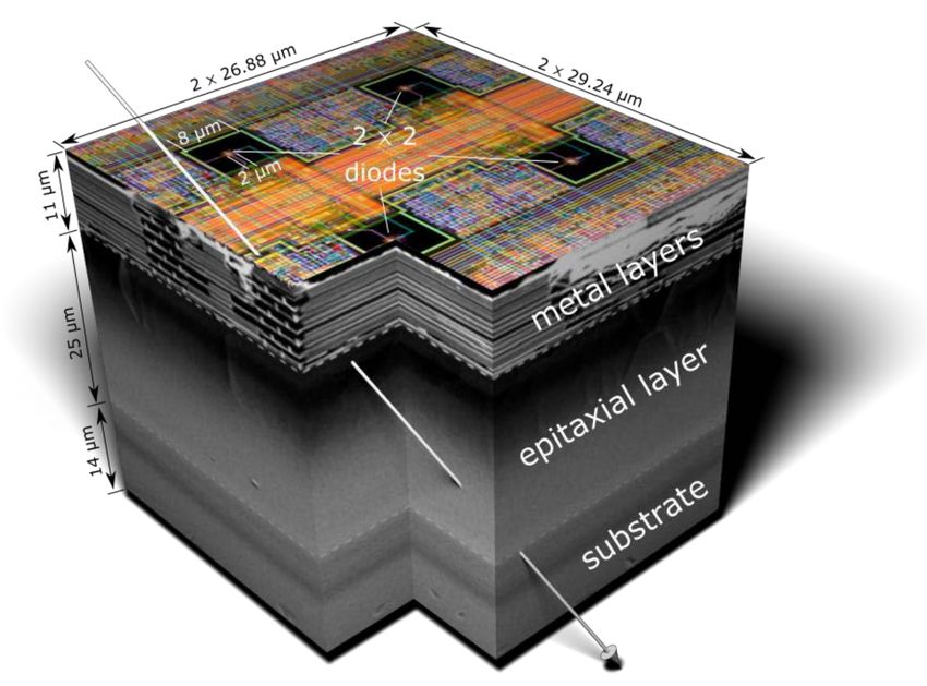
Abstract

In preparation for the planned upgrades during the LHC Long Shutdown 2, a new
generation of monolithic active pixel sensors (ALPIDE) was developed for the
new high-resolution Inner Tracking System of the ALICE detector. These ALPIDE
sensors have been rigorously tested and were proven to meet and exceed the
requirements for the next LHC runs.
Several tests were performed to investigate the response of the chips, including
measurements of cosmic muons. Of particular interest is the ability to detect and
track such particles reliably. In this thesis, a seven plane ALPIDE telescope was
used to detect cosmic muons and investigate their angular distribution.
First, the identification and analysis of hits are done by comparing the detected
muon rate with the theoretical one. Next, a track reconstruction and visualization
method is employed, and the quality of the tracks is verified. Consequently, the
angular distribution is assessed within the detectable zenith angle range, from 0°
to 28°. In the range of more than 4°, the distribution is found to agree rather well
with the expected angular distribution of cosmic muons.
Finally, limitations and possible improvements of the experimental setup are
discussed to measure the angular distribution with more precision and a wider
angular range.
Zusammenfassung

Im Rahmen des geplanten Upgrades während des LHC Long Shutdown 2 wurde
eine neue Generation von Pixeldetektoren (ALPIDE) für das neue hochauflösende
Inner Tracking System des ALICE-Detektors entwickelt. Diese ALPIDE-Sensoren
wurden intensiv getestet, um zu bestätigen, dass sie die Anforderungen des ALICE-
ITS-Upgrades erfüllen.
Es wurden viele Tests durchgeführt, unter anderem Messungen an kosmischen
Myonen, um die Antwort der Chips zu untersuchen. Hierbei ist insbesondere, die
Fähigkeit solche Teilchen zuverlässig zu erkennen und ihre Spur zu rekonstruie-
ren, interessant. In dieser Arbeit wurde ein ALPIDE-Teleskop mit sieben Sensoren
verwendet, um kosmische Myonen zu detektieren und ihre Winkelverteilung zu
untersuchen.
Zunächst wurde die Zuverlässigkeit der Messungen sichergestellt, indem die Rate
an detektierten Myonen mit der entsprechenden theoretischen Rate verglichen
wurde. Als Nächstes wurde eine Methode zur Rekonstruktion und Visualisierung
der Spuren eingesetzt, um deren Qualität zu überprüfen. Daraufhin wurde die
Winkelverteilung innerhalb des detektierbaren Winkelbereichs (0° - 28°) ausgewer-
tet. Es stellte sich heraus, dass die Winkelverteilung, im Bereich von mehr als 4°,
gut mit den Erwartungen für kosmische Myonen übereinstimmt.
Abschließend werden Einschränkungen und mögliche Verbesserungen des experi-
mentellen Aufbaus diskutiert, um die Winkelverteilung präziser und für einen
größeren Winkelbereich zu messen.

Contents

1   ALICE at the LHC                                                                       1
    1.1   ALICE . . . . . . . . . . . . . . . . . . . . . . . . . . . . . . . . . . .       1
    1.2   ITS . . . . . . . . . . . . . . . . . . . . . . . . . . . . . . . . . . . . .     3

2   Particle interactions with matter                                                       7
    2.1   Standard model of particle physics . . . . . . . . . . . . . . . . . . .          7
    2.2   Cosmic radiation . . . . . . . . . . . . . . . . . . . . . . . . . . . . .        8
          2.2.1   Cosmic rays in the atmosphere . . . . . . . . . . . . . . . . .           8
          2.2.2   Muons at sea level . . . . . . . . . . . . . . . . . . . . . . . .       10
    2.3   Physics of particle detection . . . . . . . . . . . . . . . . . . . . . . .      11
    2.4   Semiconductors . . . . . . . . . . . . . . . . . . . . . . . . . . . . . .       14
          2.4.1   Properties of intrinsic semiconductors . . . . . . . . . . . . .         14
          2.4.2   Doped semiconductors . . . . . . . . . . . . . . . . . . . . .           16
          2.4.3   The pn-junction . . . . . . . . . . . . . . . . . . . . . . . . . .      17

3   The ALice PIxel DEtector (ALPIDE)                                                      20
    3.1   Principle of MAPS . . . . . . . . . . . . . . . . . . . . . . . . . . . .        20
    3.2   ALPIDE detector structure . . . . . . . . . . . . . . . . . . . . . . . .        23
    3.3   Principle of operation of the in-pixel circuitry . . . . . . . . . . . . .       24
    3.4   Chip tests . . . . . . . . . . . . . . . . . . . . . . . . . . . . . . . . . .   26

4   Measurement of cosmic muons                                                            29
    4.1   Motivation . . . . . . . . . . . . . . . . . . . . . . . . . . . . . . . . .     29
    4.2   Experimental setup . . . . . . . . . . . . . . . . . . . . . . . . . . . .       30
    4.3   Data acquisition and processing . . . . . . . . . . . . . . . . . . . . .        31

5   Theoretical calculations of the muon rate and its angular distribution                 34
    5.1   Muon rate . . . . . . . . . . . . . . . . . . . . . . . . . . . . . . . . .      34
          5.1.1   Preliminary considerations . . . . . . . . . . . . . . . . . . .         34
          5.1.2   Estimated total flux . . . . . . . . . . . . . . . . . . . . . . . .     36
          5.1.3   Detection rate of n-plane-events . . . . . . . . . . . . . . . .         41

                                                                                            I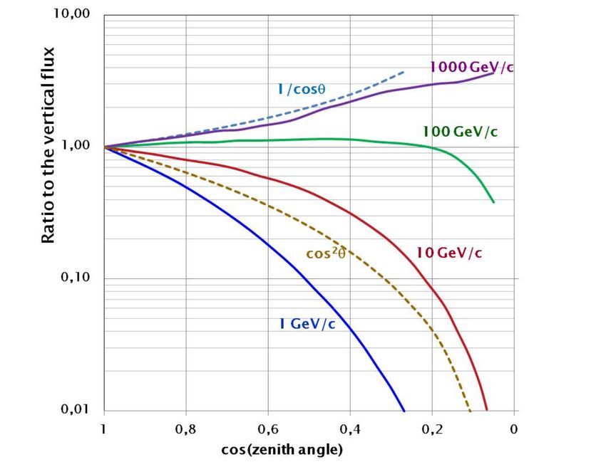
CONTENTS
5.2 Angular distribution . . . . . . . . . . . . . . . . . . . . . . . . . . . 43
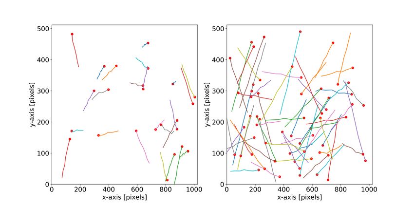
6 Analysis of the angular distribution 46
6.1 Event-based analysis without tracking . . . . . . . . . . . . . . . . . 46
6.2 Tracking based analysis . . . . . . . . . . . . . . . . . . . . . . . . . 50
6.2.1 Alignment . . . . . . . . . . . . . . . . . . . . . . . . . . . . . 51
6.2.2 Track fitting for quality assurance . . . . . . . . . . . . . . . 52
6.2.3 Determining the angular distribution . . . . . . . . . . . . . 55
7 Discussion and conclusion 60
Appendices 65
A 66
A.1 Calculation of the muon energy loss traversing the ALPIDE telescope 66
A.2 Maximum possible zenith angle of muons traversing the entire
ALPIDE telescope . . . . . . . . . . . . . . . . . . . . . . . . . . . . 67
A.3 Additional figure to the analysis . . . . . . . . . . . . . . . . . . . . 68
IIChapter 1
ALICE at the LHC
In the world of science, many interesting open questions exist. Driven by their
inquisitiveness, many scientists dedicate their lives to answering those questions,
or at least address them. Therefore, many research facilities were founded to focus
on different fields of science, like medical science, astronomy, or meteorology, to
name only a few. One of these facilities is the Conseil Européen pour la Recherche
Nucléaire, better known as CERN, near Geneva in Switzerland. It was founded in
1954 and is dedicated to high-energy physics research and aims to answer some of
the fundamental scientific issues about our universe [1]. Today CERN’s 27 kilome-
ter long Large Hadron Collider (LHC) is the world’s largest particle accelerator. In
September 2008, the first proton beam was injected into the accelerator [2].
Two separate beampipes are built in the LHC in which particles are accelerated in
opposite directions, whereby they approach the speed of light. At specific points
in the LHC, the resulting particle beams are colliding. At each collision point, an
experiment is set and detectors are built to measure the outcome of the collisions.
At LHC four main experiments are placed, LHCb 1 , ATLAS2 , CMS3 , and ALICE4 .
Next, the ALICE experiment will be discussed in more detail.
1.1 ALICE
The main objective of ALICE (A Large Ion Collider Experiment) is studying collisions
of heavy ions. Even though it was initially the only experiment dedicated to
heavy-ion physics, meanwhile all other three main experiments are also studying
heavy-ion collisions. Examples for investigated collision systems are lead-lead
(Pb-Pb), proton-lead (p-Pb), and proton-proton (p-p).
1 Large Hadron Collider beauty
2A Toroidal LHC ApparatuS
3 Compact Muon Solenoid
4 A Large Ion Collider Experiment
11.1. ALICE Figure 1.1: Schematic view on the ALICE detector [3]. Abbreviations are explained below or can be found here [4]. To detect the particles produced in these collisions, ALICE uses an advanced detector system with total dimensions of 16 m × 16 m × 26 m and an approximate weight of 10 000 t. The detector is built around the interaction point (IP), where the particle collisions take place. A schematic view on the detector is given in figure 1.1. The innermost detector, directly surrounding the beampipe, is the Inner Tracking System (ITS). It consists of six layers of silicon detectors. The ITS acts as the first part of the tracking system, determining the position of particles traversing the detector with high resolution, thereby identifying the position of primary and secondary vertices of the short-lived particles produced in the collisions. During the Long Shutdown 2 (LS2), it is replaced by a new generation of pixel detectors as part of the ALICE upgrade. More details to this detector will follow in section 1.2. In ALICE, the Time Projection Chamber (TPC) follows the ITS, which is the central particle tracking system of ALICE. Particles traversing the gas-filled chamber of the TPC ionize the gas, and hence the resulting free electrons drift in the applied electric field of the chamber towards the endcap. There, the arrival time and position of the electrons are measured. With the energy deposited, the trajectory of the initial traversing particle can be reconstructed and allows Particle IDentification (PID). The Transition Radiation Detector (TRD) is the last part of the tracking system of ALICE. The TRD detects the transition radiation of electrons traversing thin layers 2
CHAPTER 1. ALICE AT THE LHC

of radiator materials. Hence, electrons can be discriminated from other charged
particles, which also leads to an improvement of PID.
The Time Of Flight (TOF) is the next detector layer of ALICE. The TOF consists of
Multigap Resistive Plate Chamber (MRPC) layers. Like most of the outer detector
layers of ALICE, it functions as an instrument for PID.
The High Momentum Particle Identification Detector (HMPID) is a further part of
the PID system. It is based on Ring Imaging Cherenkov (RICH) counters. Here
the Cherenkov radiation of fast traveling charged particles (p T 5 >1 GeV/c) is de-
tected. This detector complements the PID capabilities of TOF for high momentum
particles with p T >1 GeV/c.
The next detector layers are the two electromagnetic calorimeters.
The PHOton Spectrometer (PHOS) and the ElectroMagnetic Calorimeter (EMCal) aim
at measuring the energy of electrons and photons entering them.
Lastly, the Alice COsmic Ray DEtector (ACORDE) is used as a trigger for calibration
and alignment of ALICE and furthermore for studying high-energy cosmic rays.
A few more detectors are installed in ALICE, like the Muon Spectrometer and the
ForWard Detectors (FWD). Detailed information for these and also the previously
mentioned detectors can be found here [4].

To exploit the full potential of the LHC for studying heavy ion collisions, ALICE is
upgraded during the LS2 [5]. After the LS2, the LHC increases its luminosity and
eventually reaches a Pb-Pb collision rate of up to 50 kHz. The proposed enhance-
ments of the ALICE detector, combined with the significant increase of luminosity
provided by the LHC, allow a detailed and quantitative characterization of the
high density and high temperature phase of strongly interacting matter, as well
as the exploration of new phenomena in this matter. Therefore, high-precision
measurements of rare processes at low transverse momenta are required, which
can be achieved by enhancing ALICE’s low-momentum vertexing and tracking
capabilities, as well as increasing extensively the data taking rate.

1.2     ITS

The ITS is the innermost detector system of ALICE, with the purpose of tracking
and reconstructing of primary and secondary vertices, which are the points, where
particles collide or disintegrate. With the energy deposited in the detector, the ITS
also contributes to the PID.

  5 transverse   momentum

                                                                                   3
1.2. ITS To meet the requirements of the ALICE upgrade, amongst other detector systems, a new high-resolution ITS was developed. It provides a very efficient tracking, both in standalone mode and with the TPC, over a wider momentum range with special focus on very low momenta. Furthermore, the vertex reconstruction and the impact parameter, which is the distance of closest approach between a reconstructed track and the corresponding primary vertex and depends on the tracking and vertexing performance, is significantly improved. Another important development is the enhancement of the read-out rate capabilities to exploit the full expected Pb–Pb collision rate. These enhancements of the ITS are reached by the new highly developed detector technology, the so-called Monolithic Active Pixel Sensor (MAPS). The properties of the detector will be explained in detail in chapter 3. In the following, the advantages of the new compared to the former ITS are depicted, whereby the references are taken from [6]. Beampipe Besides the detector enhancement, also the beampipe diameter reduction is an essential part of the upgrade. The beampipe diameter is downsized from 29 mm to 19.2 mm. Due to this reduction, the distance of the first detector layer to the collision point can be lowered. Thickness Not only the beampipe, but also the thickness of the detector layers is reduced from 350 µm to 50 µm compared to the previous generation. As a result, the first layer of the ITS upgrade can be placed at an average distance to the collision point (radial position) of 23.4 mm, which is a vast improvement to the 39 mm of the former detector. In combination with the beampipe thickness reduction, this enhancement is particularly important to improve the impact parameter, since the tracking takes place at a closer distance to the collision point. Moreover, the reduced material budget leads to a decreased energy loss of particles traversing the detector layers, which reduces the scattering of low momentum particles. Pixel density Another improvement with direct impact on the tracking precision is the increased pixel granularity. Due to the new detector technology, the pixel dimensions of, for example, the first detector layer can be reduced by a factor of 50, from 50 µm × 425 µm down to 20 µm × 20 µm. Read-out speed As already mentioned, one of the key requirements for the ITS upgrade was to increase the read-out rate from 1 kHz (with close to 100% dead time) of the former ITS to at least 50 kHz to cope with the maximum rate of Pb-Pb 4
CHAPTER 1. ALICE AT THE LHC
collisions achievable after the LS2. With a read-out rate of up to 100 kHz for Pb-Pb
collisions, the upgraded ITS even exceeds the requirements by a factor of two.
Accessibility One last main upgrade compared to the previous detector genera-
tion is the accessibility of the ITS during the yearly shutdowns for maintenance and
repair interventions. Due to this feature, the preservation of high-quality measure-
ments of the ITS can be assured, unlike with the former ITS.
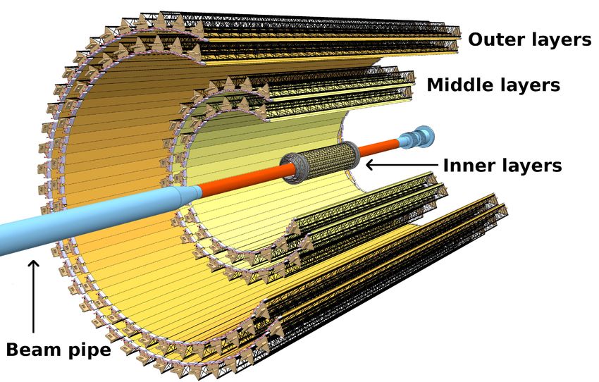
Figure 1.2: Schematic layout of the ITS upgrade [7].
Figure 1.2 depicts the detector layout of the upgraded ITS. The new ITS consists of
seven detector layers, which are further separated in an Inner and an Outer Barrel.
The three innermost layers are located in the Inner Barrel close to the beampipe.
The remaining four layers are located in the Outer Barrel, whereby the Outer
Barrel is segmented in two middle and two outer layers. The triangular-shaped
structure in each detector layer, shown in figure 1.2, is the so-called Stave, which
is an azimuthally segmented detector unit. It includes the supporting structure
of the sensors, a cooling system, energy supply, and a hybrid integrated circuit
(HIT). The HIT consists of a flexible printed circuit (FPC), which bounds the Pixel
Chips and a few passive components. Additionally, each Stave of the Outer Barrel
is segmented in two halves, named Half-Stave, each consisting of several modules
glued on a cooling unit. The radial positions of the detector layers can be seen in
figure 1.3, where a schematic cross-section of the Inner and Outer Barrel is shown.
51.2. ITS More details regarding the whole ITS upgrade can also be found here [6, 4]. Figure 1.3: Schematic cross-section layout of the ITS upgrade [8]. On the left the Inner Barrel and on the right the Outer Barrel is shown. Minimum, middle and maximum radial positions in mm are indicated for each detector layer. Before going into the functionality of the MAPS detector, the physics of parti- cle interaction with matter will be introduced in chapter 2, which is crucial to understand how particles and their properties can be measured in the detector. 6
Chapter 2

Particle interactions with matter

2.1    Standard model of particle physics
In order to understand the processes of particles interacting with matter and
especially with detectors, the basic principles of the Standard Model (SM) of
particle physics have to be introduced.
The SM describes the elementary particles that constitute matter and the funda-
mental forces which mediate their interaction [9]. It consists of twelve fermions,
which are particles with spin 1/2, and their corresponding anti-particles. It is com-
pleted by four gauge bosons with spin 1, which are the carriers of the fundamental
forces, and the spin 0 Higgs boson. A schematic overview of the 17 elementary
particles of the SM is given in figure 2.1.
As illustrated, the fermions are further divided into two groups of six particles
respectively, called leptons and quarks. In figure 2.1 fermions are sorted in rows
with the same properties, like spin and charge, except for their mass. In these
subgroups with there is a mass ordering, such that particles with higher mass
belong to a higher generation. In contrast to leptons, which exist freely, quarks
have to form bound states with other quarks to form so-called hadrons. There are
two types of hadrons:
   • Mesons: hadrons consisting of a quark and an anti-quark, e.g. π ± , π 0 , K ± ,
     K0 .

   • Baryons: hadrons consisting of three quarks, e.g. p, n, Λ0 , ∆0 .
Separating a quark from its bound state requires a high amount of energy. If this
energy is applied to a hadron, new quark-antiquark-pairs are created that can
form new bound states with the hadron’s initial quarks. Most of these hadrons are
unstable and decay into stable particles like electrons and protons.
There are four fundamental forces: electromagnetic interaction, weak interaction,
strong interaction, and gravity. However, gravity is not included in the SM.

                                                                                   7
2.2. COSMIC RADIATION Figure 2.1: Standard model of elementary particles with the 12 fundamental fermions and 5 bosons [10]. The shading indicates which gauge boson interacts with which fermion. Therefore, the gauge bosons of the SM are mediators for the remaining three fundamental interactions. The gluon carries color charge and is the mediator of the strong interaction, which couples only to quarks and is responsible for the confinement of quarks in bounded states. The photon is the mediator of the electromagnetic interaction, which couples to all charged fermions. The charged W ± bosons and the uncharged Z boson are the mediators for the charged- and neutral- current weak interaction, respectively. These bosons couple to all fermions and are the reason for nuclear decay, as well as the interaction of neutrinos with matter [9]. With the knowledge of the fundamental particle interactions the creation of cosmic radiation can be discussed in the following section. 2.2 Cosmic radiation 2.2.1 Cosmic rays in the atmosphere Cosmic radiation consists of stable and charged high energy particles, such as electrons, protons, helium, and more rarely heavy nuclei like carbon, oxygen, and iron [11]. Protons are the dominant constituents and make up 90% of the cosmic radiation. All these particles have in common that they were created in stars and 8
CHAPTER 2. PARTICLE INTERACTIONS WITH MATTER

accelerated by the explosions of those astrophysical sources. These particles are
called Primary Cosmic Radiation.
When entering the atmosphere, cosmic rays interact with the air nuclei and pro-
duce new particles. These secondary particles are still highly energetic and, therefore,
interact further with the atmosphere and create more particles. The approximate
particle distribution in different regions of the atmosphere is shown in figure 2.2.

Figure 2.2: Estimated fluxes (perpendicular to the Earth’s surface) of cosmic rays
in the atmosphere with E > 1 GeV. The points show measurements of muons
with Eµ > 1 GeV [11].

As shown in this figure, the most dominant particles in the top part of the atmo-
sphere are protons and neutrons. In the atmosphere they interact with atmospheric
molecules, and mesons are produced. In deeper atmospheric regions muons and
neutrinos are the most abundant particles. Those particles are produced in the
decay chains of charged mesons like pions and kaons in high atmosphere regions
[11]. The most common decays leading to muons are the pion decays by the weak
interaction:

                                                                                      9
2.2. COSMIC RADIATION
π + → µ+ + ν̄µ (2.1)
π − → µ− + νµ (2.2)
2.2.2 Muons at sea level
Muons are mostly produced in the high layers of the atmosphere at altitudes
of around 15 km. While traversing the atmosphere muons lose around 2 GeV of
their energy due to ionization (see section 2.3). This energy loss affects the energy
spectrum at sea level for small energies. Besides the energy loss in the atmosphere,
the energy and angular distribution of muons is dependent on their production
energy spectrum, and their lifetime (τµ ≈ 2.2 × 10⁻⁶ s) [11, 12].
Figure 2.3a represents the vertical integral muon momentum spectrum at sea level.
This represents the muon flux perpendicular to the Earth’s surface at different
momenta. The spectrum is nearly flat below 1 GeV/c. The intensity starts to
decrease at around 1 GeV/c. At momenta above 100 GeV/c the muon intensity
drops even steeper since pions in this energy region tend to interact more with the
atmosphere than decaying into muons.
(a) Absolute vertical integral momentum
(b) Angular distribution of muons at the
spectrum of muons in the range 0.2 < pµ <
ground for different muon momenta [14].
1000 GeV/c at sea level [13]. The veritcal in-
tegral intensity of muons is the muon flux
perpendicular to the Earth’s surface.
Figure 2.3: Momentum and angular distribution of muons at sea level
Next, figure 2.3b shows the angular distribution for muons at sea level with
different momenta. The angular distribution varies significantly for different
momenta. The distribution is steep at low energies, and the flux decreases with
increasing angle. The reason for the decreasing flux at large angles in this energy
10CHAPTER 2. PARTICLE INTERACTIONS WITH MATTER
region is that the muons have to traverse a longer distance through the atmosphere
before reaching the ground. Therefore, the energy loss by ionization increases,
which increases the minimum energy of a muon to reach the ground. For high
energies the distribution is nearly flat or even increases with increasing zenith
angle since the muon energy loss does not play a dominant role anymore at high
energies. The increasing flux for larger angles at very high energies is caused by
pions. As already stated, pions tend to interact with the atmosphere instead of
decaying at very high energies. However, at larger angles the distance over which
pions can decay and the probability of decaying in the atmosphere increases. As
a result, also the muon flux increases. Taking into account that the mean energy
for muons at sea level is around Eµ ∼ 4 GeV, the overall angular distribution is
approximately a ∼ cos2 (θ )-distribution, where θ is the zenith angle [11].
2.3 Physics of particle detection
In order to detect particles that are produced in cosmic showers or in high-energy
collisions, particle detectors have to be built. High energetic charged particles
propagating through matter lose energy mainly by ionization. In this process
the particles interact electromagnetically with the atomic electrons of the material
through which they pass. Besides ionization, other energy-loss processes can occur,
depending on the energy and type of a particle. However, muons lose energy
primarily through ionization over a wide momentum range. The Bethe-Bloch
formula describes the mean energy loss per unit path length through ionization
for all charged particles, but the electron [15].
2me c2 β2 γ2 Wmax
dE 2Z1 1 2 δ( βγ)
− = Kz ln −β − (2.3)
dx A β2 2 I2 2
z: charge of incident particle
K: constant factor
Z: charge number of traversed medium
A: atomic mass of traversed medium
me : electron mass
c: speed of light
I: mean excitation energy of traversed medium
δ: density correction of traversed medium
Wmax : maximum energy transfer in a single collision
Here, β = v/c represents the relative velocity and γ = √ 1 the Lorentz factor of
1− β2
the incident particle. h−dE/dx i represents the mass stopping power with the units
112.3. PHYSICS OF PARTICLE DETECTION MeV g−1 cm2 . With equation (2.3) the material-density independent stopping power can be determined. The linear stopping power is defined as ρ h−dE/dx i where ρ is the density of the traversed medium in g cm−2 . With the exception of density, the rate of ionization energy loss does not depend significantly on the properties of the traversed material. Figure 2.4a shows the mean energy loss through ionization for different materials as a function of βγ and the muon momentum, respectively. (a) Mean energy loss rate in different (b) Contributions to the energy loss of materials. Radiative effects are not in- muons in rock [16]. cluded [15]. Figure 2.4: Mean energy loss rate through ionization and influence of radiative effects. There are three different regions of the energy loss distribution which are relevant. First, at low momenta around 0.1 to 1 βγ the energy loss decreases with ∼ 1/β2 for increasing particle momenta. A broad minimum is reached at a βγ value of 3 to 4. Particles with a mean energy loss close to this minimum are called minimum-ionizing-particles (MIPs). After the minimum the energy loss increases due to the relativistic flattening and extension of the incident particle’s electric field. At even higher momenta the electric field polarizes the medium, limiting the field extension and hence damps the relativistic rise of the energy loss. The Bethe-Bloch formula, as described in equation (2.3), is valid in the region 0.1 . βγ . 1000. Outside of this region of validity, the Bethe-Bloch formula does not accurately describe the energy loss anymore and corrections have to be considered. At βγ & 1000 radiative effects begin to dominate over ionization, as shown in figure 2.4b. These processes are e+ e− pair production, bremsstrahlung, and photonuclear interaction. Another limitation for the use of the Bethe-Bloch formula is the thickness of the traversed medium. As mentioned above, the Bethe-Bloch formula describes 12
CHAPTER 2. PARTICLE INTERACTIONS WITH MATTER

the mean energy loss through ionization of charged particles traversing matter.
However, in thin layers, strong fluctuations from the mean energy loss occur,
which are described by the Landau model. This model describes the energy loss
probability density function f (∆/x ), which is also referred to as energy straggling
function. Here, ∆ is the amount of energy that an incident particle will lose on
traversing a layer of thickness x.

Figure 2.5a shows the straggling functions for 500 MeV pions in silicon for different
layer thicknesses. The figure indicates the most probable energy loss rate and the
mean energy loss rate, which is calculated by the Bethe-Bloch formula. For thin
layers the most probable and the mean energy loss rate differ significantly. As
a consequence, the Bethe-Bloch formula cannot describe the energy loss in thin
layers and the Landau model should be used. Figure 2.5b compares the energy
loss distribution described by the Bethe-Bloch formula and by the Landau model
for different thicknesses of a silicon layer. After the minimum, the energy loss
distribution of the straggling functions approaches a plateau, the so-called Fermi
plateau. Therefore, muons in the energy range of a few GeV to a few hundred GeV
have approximately the same energy loss traversing a thin silicon layer [15].

(a) Straggling functions in silicon for     (b) Bethe dE/dx and the Landau most prob-
500 MeV pions, normalized to unity at the   able energy loss per unit thickness for
most probable value ∆p/x. w is the full     muons traversing silicon. Radiative losses
width at half maximum.                      are excluded.

Figure 2.5: Energy loss fluctuations in thin layers described by the Landau distri-
bution [15].

                                                                                   13
2.4. SEMICONDUCTORS
2.4 Semiconductors
2.4.1 Properties of intrinsic semiconductors
Energy band structure Semiconductors are crystalline materials whose outer
shell electrons show an energy band structure. The conduction band is the energy
band with the highest energy. Electrons in this band are detached from their
initial lattice atoms, can move freely through the crystal, and as a result cause the
conductive behavior of the material. Another band is the valence band, which is
located at a lower energy level. Electrons in this band are still bound to their lattice
atoms. These energy bands can overlap or be separated. In the separated case the
region between the energy bands is referred to as energy gap. There are no energy
levels available for electrons to occupy in the energy gap. As a consequence, an
electron in the valence band needs a certain amount of energy to overcome the
energy gap and to excited into the conduction band. The energy gap value is
determined by material properties. However, it also depends on the temperature
and the pressure [17].
Figure 2.6a shows different configurations for the energy band structure. Materials
with a large energy gap are called insulators. In insulators at room temperature
all electrons are usually in the valence band and cannot be thermally excited into
the conduction band. In conductors the energy bands overlap and thus, electrons
can easily be excited into the conduction band. In semiconductors an energy gap
exists, which is small enough for some electrons to get thermally excited into the
conduction band at sufficient temperatures.
(a) Energy band structure of conductors,
insulators, and semiconductors [18]. (b) Covalent bonding in silicon [19].
Figure 2.6: Semiconductor properties
Charge carriers At 0 K, a semiconductor’s valence band is fully occupied and all
electrons participate in the covalent bond between the atoms. Figure 2.6b shows
an illustration of the covalent bonding in a pure (intrinsic) silicon semiconductor.
14CHAPTER 2. PARTICLE INTERACTIONS WITH MATTER
However, at temperatures close to room temperature valence electrons can get
thermally excited into the conduction band, leaving a hole at their former position
in the bonding. A neighboring valence electron can fill this hole, leaving a hole at
its original position. As this process continues, the hole appears to move through
the lattice. Relative to the negatively charged valence electrons the hole appears
as a moving positive charge carrier. Thus, the electric current in semiconductors
arises from two sources: the free electrons moving in the conduction band and the
holes moving through the valence band.
Besides the creation of new electron-hole pairs, also the recombination of already
existing electrons and holes takes place. Therefore, the concentration of electron-
hole-pairs reaches an equilibrium under stable environmental conditions. The
intrinsic concentration ni of electrons (or holes) is proportional to:
− Eg
3/2
ni = T exp (2.4)
2kT
Here, Eg is the energy gap at 0 K, k the Boltzmann constant, and T the temperature
[17]. In silicon, the required energy for an electron to be excited into the conduction
band is Eg = 3.6 eV [20]. At room temperature (300 K) the intrinsic charge carrier
concentration is in the order of ni ≈ 1.5 × 10¹⁰ m−3 [17].
Mobility If an electric field is applied to the semiconductor, the electrons and
holes drift through the semiconductor with the drift velocity νe and νh , respectively.
The drift velocities are defined as
νe = µe E
(2.5)
νh = µh E
where µe and µh represent the mobilities of the charge carriers and E the mag-
nitude of the applied electric field. The mobilities are dependent on the mate-
rial, the temperature, and the electric field for very high electric fields. In sili-
con, for E < 103 V cm−1 the mobilities are independent from the electric field.
At room temperature the mobilities in silicon are µe = 1350 cm2 V−1 s−1 and
µh = 480 cm2 V−1 s−1 [17]. With the mobilities, the resistivity of a semiconductor
can be determined:
1 1
ρ= = (2.6)
σ e(nµe + pµh )
Here, σ is the conductivity of the semiconductor, e is the elementary charge,
and n and p are the concentrations of free electrons and holes. In the case of
152.4. SEMICONDUCTORS intrinsic semiconductors they are equal to the intrinsic charge carrier concentration n = p = ni . The resistivity of intrinsic silicon at 300 K is ρ ≈ 230 kΩ cm [17]. 2.4.2 Doped semiconductors An intrinsic semiconductor has an equal number of free electrons and holes. By adding impurity atoms with a different number of valence electrons, this balance can be changed. In this process, which is referred to as doping, the impurity atoms integrate themselves into the intrinsic semiconductor crystal lattice. This new structure is called doped or extrinsic semiconductor. In a doped semiconductor atoms with an additional valence electron are called donors since they provide an additional electron. On the other hand, atoms with fewer valence electrons than the intrinsic material provide an additional hole and are called acceptors. The lattice structure and the modified energy band structure of the two types of doped semiconductors are illustrated in figure 2.7. Figure 2.7: (a) Addition of donor impurities. The impurities add excess electrons to the crystal and create donor impurity levels in the energy gap. (b) Addition of acceptor impurities. Acceptor impurities create an excess of holes and impurity levels close to the valence band [17]. In the situation of figure 2.7a the excess electrons can occupy an intermediate discrete energy level created in the energy gap, which is created by the impurity atoms. From this energy level it can more easily excite into the conduction band and thus increase the number of negative charge carriers and the conductivity of the semiconductor. The dominant type of charge carriers in a semiconductor is called the majority charge carrier, while the less occurring type is called the minority. Such semiconductors, in which electrons are the majority charge carriers, are referred to as n-type semiconductors. 16
CHAPTER 2. PARTICLE INTERACTIONS WITH MATTER

In the situation of figure 2.7b the holes are the majority charge carriers and the
electrons the minority charge carriers. These materials are called p-type semicon-
ductors. The concentration of charge carriers for both types is given by

                                                 − Eg

                            np =   n2i      3
                                         = T exp        .                       (2.7)
                                                 kT
Since the semiconductor is still neutral, the positive charges have to equal the
negative charges in the crystal:

                                 ND + p = NA + n                                (2.8)

where ND and NA represent the donor and acceptor impurity concentrations.
In n-type silicon, for example, only donors would be present and thus NA = 0.
With n  p the negative charge carrier concentration is n ' ND . Therefore, the
resistivity of an n-type semiconductor would become

                                              1
                                     ρ=            .                            (2.9)
                                            eND µe
The calculations for a p-type semiconductor can be performed analogously [17].

2.4.3   The pn-junction

An elementary part of building semiconductor detectors and electronic devices is
the formation of a junction between an n-type and a p-type semiconductor. The
difference in the concentration of electrons and holes between the two differently
doped materials causes an initial diffusion of electrons into the p-doped region
and holes into the n-doped region. As a consequence, the diffused electrons
and holes recombine with the corresponding majority charge carriers and lead
to a potential difference between the two regions. The p-type region becomes
negatively charged and the n-type region becomes positively charged. The now
charged regions create an electric field gradient, which stops the diffusion process,
leading to an equilibrium state. In this state the contact region of the material is
depleted of charge carriers and is therefore called depletion region or space charge
region. If electrons or holes are created in the depletion region, they will be
accelerated out of this region by the electric field.
Figure 2.8 illustrates the pn-junction with a depletion region. The figure also
depicts the idealized distribution of the charge density, the electric field, and the
potential. The width of the depletion region can be calculated with the Poisson
equation

                                                                                  17
2.4. SEMICONDUCTORS
Figure 2.8: A pn-junction in thermal equilibrium. Distributions of the charge
density, the electric field, and the potential difference are plotted [21].
d2 V ρ( x )
2
=− (2.10)
dx e
where e is the dielectric constant and the idealized charge density distribution is
eN
D − xn < x < 0
ρ( x ) = (2.11)
−eN 0 < x < xp
A
Here, e is the electron charge, and xn and x p are the depths of the depletion region
in the n-doped and p-doped side, respectively. The calculated depletion depth d is
s
2e ND + NA
d = xn + x p = ∆V (2.12)
e ND NA
where ∆V represents the built-in voltage (compare figure 2.8). The whole calcu-
lation is detailed in [17]. Using equation 2.9, it can be shown that the depletion
depth d (equation 2.12) is related to the resistivity ρ in the following way:
18CHAPTER 2. PARTICLE INTERACTIONS WITH MATTER
ρ · ∆V
p
d∼ (2.13)
For particle detection purposes, the depletion region should be as large as possible
since particles produce a signal mainly in this region. Therefore, high impedance
silicon is preferred for the detector design, as it leads to an increased depletion
depth (see equation 2.13). According to equation 2.13, another opportunity to
enlarge the depletion region is to increase the potential difference in the pn-
junction. In order to achieve this, a reverse-bias voltage can be applied to the
junction by connecting a negative voltage to the p-region and a positive voltage
to the n-region. This voltage will attract the majority charge carriers on each side
from the junction to the margin of the material. In this process the depletion region
is increased by
s
2e ND + NA
d= (∆V + V ) (2.14)
e ND NA
where V is the applied reverse bias voltage. Equation 2.13 can be extended in the
same way:
q
d∼ ρ · (∆V + V ) (2.15)
With the reverse-voltage applied to the junction, the width of the depletion region
can be extended up to a few mm. Apart from the larger depletion region, also the
charge collection efficiency is increased due to the stronger electric field [17].
19Chapter 3 The ALice PIxel DEtector (ALPIDE) In this chapter the ALice PIxel DEtector (ALPIDE) is discussed. This detector is developed and designed for the ALICE ITS upgrade (see section 1.2) and is used within the scope of this thesis. 3.1 Principle of MAPS MAPS and hybrid sensors Semiconductor sensors are often used in particle physics experiments as part of the particle tracking systems, including the LHC experiments ATLAS, CMS, LHCb, and ALICE. Compared to other tracking detec- tor systems, e.g., gas detectors, some advantages of semiconductor detectors are the small utilized space, the read-out speed, and a high spatial resolution [20, 22]. Typically hybrid pixel detectors are used, where the silicon sensor layer is bump- bonded to the read-out electronics, which process the signal (see figure 3.1). With this structure a large depletion region can be produced in the sensor layer. There- fore, a high amount of electron-hole pairs can be produced and collected, leading to a greater signal amplitude. This technology also has restrictions in terms of material thickness, costs, and pixel size, which limit the spatial resolution of the detector. In order to overcome these limitations, a new sensor technology was developed, where the read-out electronics and the sensor are merged into one single silicon layer. One model of this detector type is shown in figure 3.2a and is referred to as Monolithic Active Pixel Sensor (MAPS). Here, monolithic means that the read-out electronics and the sensor are on the same substrate. Active means that at least one amplifier is included in the in-pixel electronics. The MAPS still has disadvantages. The reduced material thickness leads to a smaller signal compared to the hybrid sensor due to less charge collection. 20
CHAPTER 3. THE ALICE PIXEL DETECTOR (ALPIDE)

However, this detector technology meets the requirements of heavy-ion experi-
ments and is therefore used for the newest generation of the inner tracking system
of ALICE (see section 1.2) [20, 6].

Figure 3.1: Transverse section of a hybrid pixel. The pixel consists of a Si-sensor
(bottom layer) bump-bonded to read-out electronics (upper layer). The grey line
indicates a particle track [20].

Signal detection One type of MAPS detectors, the ALPIDE, consists of three
main layers. These layers are depicted in the transverse section of a pixel cell in
figure 3.2a. The bottom layer is a highly p-doped substrate (p++ 1 ), which acts as a
reflective barrier for electrons in the middle layer due to the built-in voltage (see
section 2.4.3). This middle layer consists of a p− -doped2 material and is referred
to as epitaxial layer. In this layer the main charge production and collection takes
place. On top of the epitaxial layer n-type and p-type implants are located, which
are referred to as n-wells and p-wells. N-wells which are directly connected to the
epitaxial layer act as charge collecting diodes. Only in the close environment of the
collection diodes the epitaxial layer is depleted (see the white region in figure 3.2a).
  1A  p+ -doped material has a significantly higher concentration of dopants than a p-doped
material. The same is valid for p++ -doped compared to p+ -doped materials.
  2 A p− -doped material has a significantly lower concentration of dopants than a p-doped

material.

                                                                                        21
3.1. PRINCIPLE OF MAPS
To increase the depleted region, a small voltage3 is applied to the collection diode.
The depletion region can be further increased by applying an additional reverse
bias voltage4 VBB (also called back-bias voltage). The p-wells are hosting the
circuitry of the pixel sensor and prevent the electrons from the epitaxial layer from
entering and interfering with the circuitry. Moreover, some MAPS detectors, like
ALPIDE, provide a complex in-pixel circuitry by implementing PMOS5 transistors.
They can only operate on n-wells, which have to be isolated from the epitaxial
layer to prevent charge collection by the n-well. The separation is achieved by an
additional p-well layer, referred to as deep p-well [20, 23].
(b) 3D transverse section of a 2 × 2
(a) Transverse section of an ALPIDE MAPS pixel cell MAPS pixel matrix belonging to
[20]. the ALPIDE chip [20].
Figure 3.2: Illustrations of ALPIDE MAPS pixel cells
If a charged particle traverses the detector, as shown in figure 3.2a, it loses energy
due to ionization and creates electron-hole pairs in the silicon layers. As mentioned
above, electrons which are created in the epitaxial layer (p− -doped) do not diffuse
into the bottom p++ -doped layer and the p-wells (p+ -doped). Therefore, the
electrons will diffuse thermally through the epitaxial layer until they reach the
depletion region of the n-well diode, where they are collected and start drifting
in the electric field. The recombination of electrons and holes can be neglected
in non-irradiated detectors. Electrons which are created in the p-wells or in the
bottom layer can easily diffuse into the epitaxial layer and hence can also be
collected by the diode. If enough charge is collected, the signal is processed in the
in-pixel circuitry (see section 3.3) and the pixel registers a hit [20, 24].
3 In
case of the ALPIDE the voltage is up to 1.8 V[20].
4 Measurements with ALPIDE are performed with reverse bias voltages of up to −6 V [6]. In
this thesis, a reverse bias of −6 V is used.
5 p-type metal-oxide semiconductor
22CHAPTER 3. THE ALICE PIXEL DETECTOR (ALPIDE)
3.2 ALPIDE detector structure
Figure 3.2b shows the transverse section of a 2 × 2 MAPS pixel matrix belonging to
an ALPIDE chip. A single ALPIDE pixel cell has the dimensions 29.24 µm × 26.88 µm
(X x Y) and a thickness of 50 µm. The thickness of the sensitive epitaxial layer
amounts to 25 µm. On top of the implants of the epitaxial layer are metal layers,
which provide the in-pixel circuitry and are responsible for the signal transfer
to the chip logic. The pixel structure continues in X- and Y-direction creating a
pixel matrix. An entire ALPIDE chip measures 3 cm × 1.5 cm and contains 524 288
sensitive pixels arranged in a matrix of 1024 columns (X) and 512 rows (Y). The
chip matrix structure from the circuits side is shown in figure 3.3a. Looking at the
figure, the pixel rows are numbered from 0 to 511 arranged from the top to the
bottom of the chip. The columns are numbered from 0 to 1023 arranged from left
to right. The row and the column of a pixel determine its address[25].
(b) ALPIDE chip regions. Modified from
(a) ALPIDE architecture. Modified from fig- figure in [25].
ure in [25].
Figure 3.3: ALPIDE structure
The readout from a pixel is executed in the first instance by the Priority Encoder.
A Priority Encoder is connected to the pixels of two columns. Hence 512 Priority
Encoders are integrated on a single chip. The two pixel columns connected by
one Priority Encoder are referred to as a double column (see figure 3.3a). Every
pixel of a double column has an index (see first double-column in figure 3.3a),
defining the address of the pixel. The Priority Encoder selects one pixel with a
registered hit in the related double-column and generates its address. The address
of a pixel is sufficient to describe its state since the response of a pixel is binary -
either a hit is registered or not. After the address is generated, it is transmitted
further to the periphery. The periphery controls the entire chip and takes care of
233.3. PRINCIPLE OF OPERATION OF THE IN-PIXEL CIRCUITRY
biassing and readout of the chip. After transmitting the pixel address, the Priority
Encoder clears the memory and selects the next pixel of the double-column with
a registered hit. This procedure repeats until the addresses of all pixels, which
registered a hit, have been transmitted to the periphery and the pixel memories
have been reset. Thus, the position of every pixel can be defined by the number
of the double-column according to the whole chip (0 to 511 from left to right, see
figure 3.3a) to identify each pixel during the readout [25].
The pixel readout on the level of the whole chip is organized in 32 regions (512 × 32
pixels). Each region consists of 16 double-columns and their Priority Encoders.
Every region has a readout module in the periphery, which can execute the readout
of one double-column at a time in this region. Having 32 of such readout modules
working in parallel allows the simultaneous readout of 32 double-columns [25].
3.3 Principle of operation of the in-pixel circuitry
Signal processing The signal processing inside a pixel and how it is controllable
is now discussed. Each pixel has components which translate the charge produced
by an incident particle into a readable signal for the Priority Encoder. A simplified
layout of the in-pixel circuitry is shown in figure 3.4. In the input stage there is the
collection diode, collecting the charge which is generated in the epitaxial layer by
an incident particle. Moreover, a pulse injection capacitance is implemented to
inject a voltage, which simulates an incident particle to test the in-pixel-circuitry
(see section 3.4). The reset removes the voltage continuously6 , which is accumu-
lated by an incident particle or a voltage injection.
If charge is collected or a test pulse is injected, a voltage pulse propagates into the
analog front-end stage of the pixel (see figure 3.4, bottom left). The front-end stage
consists of an amplifier and a discriminator, which process the signal. First, the in-
put pulse is shaped to a signal with a peaking time of ∼ 2 µs (see figure 3.4, bottom
middle). In the discriminator the signal is compared to an adjustable threshold.
If the signal exceeds the threshold, a discriminated pulse with a typical duration
of up to 10 µs is passed to the next stage. In the last stage the signal is stored in
the in-pixel memory. The in-pixel memory consists of three hit storage registers
which are referred to as Multi Event Buffer (MEB). To store the hit information in
the MEB, a strobe signal is applied additionally to the discriminator output. If
the two signals are in coincidence (see figure 3.4, bottom right), the discriminator
output state is latched into one of the registers. Now the hit information can be
read out by the Priority Encoder.
6 Figure
3.4 (bottom left) shows the voltage accumulation over the period t f ' 10 ns and the
subsequent reset to the regular voltage over the period tr > 100 µs. This results in a voltage pulse
24CHAPTER 3. THE ALICE PIXEL DETECTOR (ALPIDE)
Figure 3.4: Schematic illustration of the ALPIDE in-pixel electronics and signal
shaping [25].
Digital-to-analog converter In the front-end of each pixel, several Digital-to-
Analog Converters (DAC) exist to adjust bias voltages and currents. For instance,
the signal shape or the threshold can be tuned by changing the 8-bit DAC parame-
ters (number from 0 to 255). The DACs are controlled globally for the entire chip,
meaning if one DAC is changed, it will be changed for all pixels on the chip. A
detailed scheme of the analog front-end of a pixel is shown in figure 3.5. In total
11 DACs are located in the pixel front-end. The threshold is controlled by three
different DACs: VCASN, ITHR, and IDB. VCASN influences the baseline volt-
age proportionally. This means that for increasing VCASN the baseline voltage
increases and, hence, the threshold decreases. ITHR determines the shape of the
amplified signal (see figure 3.4, bottom middle). For higher ITHR the pulse width
and height are reduced. This results in an increasing threshold for increasing
ITHR. IDB controls the current through its transistor (M7, see figure 3.5) propor-
tionally. A signal passes only to the PIX OUT B node if the charge deposit from a
traversing particle is sufficiently high to overcome the current setting IDB of M8.
Hence the threshold increases for higher IDB [25].
To determine the threshold, the injection of a variable amount of charge into the
front-end is necessary (see section 3.4). This is done by analog pulsing. In this
process a voltage is applied to the capacitor Cinj (see figure 3.4). The voltage
pulse is defined as the difference between the parameters VPULSE H IGH and
VPULSE LOW. Both have a maximum value of 1.8 V and are set by 8-bit DACs.
Hence the voltage can be varied in steps of 7 mV which corresponds to 10 electron
charges (e− ), considering the nominal value of Cinj = 230 aF [25].
253.4. CHIP TESTS
Figure 3.5: ALPIDE analog front-end scheme [25].
3.4 Chip tests
Threshold test One of the key parameters to control the chip performance is the
charge threshold. In general, a threshold defines a minimal physical value that has
to be supplied to a system to trigger a specific reaction. In this case, the threshold
defines the minimum charge needed to trigger a hit. On the ALPIDE sensor, the
threshold can be determined for each pixel of the chip. As discussed in section
3.3, the in-pixel threshold is controlled by the parameters VCASN, ITHR, and
IDB. These DACs are set the same to all pixels, as mentioned above. To determine
the threshold for a given set of these parameters, a test charge can be injected
by analog pulsing (see section 3.3). A threshold test performs multiple charge
injections for each tested pixel. The amount of injected charge Qinj varies in an
adjustable range [25, 20]. For example, charges can be injected in the range of 0 to
200 electron charges in steps of 10 electron charges (in DAC values: from 0 to 20
in steps of 1). For every charge configuration, the injection is repeated Ninj times.
For each test charge configuration Qinj,i a number Nhit,i ≤ Ninj of injections result
in a pixel hit. For small test charges, almost no pixel hits occur. With increasing
amounts of charge, the number of pixel hits rises until it reaches the maximum
number of Ninj . This can be seen in figure 3.6.
Here, the ratio of hits Nhit,i /Ninj of one pixel is plotted as function of the injected
charge Qinj,i . In an ideal case, a step-function-distribution could be expected. But
due to the random thermal motion of charge carriers and the resulting signal noise,
26CHAPTER 3. THE ALICE PIXEL DETECTOR (ALPIDE)
Figure 3.6: Example of the threshold measurement of one pixel: Nhit,i /Ninj as
a function of Qinj,i . The red line is the error function fit. The blue line is its
derivative, which is a Gaussian. The standard deviation of the Gaussian represents
the electronic noise of the pixel. [20].
the distribution is smeared and shaped like a s-curve. Since the noise is expected
to be Gaussian, the error function (erf) can be fitted to the data:
Qinj − µ
1
f ( Qinj ) = 1 + er f √ (3.1)
2 2σ
Here, µ represents the threshold and σ represents the noise of the measured
pixel. With the fit parameters, the threshold can be determined, which is defined
as the charge at which half of the injections result in a hit (Nhit,i /Ninj = 0.5).
Even with an identical set of parameters (DACs) for all pixels, the determined
threshold can vary from pixel to pixel. This is caused by minor fluctuations during
the manufacturing process of the in-pixel circuitry. Therefore the threshold for
the entire chip is defined as the average of the single pixel thresholds. Usually,
not every pixel of the chip is tested during the threshold test, but a fraction
of a few percent of all pixels. The pixels are thereby randomly chosen out of
each chip region. To control the number of tested pixels, two parameters exist.
PIXPERREGION controls the number of pixels per region in which the charge
is injected simultaneously. Values from 1 to 32 are possible, where a value of 1
corresponds to 1 pixel per region and 32 corresponds to a complete row. The
second parameter N MASKSTAGES controls how often the injection of charge in
a set of pixels per region (controlled by PIXPERREGION) is repeated. Thereby, a
new random set of pixels is chosen in every repetition. To test the entire chip, the
273.4. CHIP TESTS
mask has to be staged 16384/PIXPERREGION times. Any lower number leads
to a lower portion of pixels which will be scanned.
This procedure is done for every set of the parameters VCASN, ITHR, and IDB.
By varying one parameter while the other parameters stay the same, threshold
maps can be produced. These maps can be used for the chip threshold calibration
afterwards.
Noise occupancy test Another important test for the right calibration of the chip
is the noise occupancy test. In contrast to the threshold test, no charge is injected.
The test just applies a selectable number of triggers Ntrg and counts the number of
hits Nhit in the absence of an external stimulus [26]. With this test the Fake-Hit Rate
(FHR) can be determined. The FHR is defined as
Nhit
FHR = (3.2)
Npix · Ntrg
where Npix represents the number of pixels of the tested chip. The dominating
source of fake hits is thermal noise. The FHR depends not only on the noise but
also on the threshold. As we have discussed for the threshold test, the threshold
is easily adjustable and hence the FHR can be modified to a certain level. The
measurable FHR is limited by the number of applied triggers Ntrg . The FHR for
Nhit = 1 is also referred to as sensitivity limit, since it is the lowest measurable
FHR.
For a good threshold calibration, the FHR should be as low as possible. This
means that the threshold should not be too small. At the same time, the detection
efficiency should not be negatively influenced by a threshold that is set too high.
The efficiency and FHR can be plotted as a function of the threshold and can be
compared to find the optimal threshold for operation.
28Chapter 4
Measurement of cosmic muons
4.1 Motivation
ALPIDE chips were already extensively tested and characterized in laboratories.
In these tests it had been shown that the ALPIDE sensors meet and exceed the
ALICE ITS upgrade requirements [6]. Several tests are performed to better under-
stand the response of the sensors, including measurements of cosmic muons. Of
particular interest are the abilities to reliably detect and track such particles, as
well as qualitatively describe their influence on the detector.
In the course of this thesis, an telescope with fully characterized ALPIDE sensors
was used to detect cosmic muons. Cosmic muons have some advantages com-
pared to more commonly used radioactive sources. The expected kinetic energy
of muons reaching the Earth’s surface is very high (a few GeV, see section 2.2).
Moreover, muons in this energy region are minimum ionizing particles and hence
traverse material layers with negligible energy loss (see section 2.3). The energy
loss of muons traversing the entire ALPIDE telescope ranges from 200 keV to
280 keV. The calculation is performed in section A.1.
Another advantage of cosmic muons is related to their kinetic energy. At rel-
ativistic energies muons do not scatter much and are traversing the telescope
on trajectories, which can be assumed to be straight lines. This allows a simple
track reconstruction, without the need of more complicated models that consider
scattering.
Additionally, the known angular distribution of cosmic muons allows to test the
capability of the detector of measuring the angular distribution and comparing
the results with the expected one.
29You can also read