DESIGN AND INVESTIGATION OF SIGE HETEROJUNCTION BASED CHARGE PLASMA VERTICAL TFET FOR BIOSENSING APPLICATION

Page created by Clarence George
 
CONTINUE READING
DESIGN AND INVESTIGATION OF SIGE HETEROJUNCTION BASED CHARGE PLASMA VERTICAL TFET FOR BIOSENSING APPLICATION
Silicon
https://doi.org/10.1007/s12633-021-01384-x

    ORIGINAL PAPER

Design and Investigation of SiGe Heterojunction Based Charge
Plasma Vertical TFET for Biosensing Application
Shailendra Singh 1        &   Amit Kumar Singh Chauhan 2 & Gaurish Joshi 2 & Jeetendra Singh 3

Received: 13 August 2021 / Accepted: 10 September 2021
# Springer Nature B.V. 2021

Abstract
This paper explores the Vertical tunnel FET with the introduced layer of SiGe within the channel/source junction using TCAD.
As Tunnel FETs smothered the 60 mV/decade confinement level through the utilization of quantum-mechanical B2BT to
enhance this circuit’s efficiency for low-power applications. The vertical analysis of the source channel and drain will enhance
the scalability of the device. Moreover, integration of 2 nm pocket Silicon germanium layer into the channel leads to aggressive
improvements in VT numerical simulations, Subthreshold swing (SS) found to be 29.07 mV/decade, high on/off current ratio of
109 in 50 nm channel. To avoid the problem like random dopant fluctuation (RDF), this draft deals with the doping charge plasma
technique with the uniform doping of 1 × 1015 cm−3 with integrated pocket SiGe layer for biosensing application. The p + and n
+ source and drain created by inducing the optimized work function which sense the neutral and charge biomolecules by
introducing the dimensional cavity. The paper also investigates the effect of the length and thickness variation on the cavity to
its drain current characteristics. In biomedical field, this research contributing a major analysis for sensing different charged
biomolecules.

Keywords Dual modulated charge plasma based SiGe vertical TFET . MOS-FET . Band-2-band tunneling (B2BT) . Subthreshold
swing or subthreshold slope (SS) . Low power (LP) . Biomolecule sensor . Sensitivity . Change and neutral biomolecules

1 Introduction                                                         techniques like introducing dual gate material, heterojunction
                                                                       structure at the tunneling junction, optimizing work function
With the continuous shrinking in semiconductor device will             and many more [6–8]. These techniques also useful to miti-
leads to various short channel effects in the nanoscale device.        gate the ambipolar conduction which will count as a drawback
In the era of nanoscale device, there has various device pro-          to the structure [9–11]. Another issue with TFET manufacture
posed to find the substitute in terms of low subthreshold slope        is the high cost of ion implantation and the huge thermal
(SS) which is less than 60 mV/decade [1–3]. Among which,               budget required for the high temperature thermal annealing
TFET is found to be an admirable device in terms of low                procedure [12, 13]. As TFET is based on the working princi-
subthreshold slope with low OFF current [4, 5]. Due to its             ple of Band to band tunneling (BTBT) and having the p-i-n
low off current, the total current ration of Ion/Ioff will overall     structure as abrupt junction [14]. The P-i-n structure is heavily
increases. However, the TFET device is having the low on               doped device and suffers with the issues like Random dopant
current, which can be removed by the utilizing various                 fluctuation (RDFs), which increase the manufacturing cost
                                                                       along with leakage current in the device due to wide variation
                                                                       in the sub-threshold voltage [15]. In order to make the abrupt
* Shailendra Singh                                                     junctions, diffusion process takes place for source and drain
  shailendras.psit@gmail.com                                           region, which is itself a difficult endeavor. All above short
                                                                       comings are overcome by introducing the doping less tech-
1
     ECE, PSIT Kanpur, Kanpur – Agra – Delhi, NH2, Bhauti,             niques [16–18]. The doping less techniques further divided
     Kanpur, Uttar Pradesh 209305, India                               into two parts: (1) charge plasma techniques and electrostatic
2
     Department of Electronics Engineering, REC Kannauj, Aher, Uttar   doped technique. Both of these techniques used different work
     Pradesh 209732, India                                             function in order to create different junction of the device. For
3
     ECE, NIT Sikkim, Barfung Block, Ravangla, Sikkim 737139, India    charge plasma technique, one has to presume that silicon
Silicon

                                                        VT Þ          biomolecules like bio-streptavidin and DNA [29]. This can
substrate will be kept within the Debye length ððεsi           qþ6
     1=2                                                              be done by creating replica situation by considering the insu-
0:N Þ in order to follow the proper functioning of the device
                                                                      lation value similar to the dielectric constant of the biomole-
[19]. In this equation, N are the carrier concentration of the
                                                                      cules in the simulation work. However, the FET is restricted
silicon substrate, thermal voltage, its dielectric constant and
                                                                      with the subthreshold value to 60 mV/decade with many short
silicon electronic charge respectively. Many of the techniques
                                                                      channel effects. This reduce the device performance as the
involve for upgrading the feasibility of the device in terms of
                                                                      basing voltage cannot be scaled further. In order to overcome
ION current and suppressing the ambipolar conduction [20,
                                                                      these issues many literature and research analysis has been
21]. Among which dual gate is well integrating the doping
                                                                      done to come with the solution, to mitigate these
less device for the formation of different junctions and for
                                                                      shortcomings.
mitigating the ambipolarity in the reverse gate biasing. In the
                                                                          The device scaling will lead to the short channel effect,
dual material, two different gate electrodes (1) auxiliary gate
                                                                      which result in degradation of the device performance.
work function M1 (2) tunneling gate work function in which
                                                                      Whenever, the channel length of the devices reaches below
auxiliary gate is higher than the tunneling gate [22]. Pollution
                                                                      the 20 nm, the device fabrication become more complex [30].
monitoring and biological pathogen surveillance for early de-
                                                                      As a result, a junctionless transistor (JLT) composed of
tection and diagnosis of systems has recently become a major
                                                                      strongly doped silicon nanowires was proposed, as these tran-
concern [23, 24]. In this paper we consider the proposed de-
                                                                      sistors do not require the development of any junctions.
vice for the application of the biosensor to detect the label free
                                                                      Although the electrical properties of a junctionless
electrical biomolecules like DNA and protein cell. The first
                                                                      field-effect transistor (JLFET) are more acceptable, random
biosensor was developed by the Befgveld [25] which were
                                                                      dopant fluctuation (RDF) causes considerable inconsistency,
based on ion sensitive FET (ISFET). However, ISFET found
                                                                      which is a serious issue when scaled to nanoscale dimensions.
to be good sensitive for charge biomolecules rather than the
                                                                      As a result, charge-plasma-based FETs with no doping were
neutral biomolecules. This system is also incorporate with the
                                                                      developed.
CMOS devices. To overcome these aforementioned short-
                                                                          Using benefits of both dielectric and non-dielectric mate-
comings, Dual Metal-FET is introduced, however, this device
                                                                      rials, TFET-based biosensors have been used to modulate,
comes with the drawback of the scaling issue which results in
                                                                      leads to the development of DM-TFET biosensors. Tunnel
the variation of effective gate capacitance and hence
                                                                      FETs based on charge plasma are made by deciding on the
high-power consumption takes place due to change in param-
                                                                      right metalworking function to create a p + source, use a
eter, large detection time with poor sensitivity [26]. As charge
                                                                      source/drain (S/D) electrode. The total define is n + drain area
plasma based Dual Metal TFET become a capable device to
                                                                      in intrinsic silicon body (ni = 1015 cubic meters). As there are
detect the label free molecules with improve merits in terms of
                                                                      no abrupt junctions in the arises in between source/channel
providing better sensitivity, response time and better profi-
                                                                      and drain regions, so no RDF (random dopant fluctuation
ciency than the FET based biosensors. Dual metal incorporat-
                                                                      arises, which will decrease the overall cost. As the manufac-
ed the suppression of ambipolarity of the device with enhance
                                                                      turer need not to follow the high thermal process for diffusion
ON current.
                                                                      and ion-implantation. For all mention, will finally come to a
    A biosensor with long durability and feasible for detection
                                                                      conclusion part of simplifying the fabrication process of
of disease and investigation of biohazards chemical in ecosys-
                                                                      charge plasma over the conventional TFET.
tem. Because of its mass production and durability, the
                                                                          In this draft, to optimize the device ON current, we have
nano-FET is highly efficient for the research purpose. In this
                                                                      opted method for dual material metal gate work function. In
phenomenon, the nanogaps filled with the neutral or charged
                                                                      which the tunneling gate are kept to be greater than auxiliary
biomolecules, which in corresponds varies the oxide capaci-
                                                                      gate. Because of the disparity in gate work functions, the volt-
tance resulting in the change in drain current and threshold
                                                                      age at the junction of M1 and M2 is abrupt, which results
voltage. Many of the protein have identical value of dielectric
                                                                      boosting the drain current and transconductance of the device
constants like biotin streptavidin (k = 2.1), gluten, zein, ker-
                                                                      along with the reduction in the drain induced barrier lowering.
atin (k = 5–10), charged amino acids (Glu, Lys, Arg and Asp
                                                                      Short channel effects are reduced when dual material gate
(k = 11–26) [27, 28]. This biosensing can be perform by the
                                                                      architecture is used without sacrificing any other device char-
etching out limited part of gate dielectric material by filling the
                                                                      acteristic. However, there are a few drawbacks to using dielec-
nanogap. Due to this, when biomolecules immobilized in
                                                                      tric modulated field-effect transistors (DM-FETs) in sensor
nanogap, will causes changes to the dielectric constant of the
                                                                      that employ capacitance fluctuation signals. But
filling gaps and finally the drain current of the devices varies
                                                                      Charge-plasma-based DM-VTFET for gate underlap regions
accordingly. The presence and absence of the biomolecules
                                                                      for biosensor, resolves the issues mentioned above.
will cause changes in the electrical parameters which is then
                                                                          The structure of Dual-material gate dielectric based on
used for measuring the sensitivity of neutral and charge
                                                                      charged plasma. A gate underlap is included in a modulated
Silicon

VTFET (cavity). It is designed to immobilize biomolecules.            work-function metal with 0.55 nm SiO2 oxide region for in-
This paper is focused for the commercial application as a low         creasing charge plasma TFET electrostatic properties [26]. It
budget and cost-effective production at user’s end to sensor          is done due to avoiding the effect of lattice mismatching of the
the biomolecules for medical perspective.                             device body i.e., is made up of silicon with SiO2 as a gate
                                                                      oxide material. Intake work function for operating the device
                                                                      is 4.5 eV. Also, with the SiGe pocket in between the
2 Device Structure and Simulation Framework                           source-channel tunneling junction with the square width of
                                                                      2 nm each.
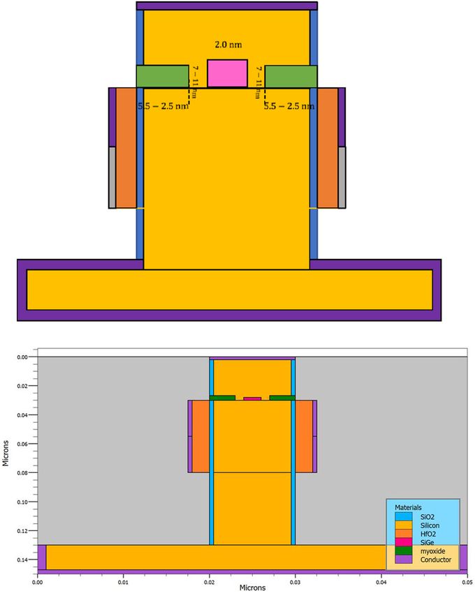
Figure 1(a) reflects the equivalent diagram of charge plasma              In the charge-plasma-based device, the virtual source
based SiGe heterojunction Vertical TFET structure. Figure 1           and virtual drain region are created by attaching suitable
(b) Simulated contour diagram of the proposed device via              work functions to gate electrodes VTFET. Platinum metal
silvaco TCAD tool. For employing parameter of intrinsic car-          electrode work function 5.93 eV is used to create the “p+”
rier concentration with the value of ni = 1.0 × 1015 cm−3 with        type source in the intrinsic silicon semiconductor.
non-metallurgical junctions. The device thickness is of 10 nm         Similarly, the hafnium work function 3.90 eV is used to
while the channel length is 50 nm. This device is opted the           create the “n+” type for the drain region in the device. In
gate stacking method with the specification 3 nm as a high-K          all above drafting of the proposed device one thing need
(HfO2) material with 0.55 nm as (SiO2) material. Based on the         to be acknowledge that the device thickness must be be-
findings, researchers looked into a comparison of low                 low the Debye length as express by the given Eq. (1) [19].

Fig. 1 (a) Schematic diagram (b)                (a)
Simulated Contour diagram of
Dual Modulated Charge plasma
                                                                                     Source(ϕ = 5.93 eV)
based SiGe Vertical TFET for                           t SiO 2 =0.5
biomolecules sensing

                                                                               My oxide            SiGe                 My Oxide    Biomolecule Cavity
                                                         Biomolecule Cavity
                                                                                                        1 × 1015 cm−3

                                                                                                                                   HfO2
                                                                        HfO2

                                                                                              Channel

                                                                                                                                                         SiO2
                                                                                                                                                         My oxide
                                                                                                                                                         Silicon
                                                                                                                                                         Conductor
                                                                                                                                                         HfO2
                                                      t HfO 2 = 3                                                                                        SiGe

                                                                                          Drain (φd= 3.90 eV)

                                               (b)
Silicon

                       1=2                                             simulation results, silvaco TCAD simulation software is used
    ðεsi V T Þ                                                           to carry for the validation off proposed device. The model
               þ 60:N                                             ð1Þ
        q                                                                used for simulating the device are Lombardi model,
                                                                         Shockley Read Hall (SRH) model for re-combination purpose
Where, VT represent the thermal voltage, εsi represent the               with Fermi -Dirac statistics with non-local band to band
dielectric constant, q and N terms represents the electronic             tunneling [31, 32]. The generation rate at the tunneling junc-
charge carrier and Silicon carrier concentration of the                  tion is also calculated using the nonlocal band-2-band tunnel-
device.                                                                  ing (BTBT) model. The device basically senses the biomole-
    The energy bandgap, electron affinity and permittivity of            cule by analyzing the variation of dielectric constant (K > 1)
SiGe material can be intended using following Eqs. (2 and 3).            with reference to the air dielectric constant (K > 1). Whenever
                                                                        the biomolecules come in contact with the cavity, the gate
           1:17−0:47x þ 0:24x2     x < 0:85
E SiGe ¼                                                  ð2Þ            capacitance increases, resulting in an increase in the drive
            5:88−9:58x þ 4:43x2 x > 0:85
                                                                         current of the vertical TFET based on charge plasma tech-
εSiGe ¼ 11:9ð1 þ 0:35xÞ                                           ð3Þ    nique, making it suitable for biomolecule sensing.
                                                                         Calibration Fig. 2 shows the calibration of doping less
Where, x is the mole fraction representing the variation from 0
to 1 in Si1-xGex. Schematic diagram of charge plasma based               Vertical TFET simulation using the testified work at Vds
                                                                         1.0 V. The data were extracted and plotted using the plot
SiGe vertical TFFT are identical to those for a conventional
                                                                         digitizer program.
device, with the exception that a cavity region is formed to
detect the biomolecule immobilization. Here, the channel is
separated into two regions, which are denoted by the label’s
region1 and region 2. The first region is basically the entrance
space of the biomolecule called as cavity also as gate under lap
                                                                         3 Results and Discussion
region (region 1), whereas the gate overlap region is known to
                                                                         In the natural environment we have basically two types neutral
be region 2. Where, Lg represent the second region (region 2)
                                                                         and charged biomolecules. For the assessment of the drain
as a gate overlap region with the dimension of 43 and 40 nm.
                                                                         current characteristics different approach need to be taken
Lcavity is gate under cavity length, with values of 6 nm and
                                                                         for the neutral and changes biomolecules. As in the neutral
10 nm, and values of 3.9 eV and 4.5 eV for dual-metal gate
                                                                         biomolecules, we have to only focused and examine the di-
workfunctions ϕm1 and ϕm2, respectively. Various device de-
                                                                         electric constant; however, in the case of the charged biomol-
sign parameters of the device are mentioned in Table 1.
                                                                         ecules, both the dielectric constant and charge have to be
    Finally, tcavity describes the cavity thickness and taken to
                                                                         examined for drain current variation. As a result, when the
be 2/5 as height is to width ratio, which is also the gate
                                                                         neutral biomolecules are taken in to the account for the pro-
underlap. The spacer thickness is fixed at 3.0 nm and
                                                                         posed device of the Charge plasma based SiGe Vertical TFET
15.0 nm, respectively. The gate oxide thickness, tox, is gate
                                                                         in the underlap region for simulating the drain current charac-
stacked with the HfO2 and SiO2 with the thickness of 0.5–
                                                                         teristics. On the other hand, charged biomolecules for the
3 nm. When the Si substrate is unmasked and exposed to the
air, the SiO2 layer acts as an adhesive, binding the biomole-                                       10-5
cules together. The cavity region is attached with the biomol-                                      10-6
ecules which further act as a biosensor region. For typical                                         10-7
                                                                         Drain Current Ids (A/Pm)

                                                                                                    10-8
                                                                                                    10-9
Table 1      Device specification of charge plasma based SiGe vertical                              10-10
TFET                                                                                                10-11
                                                                                                    10-12
Parameters                                         Values specified
                                                                                                    10-13
                                                                                                    10-14
Cavity dimension (Cavity thickness)                From 6 to 10 nm
                                                                                                    10-15                 Conventional V-TFET[32]
Cavity height (Cavity width)                       From 2.5 to 5.5 nm
                                                                                                    10-16                 Vertical TFET (Simulation Work)
Applied Gate work function (ϕm1 and ϕm2)           3.9 eV and 4.5 eV
                                                                                                    10-17
Gate stacked high k oxide thickness (HfO2)         3 nm
                                                                                                    10-18
SiO2 gate oxide thickness                          0.5 nm                                                0.00   0.25   0.50    0.75     1.00    1.25        1.50

Channel length                                     50 nm                                                               Gate voltage Vgs (V)
Charge plasma doping                               1×1015 cm−3           Fig. 2 Calibration of doping less Vertical TFET simulation using the
Source/Drain length                                30 nm                 reported work at Vds 1.0 V and Vgs 1.5 V. The data were extracted
                                                                         and plotted using the plot digitizer program
Silicon

underlap region will account the dielectric as well as changed       (a) 10-7
biomolecules.
                                                                                               10-8                 Cavity length = 6nm
                                                                                                                    Vgs =1.5 V , Vds = 0.5 V
3.1 Effects of Biomolecules Charge and Dielectric                                              10-9
Constant on Drain Current

                                                                     Drain Current (A/µm)
                                                                                            10-10

                                                                                            10-11
In this section, we will analysis neutral biomolecules effect on
the drain current with the cavity length of 6 nm underlap                                   10-12                                                                       k=1
condition at Vds = 0.5 V and Vgs = 1.5 V shown by the                                                  -13                                                              k=2
                                                                                            10
Figs. 3(a) and 5(a) respectively. However, the Figs. 4(a) and                                                                                                           k=5
                                                                                            10-14                                                                       k=7
6(a) represent the division in the (Ids) drain drive current char-
                                                                                                                                                                        k=9
acteristics owing to the cavity length of the 10 nm at the Vds =                            10-15
                                                                                                                                                                        k=11
1.5 V and Vgs = 1.5 V respectively.                                                         10-16
   With the creation of cavities, the barrier width between the
                                                                                            10-17
channel’s conduction band and the source’s valence band                                                      0.0           0.2    0.4    0.6       0.8   1.0      1.2        1.4
widens, resulting in an extremely low likelihood of electron
                                                                                                                                        Gate Voltage (V)
tunneling. As a result, current conduction is poor in this sce-           (b)
nario. The device ON current grows with an increase in the
                                                                                                 10-7                   Cavity length = 6nm
underlap condition of the dielectric constant, as shown in Figs.
                                                                                                 10-8                   Vgs =1.5 V , Vds = 0.5 V
3(a), 4(a), 5(a) and 6(a) respectively.
   On the other hand, the OFF-current remains nearly steady             Drain Current (A/µm)     10-9
when the dielectric constant rises, resulting in increased band                                10-10
bending and width reduction. The electrical characteristics                                    10-11
drain current for the scenario where charged biomolecules                                                                                                       Nf = 0
                                                                                               10-12
are immobilized in the cavity region are shown in Figs. 3(a)                                                                                                    Nf = 1e7
                                                                                                        -13
and (b), 4(a) and (b), 5(a) and (b) and 6(a) and (b) respectively.                             10
                                                                                                                                                                Nf = 1e9
   When there are positively charged proteins, the ION current                                 10-14
                                                                                                                                                                Nf = 1e11
rises, and when there are negatively charged biomolecules in                                   10-15                                                            Nf = 1e12
the cavity, the IOFF current decreases. It happens due to im-                                  10-16
mobilization of different polarity charge in the cavity region
                                                                                               10-17
reduces the barrier width between the channel’s conduction                                                    0.0          0.2    0.4    0.6       0.8   1.0     1.2        1.4
band and the source’s valance band.                                                                                                     Gate Voltage (V)
   The cavity is occupied with the biomolecules with the val-                   (c)
ue of dielectric constant at K > 50, the model is found to be                                          10-7
ineffective. The dielectric constants of a few biomolecules are                                        10-8
                                                                                                                        Cavity length = 6nm
shown in Table 2. The conductivity of these biomolecules                                                                Vgs =1.5 V , Vds = 0.5 V
                                                                                                             -9
                                                                                                       10
must range initially from semi-conductor to insulator.
                                                                                Drain Current (A/µm)

                                                                                                       10-10
   In this study, a gate underlaps dielectric modulated VTFET
                                                                                                       10-11
has been constructed to incorporate the dielectric modulation
                                                                                                       10-12
(DM) technology for label-free electronic detection based on
                                                                                                       10-13
biomolecules such as aminopropyl triethoxysilane, Biotin,                                                                                                      Nf = 0
                                                                                                       10-14
protein, uricase, DNA, enzyme, and so on as sown in                                                                                                            Nf = -1e7
Table 2 with their different values [33–35]. For the change                                            10-15                                                   Nf = -1e9
                                                                                                       10-16                                                   Nf = -1e11
plasma based SiGe VTFET, we examined a gate underlap
                                                                                                                                                               Nf = -1e12
arrangement with the trap condition of the biomolecules.                                               10-17
   This paper basically deals with Charge plasma based SiGe                                            10-18
                                                                                                                  0.0       0.2   0.4    0.6       0.8   1.0     1.2        1.4
Vertical TFET in order to account the dielectric modulation
                                                                                                                                        Gate Voltage (V)
technique for detection of label free biomolecules like
aminopropyl triethoxysilane, Biotin, protein, uricase, DNA,          Fig. 3 Drain current variation under the condition of gate underlap (Cavity)
                                                                     with the fixed dimension of 6 nm width with the height of 5.5 nm at Vds
enzyme etc. For this proposed device, we will analysis the
                                                                     0.5 V and Vgs 1.5 V for (a) Different dielectric constant values (K = 1, 2,
underlap distribution of my oxide, in which basically the ox-        5, 7, 9, 11) (b) for the positive charge density biomolecules with the
ide region is uncovered because of interaction of the biomol-        variation from Nf = 0 to 1e12. (c) for the negative charge density
ecules with the given cavity.                                        biomolecules with the variation from Nf = 0 to -1e12
Silicon

       (a)                                                                                  ƒFig. 4   Drain current variation under the condition of gate underlap
                         -10                                                                  (Cavity) with the fixed dimension of 10 nm width with the height of
                       10             Cavity length = 10 nm
                                                                                              5.5 nm at Vds 0.5 V and Vgs 1.5 V for (a) Different dielectric constant
                                      Vgs =1.5 V , Vds = 0.5 V
                       10-11                                                                  values (K = 1, 2, 5, 7, 9, 11) (b) for the positive charge density
                                                                                              biomolecules with the variation from Nf = 0 to 1e12. (c) for the
Drain Current (A/µm)

                       10-12                                                                  negative charge density biomolecules with the variation from Nf = 0 to
                                                                                              -1e12
                       10-13

                       10-14
                                                                                   k=1
                       10-15                                                                  −1 × 1012 cm2. When the cavity is filled with positively
                                                                                   k=2
                                                                                   k=5
                                                                                              charged biomolecules, the ON-current increases; however,
                       10-16
                                                                                   k=7        when neutral biomolecules filled the cavity, the OFF-current
                       10-17                                                       k=9        remains nearly constant (dielectric constant K = 6).
                                                                                   k=11          With the condition shown in Figs. 3(c), 4(c), 5(c) and 6(c),
                       10-18
                                                                                              the device based on underlap charge plasma condition of SiGe
                       10-19
                               0.0       0.2    0.4     0.6      0.8   1.0   1.2      1.4
                                                                                              Vertical TFET exhibit conflicting behavior for drain current as
                                                       Gate Voltage (V)
                                                                                              negative charge density increases, resulting in drain current
   (b)                                                                                        deterioration. Figures 3 and 5 show that when the cavity
                       10-8                                                                   length is 6 nm, the drain current reaches its greatest value,
                       10-9          Cavity length = 10 nm                                    whereas at Figs. 4 and 6 when the cavity length is 10 nm,
                                     Vgs =1.5 V , Vds = 0.5 V                                 the drain current reaches its minimum value.
                       10-10
Drain Current (A/µm)

                       10-11
                                                                                              3.2 Effects of Geometrical Parameter Variation on
                       10-12                                                                  Device Performance
                       10-13
                                                                                              3.2.1 Variation in Cavity Length Has an Effect on Drain
                       10-14                                                 Nf = 0           Current
                       10-15                                                 Nf = 1e7
                                                                             Nf = 1e9         Now Figs. 7(a) and 7(b) shows the drain current fluctuation
                       10-16
                                                                             Nf = 1e11        with respect to the cavity length (Lcavity). The ON current
                       10-17
                                                                             Nf = 1e12        will be decreases as the cavity length will start increases from
                       10-18                                                                  6 to 10 nm keeping the gate width fixed with 50 nm. When
                               0.0       0.2    0.4     0.6      0.8   1.0   1.2      1.4
                                                                                              compared to drain current at Vds = 0:5 V, the foregoing
                                                       Gate Voltage (V)                       characteristics reveal that variance in drain current at Vds =
   (c)
                        1E-9                                                                  1.5 V is insignificant. The fact that charge plasma based SiGe
                                      Cavity length = 10 nm                                   Vertical TFET exhibit tunnelling principle, whereas conven-
                       1E-10
                                      Vgs =1.5 V , Vds = 0.5 V                                tional DM JLTFETs do not, explains the small fluctuation in
                       1E-11                                                                  drain current seen as a result of changing cavity length. The
Drain Current (A/µm)

                       1E-12                                                                  diffusion principle is followed by FET.
                       1E-13
                                                                                              3.2.2 Variation in Cavity Thickness Has an Effect on Drain
                       1E-14
                                                                                              Current
                       1E-15                                                 Nf = 0
                       1E-16
                                                                             Nf = -1e7        Figures 8(a), 8(b) demonstrates the drain current versus gate
                                                                             Nf = -1e9        bias for various cavity thickness (tcavity) values while keep-
                       1E-17
                                                                             Nf = -1e11       ing channel length at 50 nm. When Vds = 1.5 V is compared
                       1E-18                                                 Nf = -1e12       to Vds = 0.5 V, a slight change in drain current is noted. With
                       1E-19
                                                                                              the variation in tcavity (cavity thickness) grows from 2.5 to
                                0.0       0.2    0.4    0.6      0.8   1.0   1.2     1.4      5.5 nm, the variance in drain current with relation to Vgs
                                                       Gate Voltage (V)                       (gate-source) voltage decreases. Figure 8 demonstrates that
                                                                                              when the cavity thickness tcavity is 2.5 nm, the drain current
                                                                                              reaches its extreme value. The effect of changing the tcavity
    As demonstrated in Figs. 3 and 4, a remarkable fluctuation                                on the Ids vs Vgs features is seen in Fig. 8. Higher tunnelling
 in the drain current is achieved during Nf = 1 × 1012 cm2 to                                 barriers at source-channel interface due to introduce SiGe
Silicon

(a)                                                                                             ƒFig. 5   Drain current variation under the condition of gate underlap
                         10-5                                                                     (Cavity) with the fixed dimension of 6 nm width with the height of
                                        Cavity length = 6 nm                                      5.5 nm at Vds 1.5 V and Vgs 1.5 V for (a) Different dielectric constant
                         10-6           Vgs =1.5 V , Vds = 0.5 V                                  values (K = 1, 2, 5, 7, 9, 11) (b) for the positive charge density
                         10-7                                                                     biomolecules with the variation from Nf = 0 to 1e12. (c) for the
                                                                                                  negative charge density biomolecules with the variation from Nf = 0 to
 Drain Current (A/µm)

                         10-8
                         10-9
                                                                                                  -1e12
                        10-10
                        10-11
                        10-12                                                         k=1
                                                                                                  3.3 Variation in the DCS (Drain Current Sensitivity)
                        10-13
                                                                                      k=2         with Various Parameters
                        10-14                                                         k=5
                                                                                      k=7         The drain current sensitivity of biosensors can be used to
                        10-15
                                                                                      k=9         assess their performance: The drain current levels while the
                        10-16                                                         k = 11
                                                                                                  cavity is empty and filled with a dielectric material are repre-
                        10-17
                                  0.0       0.2    0.4    0.6      0.8   1.0   1.2       1.4      sented by the Drain Current Sensitivity factor ID and IbioD,
                                                         Gate Voltage (V)                         represent by Eq. (4) respectively. By variation of the different
(b)                                                                                               values of neutral biomolecules and dielectric constant with
                         10-6                                                                     charge density of biomolecules.
                                        Cavity length = 6 nm
                         10-7
                                        Vgs =1.5 V , Vds = 1.5 V
                         10-8                                                                                                             
                                                                                                                     ðI d −I Biod Þ
                         10-9                                                                     DCS ð%Þ ¼                                                          ð4Þ
 Drain Current (A/µm)

                                                                                                                                    *100
                                                                                                                           Id
                        10-10
                        10-11                                                                     Figure 9(a) and 9(b) reflect the drain current sensitivity in
                        10-12                                                                     terms of gate voltage variation for two cavity length of the
                        10-13                                                                     underlap region with 6 nm and 10 nm respectively.
                                                                                Nf = 0
                        10-14                                                   Nf = 1e7             Figure 10 (a) and (b) demonstrates drain current sensitivity
                        10-15                                                   Nf = 1e9          characteristics for Vds = 1.5 V at 6 nm cavity length and
                        10-16                                                   Nf = 1e11         10 nm cavity length for various dielectric constant for neutral
                        10-17                                                   Nf = 1e12         biomolecules with different charge densities. The biomole-
                        10-18                                                                     cules are trapped in the cavity when the dielectric constant
                                  0.0       0.2    0.4    0.6      0.8   1.0    1.2       1.4     of the cavity areas is gradually increased form air to the en-
                                                         Gate Voltage (V)                         hanced values i.e., K > 1. Form the figure it can be depicted
(c)                                                                                               that drain current sensitivity is proportionate with the value of
                        10-6
                        10-7            Cavity length = 6 nm                                      dielectric constant value. As can be predicted form the Fig. 9
                             -8
                                        Vgs =1.5 V , Vds = 1.5 V                                  (b) and 10(b) that, drain current sensitivity increases with the
                        10
                                                                                                  increase with the positive concentration of biomolecules. It
                        10-9
Drain Current (A/µm)

                                                                                                  also causes shift in the drain current and potential to show
                        10-10
                                                                                                  the effect of the drain current sensitivity of charge plasma
                        10-11
                                                                                                  based SiGe Heterojunction Vertical TFET as a proportionate
                        10-12                                                                     behavior to the predict the presence of biomolecules in the
                        10-13                                                                     cavity. Table 3 shows that the factor of Drain current sensitiv-
                                                                               Nf = 0
                        10-14                                                                     ity (DCS) that grows as propionate the channel width in-
                                                                               Nf = -1e7
                        10-15                                                  Nf = -1e9          creases However, long channel length devices have poor sens-
                        10-16                                                  Nf = -1e11         ing capability. For different dielectric constant value and
                        10-17                                                  Nf = -1e12         charge density levels, it is clear that a low gate bias results in
                        10-18
                                                                                                  a large improvement in drain current sensitivity.
                                  0.0       0.2    0.4    0.6      0.8   1.0   1.2       1.4
                                                         Gate Voltage (V)
                                                                                                  3.3.1 Variation in Cavity Length Has an Effect on Drain
                                                                                                  Current Sensitivity (DCS)
pocket layer which reduce the tunneling barrier for high
values of Vgs, which finally resulting in a drop in drain current                                 Now in Fig. 11(a) and 11(b) DCS varies with respect to the
as tcavity grows.                                                                                 drain-source voltage Vds = 0.5 and 1.5 V. However, the
Silicon

(a)                                                                                                             Table 2                           Biomolecule equivalent value to dielectric Constant
                         10-7

                         10-8            Cavity length = 10 nm                                                  Name of biomolecule                                                           Equivalent K value
                                         Vgs =1.5 V , Vds = 1.5 V
                         10-9
                                                                                                                Aminopropyl triethoxy-silane                                                  3.570
                         10-10
Drain Current (A/µm)

                                                                                                                Biotin                                                                        2.630
                         10-11                                                                                  Protein                                                                       2.500
                         10-12                                                                                  Uricase                                                                       1.540
                         10-13
                                                                                              k=1
                         10-14
                                                                                              k=2
                         10-15                                                                k=5               reader can see the small fluctuation in drain current sensitivity
                         10-16
                                                                                              k=7
                                                                                              k=9               when Lcavity changes. As can be analyses from the Fig. 11,
                         10-17                                                                k = 11            the DCS variation will increases with respect to gate source
                         10-18                                                                                  voltage. At the 10 nm cavity length the sensitivity reflects its
                                 0.0         0.2    0.4     0.6     0.8     1.0         1.2         1.4
                                                                                                                maximum value. In the fraction where cavity length is not
                                                           Gate Voltage (V)
                                                                                                                much affected to the drain current sensitivity due to the fact
(b) 10                        -7

                                          Cavity length = 10 nm
                          10-8
                                          Vgs =1.5 V , Vds = 1.5 V                                              (a)
                          10-9                                                                                                          10-9

                         10-10                                                                                                          10-10         Vgs =0.5 V , Vds = 1.5 V
Drain Current (A/µm)

                         10-11                                                                                  Drain Current (A/µm)    10-11
                           -12
                         10
                                                                                                                                        10-12
                           -13
                         10
                                                                                                                                        10-13
                         10-14                                                            Nf = 0
                                                                                          Nf = 1e7                                      10-14
                         10-15
                                                                                          Nf = 1e9
                         10-16                                                                                                          10-15
                                                                                          Nf = 1e11
                                                                                                                                                                                               Lcavity = 6
                         10-17                                                            Nf = 1e12                                     10-16
                                                                                                                                                                                               Lcavity = 7
                         10-18                                                                                                          10-17                                                  Lcavity = 8
                                   0.0       0.2    0.4      0.6     0.8      1.0         1.2         1.4
                                                                                                                                                                                               Lcavity = 9
                                                           Gate Voltage (V)                                                             10-18
                                                                                                                                                                                               Lcavity = 10
(c) 10                         -7
                                                                                                                                        10-19
                                          Cavity length = 10 nm                                                                                 0.0       0.2    0.4    0.6      0.8    1.0       1.2     1.4
                          10-8            Vgs =1.5 V , Vds = 1.5 V                                                                                                     Gate Voltage (V)
                                                                                                                (b)
                          10-9                                                                                                           10-7
 Drain Current (A/µ m)

                              -10
                         10                                                                                                              10-8         Vgs =1.5 V , Vds = 1.5 V
                              -11
                         10                                                                                                              10-9
                         10-12
                                                                                                                                        10-10
                                                                                                                 Drain Current (A/µm)

                         10-13
                                                                                                                                        10-11
                                                                                              Nf = 0
                         10-14
                                                                                              Nf = -1e7                                 10-12
                         10-15
                                                                                              Nf = -1e9                                 10-13
                         10-16                                                                Nf = -1e11
                                                                                                                                        10-14                                           Lcavity = 6 nm
                         10-17                                                                Nf = -1e12
                                                                                                                                        10-15                                           Lcavity = 7 nm
                         10-18
                                    0.0       0.2    0.4      0.6     0.8         1.0         1.2         1.4
                                                                                                                                                                                        Lcavity = 8 nm
                                                                                                                                        10-16                                           Lcavity = 9 nm
                                                            Gate Voltage (V)
                                                                                                                                        10-17                                           Lcavity = 10 nm
Fig. 6 Drain current variation under the condition of gate underlap
(Cavity) with the fixed dimension of 10 nm width with the height of                                                                     10-18
5.5 nm at Vds 1.5 V and Vgs 1.5 V for (a) Different dielectric constant                                                                         0.0       0.2    0.4    0.6      0.8    1.0       1.2     1.4
values (K = 1, 2, 5, 7, 9, 11) (b) for the positive charge density                                                                                                     Gate Voltage (V)
biomolecules with the variation from Nf = 0 to 1e12. (c) for the
                                                                                                                Fig. 7 Variation of drain current characteristics with respect to the cavity
negative charge density biomolecules with the variation from Nf = 0 to
                                                                                                                length variation form the 6 nm to 10 nm for the gate source voltage Vgs
-1e12
                                                                                                                = 1.5 V (a) Vds = 0.5 V and (b) Vds = 1.5 V
Silicon

   (a)                                                                                       (a)
                       10-9                                                                                               104
                                        Vgs =0.5 V , Vds = 1.5 V                                                                       K=2      Cavity length = 6nm
                       10-10                                                                                                                    Vgs =1.5 V , Vds = 0.5 V
                                                                                                                                       K=5
                       10-11                                                                                                           K=7

                                                                                              Drain Current Senstivity
                       10-12                                                                                                           K=9
Drain Current (A/µm)

                                                                                                                          103          K=11
                       10-13

                       10-14

                       10-15

                       10-16
                                                                                                                          102
                       10   -17                                          tcavity = 2.5 nm
                                                                         tcavity = 3.5 nm
                       10-18
                                                                         tcavity = 4.5 nm
                       10-19                                             tcavity = 5.5 nm
                       10-20                                                                                              101
                                  0.0       0.2    0.4    0.6      0.8   1.0    1.2    1.4                                      0.0   0.2     0.4    0.6     0.8     1.0     1.2       1.4
                                                         Gate Voltage (V)                                                                           Gate Voltage (V)
   (b)                                                                                       (b)
                                                                                                                          104
                       10    -7                                                                                                   Cavity length = 6nm
                                        Vgs =1.5 V , Vds = 1.5 V
                       10    -8                                                                                                   Vgs =1.5 V , Vds = 0.5 V
                       10-9
                       10-10
                                                                                              Drain Current Sensitivity   103
Drain Current (A/µm)

                       10-11
                       10-12
                       10-13                                                                                              102
                         -14
                       10
                       10-15                                                                                                                                               Nf = 1e7
                       10-16                                                                                                                                               Nf = 1e9
                                                                         tcavity = 2.5 nm                                 101

                       10-17                                             tcavity = 3.5 nm                                                                                  Nf = 1e11
                       10-18                                             tcavity = 4.5 nm                                                                                  Nf = 1e12
                       10-19                                             tcavity = 5.5 nm
                                                                                                                          100
                       10-20
                                                                                                                                0.0   0.2     0.4    0.6     0.8     1.0     1.2       1.4
                                  0.0       0.2    0.4    0.6      0.8   1.0    1.2    1.4
                                                                                                                                                    GateVoltage (V)
                                                         Gate Voltage (V)
                                                                                             Fig. 9 Drain current sensitivity variation of Charge plasma based SiGe
Fig. 8 Variation of drain current characteristics with respect to the cavity
                                                                                             Vertical TFET with respect to the cavity gate voltage (V) fixed at 6 nm
thickness variation form the 2.5 nm to 5.5 nm for the gate source voltage
                                                                                             width with the height of 5.5 nm at Vds 0.5 V and Vgs 1.5 V for (a)
Vgs = 1.5 V (a) Vds = 0.5 V and (b) Vds = 1.5 V
                                                                                             Different dielectric constant values (K = 1, 2, 5, 7, 9, 11) (b) for the
                                                                                             positive charge density biomolecules with the variation from Nf = 0 to
                                                                                             1e12
that charge plasma-based Pocket SiGe Vertical TFET is basi-
cally using the tunneling mechanism, however in the case of
the conventional FET, diffusion process is used for the chan-                                voltage decreases. In the case of the cavity thickness at
nel transmission. As can be seen from Table 4, variation of                                  2.5 nm, the drain current sensitivity shows the maximum
drain current sensitivity with respect to cavity length variation                            value, however in the case of 5.5 nm cavity thickness in
is recorded. The DCS value is raises with the cavity length and                              DCS shows the minimum values. The drain current sen-
shown to be maximum at Lcavity = 10 nm.                                                      sitivity diminishes as the cavity length (tcavity) in-
                                                                                             creases, which is due to an increase in the tunneling
3.3.2 The Influence of Cavity Thickness (Tcavity) on DCS                                     barrier at the source-channel boundary, resulting in the
                                                                                             less sensing of the proposed device charge plasma based
Figure 12(a) and 12(b) demonstrate the drain current sensitiv-                               SiGe heterojunction Vertical TFET. As can be seen from
ity variation (DCS) as a function of cavity thickness tcavity for                            Table 5, variation of drain current sensitivity with respect
Vds 0.5 V and 1.5 V respectively. It shows that, when the                                    to cavity thickness variation is recorded. The DCS value
tcavity (cavity thickness) grows from 2.50 nm to                                             is raises with the cavity thickness and shown to be max-
5.50 nm, the DCS voltage with respect to the gate                                            imum at tcavity = 5.5 nm.
Silicon

Table 3 Variations of drain
current sensitivity with respect to                              Dielectric constant           DCS (Drain Current Sensitivity)
dielectric constant and positive
biomolecules                                                                                   Vds=0.5 V                                      Vds=1.5 V

                                                                                               Cavity (6 nm)         Cavity (10 nm)           Cavity (6 nm)       Cavity (10 nm)

                                                                 K=2                             80.46586             119.9166                   112.06047         163.46123
                                                                 K=5                            529.33125             888.17709                  368.39524         600.43308
                                                                 K=7                           1419.89688            2132.34902                1295.99963         1349.28134
                                                                 K=9                           3274.52697            4673.52129                4692.57192         2943.90593
                                                                 K=11                          7645.38766            9685.62485               10,723.00076        6259.3497

                                                                                                           4 Conclusion
(a)                                                                                                        In this paper, we have basically analysis the charged
                                 104                                Cavity length = 10 nm                  and neutral biomolecule detection with the proposed de-
                                                                    Vgs =1.5 V , Vds = 0.5 V               vice of charge plasma based SiGe heterojunction
                                                                                                           Vertical TFET for under lap region. This draft makes
 Drain Current Sensitivity

                                 103                                                                       its own space to the readers by distinguishes it from
                                                                                                           other sensing devices currently on the commercial ap-
                                                                                                           plication for showing its maximum sensitivity in detec-
                                 102                                                                       tion of the charge and neutral biomolecules. So, the
                                                                                                           proposed device reflects its improved performance for
                                                                                                           cost-effective construction of biomedical diagnosis in-
                                 101                Nf = 1e12                                              struments, as it achieves increased sensitivity by a mod-
                                                    Nf = 1e11                                              erate optimum selection to the geometrical parameters
                                                    Nf = 1e9                                               like cavity length and its thickness at the tunneling
                                 100                Nf = 1e7                                               junction interface with suitable biasing condition. The
                                             0.2    0.4    0.6      0.8     1.0        1.2     1.4         biasing voltage Vgs is kept ot be 1.5 V, while the
                                                          Gate Voltage (V)                                 Vds is varied from 0.5 to 1.5 V. Finally, form the
(b)                                                                                                        proposed device of charge plasma based SiGe vertical
                                 104                                                                       TFET it can be concluded that, it is a low leakage
                                         Cavity length = 10 nm                                             device current and highly sensitive factor for the change
                                         Vgs =1.5 V , Vds = 0.5 V
                                                                                                           and neutral biomolecules, after analyzing its variation to
     Drain Current Sensitivity

                                 103                                                                       different cavity dimension parameters with dielectric
                                                                                                           constant to its electrical characteristics.

                                 102

                                                                                        K=2
                                                                                        K=5                Table 4 Variations of drain current sensitivity (DCS) with respect to
                                   1
                                 10                                                     K=7                cavity length variation
                                                                                        K=9
                                                                                                           Lcavity (nm)          Maximum DCS (Drain Current Sensitivity)
                                                                                        K=11
                                 100                                                                                             At K=5
                                       0.0   0.2    0.4    0.6      0.8     1.0        1.2     1.4
                                                          Gate Voltage (V)                                                       Vds=0.5 V                    Vds=1.5 V

Fig. 10 Drain current sensitivity variation of Charge plasma based SiGe                                    7                        112.060                   1688.2
Vertical TFET with respect to the cavity gate voltage (V) fixed at 10 nm
                                                                                                           8                        368.395                    496.09
width with the height of 5.5 nm at Vds 0.5 V and Vgs 1.5 V for (a)
Different dielectric constant values (K = 1, 2, 5, 7, 9, 11) (b) for the                                   9                      1295.996                     197.74
positive charge density biomolecules with the variation from Nf = 0 to                                     10                    10,723.0                       39.68
1e12
Silicon

(a)                                                                                                                   (a)
                                               Vgs =1.5 V , Vds = 0.5 V                                                                                      tcavity = 2.5 nm    Cavity length = 6 nm
                              104                                                                                                                            tcavity = 3.5 nm    Vgs =1.5 V , Vds = 0.5 V
                                                                                                                                           104
                                                                                                                                                             tcavity = 4.5 nm
Drain Current Sensitivity

                                                                                                            Drain Current Sensitivity
                                                                                                                                                             tcavity = 5.5 nm
                              103

                              102                                                                                                          103

                                                                                           Lcavity = 6
                                                                                           Lcavity = 7
                              101                                                          Lcavity = 8
                                                                                           Lcavity = 9
                                                                                           Lcavity = 10                                    102

                                           0.0      0.2      0.4      0.6    0.8    1.0        1.2    1.4                                                   0.2    0.4    0.6    0.8    1.0      1.2     1.4
                                                                   Gate Voltage (V)                                                                                      Gate Voltage (V)
(b)                                        5
                                                                                                                      (b)
                                         10
                                                                                                                                                                                  Cavity length = 6nm
                                                                            Vgs =1.5 V , Vds = 1.5 V                                                    4                         Vgs =1.5 V , Vds = 1.5 V
                                                                                                                                                      10

                                                                                                                          Drain Current Sensitivity
             Drain Current Sensitivity

                                         104

                                                                                                                                                      103

                                         103
                                                                                                                                                      102

                                                          Lcavity = 7
                                         102              Lcavity = 8                                                                                                                       tcavity = 2.5 nm
                                                          Lcavity = 9                                                                                 101                                   tcavity = 3.5 nm
                                                          Lcavity = 10                                                                                                                      tcavity = 4.5 nm
                                                                                                                                                                                            tcavity = 5.5 nm

                                                    0.2      0.4      0.6     0.8    1.0       1.2    1.4                                                    0.2   0.4    0.6    0.8    1.0      1.2    1.4

                                                                     Gate Voltage (V)                                                                                    Gate Voltage (V)

Fig. 11 Drain current sensitivity variation of Charge plasma based SiGe                                     Fig. 12 Drain current sensitivity variation of Charge plasma based SiGe
Vertical TFET with different values of cavity length variation form 6 nm                                    Vertical TFET with different values of cavity thickness variation form
to 10 nm at Vgs 1.5 V for (a) Vds = 0.5 V and (b) Vds = 1.5 V                                               2.5 nm to 5.5 nm at Vgs 1.5 V for (a) Vds = 0.5 V and (b) Vds = 1.5 V

                                                                                                            Acknowledgements Not Applicable.

                                                                                                            Funding Statement The author(s) received no financial support for the
                                                                                                            research, authorship, and/or publication of this article.
Table 5 Variations of drain current sensitivity (DCS) with respect to
cavity thickness variation                                                                                  Availability of Data and Material Not applicable.

tcavity (nm)                                              Maximum DCS (Drain Current Sensitivity)           Author Contributions All authors have equally participated in the prepar-
                                                                                                            ing of the manuscript during implementation of ideas, findings result, and
                                                          At K=5                                            writing of the manuscript.
                                                          Vds=0.5 V                     Vds=1.5 V
                                                                                                            Data Availability Not applicable.
2.5                                                        163.461                      2772.2
3.5                                                        600.433                       857.394            Declarations       All procedures performed in studies involving human
4.5                                                       1349.281                       218.56             participants were in accordance with the ethical standards.
5.5                                                       2943.90                         36.062
                                                                                                            Consent to Participate Not applicable.
Silicon

Consent for Publication     The Author transfers his copyrights to the         18.   Wadhwa G, Kamboj P, Raj B (2019) Design optimisation of
publisher.                                                                           junctionless TFET biosensor for high sensitivity. Adv Nat Sci
                                                                                     Nanosci Nanotechnol 10(4):045001
Conflict of Interest The authors declare that there are no conflicts of        19.   Bala S, Khosla M (2018) Design and analysis of electrostatic doped
interest.                                                                            tunnel CNTFET for various process parameters variation.
                                                                                     Superlattice Microst 124:160–167
                                                                               20.   Gupta, Shilpi, Subodh Wairya, and Shailendra Singh (2021)
                                                                                     Analytical modeling and simulation of a triple metal vertical
References                                                                           TFET with hetero-junction gate stack. Superlattice Microst:
                                                                                     106992.
 1.   Tanaka J, Toyabe T, Ihara S, Kimura S’i, Noda H, Itoh K (1993)           21.   Wadhera T, Kakkar D, Wadhwa G, Raj B (2019) Recent advances
      Simulation of sub-0.1-mu m MOSFETs with completely sup-                        and progress in development of the field effect transistor biosensor:
      pressed short-channel effect. IEEE Electron Device Lett 14(8):                 a review. J Electron Mater 48(12):7635–7646
      396–399                                                                  22.   Bala S, Khosla M (2018) Design and simulation of nanoscale
 2.   Bricout P-H, Dubois E (1996) Short-channel effect immunity and                 double-gate TFET/tunnel CNTFET. J Semicond 39(4):044001
      current capability of sub-0.1-micron MOSFET's using a recessed           23.   Bala S, Khosla M (2019) Design and performance analysis of low-
      channel. IEEE Trans Electron Devices 43(8):1251–1255                           power SRAM based on electrostatically doped tunnel CNTFETs. J
 3.   Singh, Shailendra, and Balwinder Raj (2018) Vertical tunnel-fet                Comput Electron 18(3):856–863
      analysis for excessive low power digital applications. In: 2018 first    24.   Peesa, Rohit Bhargav, and Deepak Kumar Panda (2021) Rapid
      international conference on secure cyber computing and communi-                detection of biomolecules in a junction less tunnel field-effect tran-
      cation (ICSCCC). IEEE, pp. 192–197.                                            sistor (JL-TFET) biosensor. Silicon: 1–7
 4.   Shockley W (1984) The path to the conception of the junction             25.   Singh S, Raj B (2020) Analytical modeling and simulation analysis
      transistor. IEEE Trans Electron Devices 31(11):1523–1546                       of T-shaped III–V heterojunction vertical T-FET. Superlattice
                                                                                     Microst 147:106717
 5.   Singh, Shailendra, and Balwinder Raj (2020) Study of parametric
                                                                               26.   Aslam M, Sharma D, Yadav S, Soni D, Sharma N, Gedam A (2019)
      variations on hetero-junction vertical t-shape TFET for suppressing
                                                                                     A comparative investigation of low work-function metal implanta-
      ambipolar conduction.
                                                                                     tion in the oxide region for improving electrostatic characteristics of
 6.   Singh, Shailendra, and Balwinder Raj (2021) Analytical and com-
                                                                                     charge plasma TFET. Micro Nano Lett 14(2):123–128
      pact modeling analysis of a SiGe hetero-material vertical L-shaped
                                                                               27.   Devi WV, Bhowmick B, Pukhrambam PD (2020) N+ pocket-
      TFET. Silicon: 1–11
                                                                                     doped vertical TFET for enhanced sensitivity in biosensing appli-
 7.   Moore, Gordon E (1965) Cramming more components onto inte-                     cations: modeling and simulation. IEEE Trans Electron Devices 67
      grated circuits: 114–117.                                                      (5):2133–2139
 8.   Frank DJ, Dennard RH, Nowak E, Solomon PM, Taur Y, Wong H-               28.   Wangkheirakpam VD, Bhowmick B, Pukhrambam PD (2020) N+
      SP (2001) Device scaling limits of Si MOSFETs and their applica-               pocket doped vertical TFET based dielectric-modulated biosensor
      tion dependencies. Proc IEEE 89(3):259–288                                     considering non-ideal hybridization issue: a simulation study. IEEE
 9.   Roy K, Mukhopadhyay S, Mahmoodi-Meimand H (2003) Leakage                       Trans Nanotechnol 19:156–162
      current mechanisms and leakage reduction techniques in deep-             29.   Singh, Shailendra, Shilpi Yadav, and Sanjeev Kumar Bhalla (2021)
      submicrometer CMOS circuits. Proc IEEE 91(2):305–327                           An improved analytical modeling and simulation of gate stacked
10.   Singh S, Raj B (2020) Modeling and simulation analysis of SiGe                 linearly graded work function vertical TFET. Silicon: 1–14
      heterojunction double gate vertical t-shaped tunnel FET.                 30.   Wang P-F, Hilsenbeck K, Nirschl T, Oswald M, Stepper C, Weis
      Superlattice Microst 142:106496                                                M, Schmitt-Landsiedel D, Hansch W (2004) Complementary
11.   Edgar, Lilienfeld Julius. Method and apparatus for controlling elec-           tunneling transistor for low power application. Solid State
      tric currents. U.S. Patent 1,745,175, issued January 28, 1930                  Electron 48(12):2281–2286
12.   Singh S, Raj B (2020) Two-dimensional analytical modeling of the         31.   Manual, ATLAS User’S (2008) Device simulation software.
      surface potential and drain current of a double-gate vertical t-shaped         Silvaco Int., Santa Clara, CA
      tunnel field-effect transistor. J Comput Electron 19(3):1154–1163        32.   Nigam K, Kondekar P, Sharma D (2016) High frequency perfor-
13.   Rabaey, Jan M., Anantha P. Chandrakasan, and Borivoje Nikolic                  mance of dual metal gate vertical tunnel field effect transistor based
      (2003) The devices. In: Digital integrated circuits: a design perspec-         on work function engineering. Micro Nano Lett 11(6):319–322
      tive, 2nd edn. Pearson Education, New York.                              33.   Wadhera T, Kakkar D (2020) Conditional entropy approach to
14.   Singh S, Raj B (2019) Design and analysis of a heterojunction                  analyze cognitive dynamics in autism spectrum disorder. Neurol
      vertical t-shaped tunnel field effect transistor. J Electron Mater 48          Res 42(10):869–878
      (10):6253–6260                                                           34.   Wadhera T, Kakkar D (2021) Social cognition and functional brain
15.   Dennard, R. H., F. H. Gaensslen, L. Kuhn, and H. N. Yu (1972)                  network in autism spectrum disorder: insights from EEG graph-
      Design of micron MOS switching devices, IEDM. Dig Techn Pap:                   theoretic measures. Biomed Signal Process Control 67:102556
      344                                                                      35.   Verma SK, Singh S, Wadhwa G, Raj B (2020) Detection of bio-
16.   Singh S, Khosla M, Wadhwa G, Raj B (2021) Design and analysis                  molecules using charge-plasma based gate underlap dielectric mod-
      of double-gate junctionless vertical TFET for gas sensing applica-             ulated Dopingless TFET. Trans Electr Electron Mater 21(5):528–
      tions. Appl Phys A 127(1):1–7                                                  535
17.   Singh S, Raj B (2021) Analytical modelling and simulation of Si-
      Ge hetero-junction dual material gate vertical T-shaped tunnel FET.      Publisher’s Note Springer Nature remains neutral with regard to jurisdic-
      Silicon 13:1139–1150                                                     tional claims in published maps and institutional affiliations.
You can also read