Fabrication of solderable intense pulsed light sintered hybrid copper for flexible conductive electrodes - Nature
←
→
Page content transcription
If your browser does not render page correctly, please read the page content below
www.nature.com/scientificreports
OPEN Fabrication of solderable intense
pulsed light sintered hybrid copper
for flexible conductive electrodes
Yong‑Rae Jang1, Robin Jeong2, Hak‑Sung Kim 1,3*
& Simon S. Park 2*
Additively printed circuits provide advantages in reduced waste, rapid prototyping, and versatile
flexible substrate choices relative to conventional circuit printing. Copper (Cu) based inks along with
intense pulsed light (IPL) sintering can be used in additive circuit printing. However, IPL sintered
Cu typically suffer from poor solderability due to high roughness and porosity. To address this,
hybrid Cu ink which consists of Cu precursor/nanoparticle was formulated to seed Cu species and
fill voids in the sintered structure. Nickel (Ni) electroplating was utilized to further improve surface
solderability. Simulations were performed at various electroplating conditions and Cu cathode surface
roughness using the multi-physics finite element method. By utilizing a mask during IPL sintering,
conductivity was induced in exposed regions; this was utilized to achieve selective Ni-electroplating.
Surface morphology and cross section analysis of the electrodes were observed through scanning
electron microscopy and a 3D optical profilometer. Energy dispersive X-ray spectroscopy analysis
was conducted to investigate changes in surface compositions. ASTM D3359 adhesion testing was
performed to examine the adhesion between the electrode and substrate. Solder-electrode shear tests
were investigated with a tensile tester to observe the shear strength between solder and electrodes.
By utilizing Cu precursors and novel multifaceted approach of IPL sintering, a robust and solderable Ni
electroplated conductive Cu printed electrode was achieved.
Recent advancements in flexible electronics have made way for exciting developments in devices such as: radio
frequency identification (RFID) t ags1,2, flexible d
isplays3–5, flexible organic light-emitting diode (OLED)6,7, flex-
8,9 10,11
ible solar cells , and wearable electronics . This is possible through use of flexible polymer-based substrates
that can accommodate large deformations without sustaining structural damage. Utilizing common polymers
as substrates such as polyimide (PI), polyethylene terephthalate (PET), and polyethylene terephthalate glycol
(PETG) provide a pathway to a wide variety of robust and cheap electronic devices. However, these polymers are
susceptible to damage from high temperature processes due to their low glass-transition temperatures ranging
as low as 67 °C. As a result, modern high-temperature photolithography processes can be incompatible with
flexible polymers without additional processing.
Alternatively, printing and IPL-sintering loose conductive nanoparticles can produce highly conductive tracks
without thermal damage to the substrate. This low-temperature process can be streamlined to just three stages:
printing-sintering-diagnosis. Metallic nanoparticles (NPs) are of interest in printed electronics due to their high
electrical conductivity and simple ink-phase synthesis which can be readily implemented into existing print-
ing technologies such as inkjet. Sintering via IPL bypasses high temperature processing by using the surface
plasmonic effect; during IPL irradiation, electrons on the surface of nanomaterials resonate at a frequency that
collapses its surface energy and allows significant necking/densification within the loose particles12–14. This effect
significantly reduces sintering temperature and time requirements, which would otherwise damage the flexible
substrate and immensely increase the manufacturing cost of flexible electronics. Due to the high surface area to
volume ratio inherent in NPs, oxidation of metals is a large concern. Thus, noble and highly conductive metallic
NPs such as gold (Au) and silver (Ag) are often used; however, these precious metals are prohibitively expensive,
and their cost is further increased when processed into nanoparticle form. Copper (Cu) NPs are a lower cost
option that still provides excellent electrical conductivity. To utilize Cu-based inks, Cu’s inherent susceptibility
to oxidation must be addressed. IPL sintering has previously been utilized to reduce the Cu oxide shells by heat
1
Department of Mechanical Engineering, Hanyang University, 222, Wangsimni‑ro, Seongdong‑gu, Seoul 04763,
Republic of Korea. 2Department of Mechanical and Manufacturing Engineering, Schulich School of Engineering,
University of Calgary, 2500 University Drive NW, Calgary, AB T2N 1N4, Canada. 3Institute of Nano Science and
Technology, Hanyang University, 222, Wangsimni‑ro, Seongdong‑gu, Seoul 04763, Republic of Korea. *email:
kima@hanyang.ac.kr; simon.park@ucalgary.ca
Scientific Reports | (2021) 11:14551 | https://doi.org/10.1038/s41598-021-94024-8 1
Vol.:(0123456789)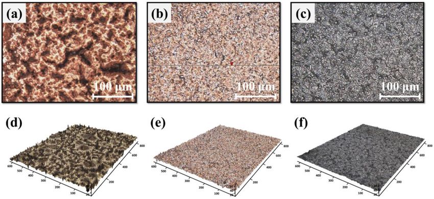
www.nature.com/scientificreports/
generation from surface plasmonic resonance and photo-degradation of polymeric b inders15. IPL thus provides
electrically conductive and oxide species reduction that reduce Cu particles for a high-performance ink receptive
of existing printing t echnologies16–18.
Challenges still occur with IPL sintered Cu-inks in regard to their porosity, surface roughness, and mechani-
cal strength. High porosity and surface roughness are of concern as it adversely affects solderability and thus
inhibits integration with modern flexible printed circuit board (FPCB) manufacturing. Salam et al.19 confirmed
that the poor solderability of printed Cu is due to its surface roughness and heterogeneity (mix of Cu and
voids). In addition, polymeric binders are typically introduced to reduce copper oxides during IPL sintering. As
polymeric binders thermally decompose, they leave behind pores which further increase the porosity issue of
sintered nanoparticles20. Conventional sintering in powder metallurgy is done on previously pressed (‘green’)
parts. These parts have already been compacted under high pressures which minimizes issues in final density
and surface features. Compaction of printed-inks under high pressures, however, this adds further complexities
and may damage the polymeric substrates. For these reasons, it has been difficult to realize the mass production
of ink-printed electronic circuit components.
Electroplating is one method that can reduce surface roughness. Nickel (Ni) electroplating is an ideal candi-
date to provide a smooth, scratch-resistant, surface. A homogenous Ni surface facilitates good solderability while
providing high mechanical strength without compromising electrical conductivity and oxidation susceptibility.
Thus, a Ni plated printed Cu circuit produces a conductive, solderable (smooth surface), oxidation resistant, and
mechanically resilient electrode21–24. However, Ni-electroplating deposition is limited to the surface and does not
address internal porosity which can impair conductivity and adhesion to the polymeric substrate; in-addition, Ni
deposition suffers from a lack of selectivity when presented with a conductive copper surface and is challenging
to produce a desired circuit pattern. To address this, the initial non-conductive nature of unsintered inks can be
utilized to form conductive and nonconductive patterns with selective exposure of IPL. By using a simple mask,
an electrically conductive copper pattern is produced after IPL sintering; these patterns, specific to the electronic
device or electrode requirements are sites of Ni electro-deposition while the non-conductive non-sintered regions
do not participate in electroplating. This simple and selective plating of only IPL sintered tracks can be utilized
to incorporate electroplating to the production of ink-based circuitry with minimal complexity.
In this study, solderability of printed and sintered Cu surfaces has been investigated by reducing internal
porosity and surface roughness. To reduce internal porosity and surface roughness, Cu is seeded on Cu NPs.
Chung et al.25 found that Cu precursors (Cu (II) nitrate trihydrate, Cu(NO3)2) exposed to IPL irradiation ther-
mally degrade and precipitate as Cu (I) oxide. By introducing polyvinylpyrrolidone (PVP), these oxide Cu seeds
are thermally degraded during IPL sintering to produce a dense and smooth Cu electrode. In addition, IPL is
utilized to produce a circuit pattern that is selectively plated by Ni electroplating to enhance solderability and
mechanical strength. The present novel application of multifaceted IPL sintering is optimized through initial ink
composition as well as sintering and electroplating parameters. To assist in the parametric study of Ni electro-
plating, multi-physics FEM simulations were conducted; evolution of the Ni surface roughness as well as deposit
thickness at various current densities, plating times, and bath temperatures were noted during simulations and
experimentally verified.
The goal of the present work is to create a solderable electrode manufactured from printable Cu NP based
ink. By utilizing IPL sintering with Cu precursors followed by Ni electroplating, a robust smooth electrode was
produced. Experiments were performed to reveal additional characteristics of the present electrode production
process such as: resistivity of the Cu precursor/NP (CPN) electrode using the 4-probe method; and surface
morphology and cross-sectional analysis using both a 3D optical profiler and SEM after Ni electroplating of the
IPL sintered CPN electrodes. Solder shear tests and simulations were conducted to investigate the correlation
between the surface roughness and solderability. In addition, the contact angle of the solder was measured to
confirm the wettability of solder on each type of electrode. Selectivity tests were performed by exposing only half
of the printed electrode surface to flash-sintering. The half-electrodes were electroplated at optimal conditions
to observe selective plating of sintered portions. Based on these results, the process conditions for solderable IPL
sintered Cu electrodes were established for electrical circuit manufacturing by printed electronics technology.
Experiments
A Cu-based conductive ink was fabricated by mixing the Cu NPs and Cu precursors. The Cu precursor/NP
(CPN) ink was sintered with IPL irradiation followed by Ni electroplating (Fig. 1). Various properties of the
Ni-electroplated CPN electrode were characterized to explore their effects on solderability.
Fabrication of Cu NPs ink & Cu precursor/NPs (CPN) ink. For ink synthesis, poly(N-vinylpyrro-
lidone) (PVP, MW 55,000; Sigma Aldrich) (0.08 g) was dissolved in diethylene glycol (DEG, 99%; Sigma Aldrich)
(1.08 g) and ultra-sonicated for 1 h. For Cu NPs ink, only Cu NPs (diameter, 50 nm) (2.16 g) were added to the
PVP-DEG solution. For CPN ink, Cu NPs (diameter, 50 nm) (2.16 g), diethylene glycol butyl ether (DEGBE,
99%; Sigma Aldrich) (0.47 g), and the PVP-DEG complex solvent were vortexed for 1 min followed by 20 min
of ultra-sonication. Cu precursors (Cu(NO3)2, 30 wt.% of Cu NPs; Sigma Aldrich) (0.648 g) were dispersed in a
prepared solvent using an ultra-sonicator for 1 h (see Table 1).
The CPN inks were printed using the doctor blade method using 50 μm thick polyimide (PI) substrates as
5 mm × 50 mm long tracks. The printed CPN ink was dried at 90 °C for 10 min on a hot plate followed by drying
under vacuum for 12 h to completely remove residual solvents. IPL sintering was carried out with Xenon S-2300
Dual-Stage Sintering System with IPL irradiation conditions (pulse on-time, 3 ms; pulse number, 1; pulse energy,
3.04–5.88 J/cm2) to achieve a final sintered thickness of 25 μm. Samples prepared for selective electroplating
were masked with aluminium foil to expose only half of the printed electrodes to IPL. By utilizing a simple mask
Scientific Reports | (2021) 11:14551 | https://doi.org/10.1038/s41598-021-94024-8 2
Vol:.(1234567890)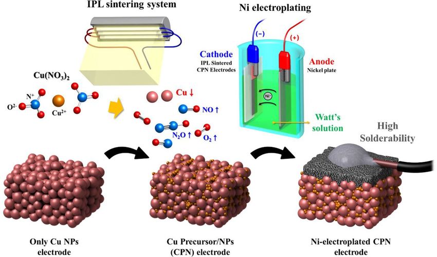
www.nature.com/scientificreports/
Figure 1. Highly solderable nickel electroplated Cu Precursor/NPs electrode.
Cu NPs ink
composition CPN ink compositions
PVP 0.08 g PVP 0.08 g
DEG 1.08 g DEG 1.08 g
Cu NPs 2.16 g DEGBE 0.47 g
Cu NPs 2.16 g
Cu(NO3)2 0.648 g (30 wt.% of Cu NPs)
Table 1. Material composition of Cu NPs ink and CPN ink.
Figure 2. Half-sintered CPN ink flexible electrodes sintered at 2800 V for 3 ms (5.17 J/cm2) for selective
electroplating investigations.
(demonstrated here with aluminium foil), electroplating can be incorporated to produce a conductive, solderable,
and mechanically robust printed circuit (Fig. 2).
Nickel electroplating of CPN electrodes. A Watt’s solution containing: nickel (II) chloride (NiCl2;
Sigma Aldrich) (40 g/L), nickel (II) sulfate (NiSO4; Sigma Aldrich) (250 g/L) and boric acid (H3BO3; Sigma
Aldrich) (45 g/L) was dispersed by sonicator for 24 h ours26,27 (Table 2). For better electrical conductivity, semi-
bright Watt’s solution was utilized. A nickel plate (2 cm × 8 cm), and IPL sintered CPN on the polymeric sub-
strate were wired as the anode and cathode, relatively. 2, 5, 10 A/dm2 current densities were applied using a DC
Scientific Reports | (2021) 11:14551 | https://doi.org/10.1038/s41598-021-94024-8 3
Vol.:(0123456789)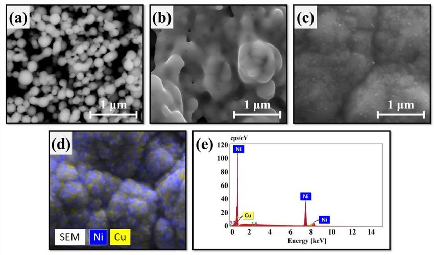
www.nature.com/scientificreports/
Bath composition Operating conditions
NiCl2 40 g/L Current density 2, 5, 10 A/dm2
NiSO4 250 g/L Time 1, 5, 10 min
H3BO3 45 g/L Bath Temp 40, 60 °C
pH 3.2
Electrode distance 1 cm
Table 2. Bath composition and operating conditions for semi-bright Watt’s solution Ni electroplating.
power supply (Model 9103; 42 V/ 20 A/ 320 W; BK Precision). In addition, for a smoother electroplated Ni layer,
plating time (1, 3, 5 min) and bath temperature (40, 60 °C) were controlled. During the electroplating process,
pH was fixed at 3.2 and the electrode distance between was fixed to 1 cm.
A total of 18 electroplating conditions were explored and the surface roughness, thickness, and adhesion of the
Ni layer on each electrode was measured. Surface roughness was measured using a 3D optical profiler (Zeta-20;
Zeta Instruments). The thickness of the Ni layer was obtained by measuring the thickness of the CPN electrode
prior to electroplating and then subtracted from the measured thickness after electroplating. For adhesion char-
acterization, values from 0 to 5B were obtained through an ASTM D 3359 adhesion test. Following the ASTM
D3359-B (the cross-cut tape test), each electrode was cut 6 times in both horizontal and vertical directions to
form a total of 25 grids with sizes of 2 mm × 2 mm. It was cut by applying sufficient force so that it can be cut
completely in the thickness direction of the electrode.
Characterizations. The electrical resistivity of IPL sintered Cu NP, CPN, and electroplated CPN electrodes
was obtained by converting the sheet resistance measured through the 4-point probe method. For Ni-electro-
plated CPN, the sheet resistance was measured in the form of a double layer in which a Ni layer was applied
on an uneven Cu electrode. Therefore, the resistivity was calculated after assuming the entire Ni-electroplated
CPN electrode as a metal alloy. The CPN electrode had a resistivity of 12.2 μΩ∙cm sintered under the optimum
IPL conditions (pulse on-time, 3 ms; IPL energy density, 5.13 J/cm2), and the resistivity of the entire electrode
considering each thickness of the Ni layer was calculated.
Among the 18 cases of Ni-electroplated CPN electrodes, the highest quality specimens (s-16) were used to
compare with Cu NP and CPN (non-plated) electrodes. 3D optical profiler (Zeta-20; Zeta Instrument) was uti-
lized to observe the surface roughness of each specimen. A root-mean-square deviation of surface topography
(Sq) was measured to compare surface roughness. The surface roughness analysis area was 831 μm × 623 μm with
200 height steps with a step size of 0.357 μm. Cross sectional analysis was performed to compare porosity and
electroplating deposit characteristics. Each specimen was immersed in liquid nitrogen, frozen, and then broken to
minimize deforming the cross-section of the specimen. The prepared specimens were subjected to SEM analysis
to visually compare the packing density of each electrode layer. In the case of Ni electroplated CPN electrode, the
distribution of surface components was identified through EDS analysis. To investigate the mechanical property
of the Ni-electroplated CPN electrode as a FPCB, adhesion testing was conducted based on ASTM D3359.
Soldering on the Ni‑electroplated CPN electrodes. Solder (Sn99-Ag-0.3-Cu0.7) was applied to test
the solderability of three different kinds of electrodes (i.e., Cu NPs electrode, CPN electrode, and Ni-electro-
plated CPN electrodes). The contact angle between the molten solder droplet and each type of electrode was
measured to compare the effect of surface roughness to solder wetting using a contact angle measurement sys-
tem (Smartdrop; Femtofab Co.).
In addition, shear strength between solder and the electrode was measured with a tensile tester (ESM303,
1.5 kN; Mark-10). Using solder wire and a soldering iron at 250 °C, a conductive wire was attached to the Ni-
electroplated CPN electrode. The shear tensile test was performed by fixing the wire and PI substrate to the tensile
tester after the solder was firmly hardened. The area between solder and electrode was kept to 20 mm2 in all cases,
and the test was conducted at a constant speed of 0.3 mm/min. The tensile test proceeded until the solder was
completely stripped from the electrode, and the recorded stress at failure was compared.
Through the above experiments, it was confirmed that the surface morphology of the electrodes is changed,
and the solderability is improved through addition of Cu precursors and Ni-electroplating.
Finite element method (FEM) simulation of Ni electroplating
Modelling for Ni electroplating on the CPN electrode and relationship between surface roughness and Ni-
electroplating parameters are presented in this section. Ni-deposit behaviour was studied using a multi-physics
FEM software by approximating the surface of the CPN electrode as a continuous row of triangles with fillets. To
achieve these simulations, the electrodeposition tool in Chemical Engineering Module was selected. The deposi-
tion of Nickel layer on the Cu electrode is one of the modeling methods of the electrodeposition process in multi-
physics FEM: ‘The standard model Copper Deposit in a Trench’. This simulation example is based on a research
by Mattsson et al.28; where a rough copper electrode surface was applied to show how the Ni-electroplated surface
developed depending on the cathode geometry as well as electrolyte composition.
To simulate the effect of initial cathode roughness on electroplating of Ni, the geometry of the CPN electrode
was varied as shown in Fig. 3a. The anode was placed at the upper boundary while the cathode (with various
Scientific Reports | (2021) 11:14551 | https://doi.org/10.1038/s41598-021-94024-8 4
Vol:.(1234567890)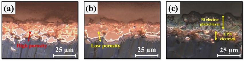
www.nature.com/scientificreports/
Figure 3. (a) The geometry of Ni electroplating model, and (b, c, d) the cathode electrode shape of 3 cases
(dimensions are represented in Table 3).
#1 #2 #3
Triangle width (μm) 1.0 2.0 3.0
Triangle height (μm) 0.5 1.0 1.5
Fillet (μm) 0.25 0.5 0.75
RMS Roughness (μm) 0.097 0.194 0.394
Table 3. Geometry dimensions and RMS roughness of cathode electrode.
roughnesses) was positioned at the lower boundary. To approximate surface roughness of sintered Cu particles
the cathode was represented as a jigsaw shape composed of isosceles triangles. Furthermore, fillets were applied
to the vertices of the aligned triangles (Fig. 3b–d). The dimensions of each case and RMS roughness are shown
in Table 3.
Through this approximation, multi-physics FEM electroplating simulation was performed at various cathode
geometries. As Ni was electroplated, the effectiveness of surface smoothening by electroplating was determined
according to 3 cases of simulated CPN electrodes.
There are several governing equations involved in the simulation p rocess29,30. First, the vertical walls on the
main electrode are considered isolated:
Ni × n = 0 (1)
Second, the flow for each of the ions in the electrolyte is determined by the Nernst-Planck equation:
N i = −Di ∇ci − zi ui Fci ∇φl (2)
ionic species, ui is the mobility of the charged species (m2/(s·J·mole)), F is Faraday’s constant (As/mole), and ϕl is
where Ni is transport vector (mol/ ( m ·s)), ci is concentration in the electrolyte (mol/m ), zi is the charge for the
2 3
the potential in the electrolyte (V). This equation allows us to calculate the distribution of Ni ion concentrations,
iso-potential lines, current density lines, and displacements of the cathode and anode surfaces.
In order to model the electrokinetics of the present Ni-electroplating simulation, the Butler-Volmer equa-
tion was used31. This equation represents the relationship of the current density of the electrode to the electrode
potential with respect to the cathodic and anodic reaction and is given by:
αc Fη αa Fη
i = io exp − − exp − (3)
RT RT
where io is exchange current density, αc and αa are cathodic & anodic transfer coefficient, F is the Faraday’s
constant, η is activation overpotential, and R is gas constant, respectively. The electrolyte initial condition and
parameters of Ni electroplating model are in Table 4.
Thus, the thickness and shape of the electroplated Ni layer can be determined through simulations with
respect to time. Therefore, the deposition and smoothening process of Ni layer can be predicted over time at
various conditions of Ni-electroplating (ex. current densities and temperatures). By utilizing simulated results,
optimal Ni-electroplating parameters were predicted prior to experimentation.
Scientific Reports | (2021) 11:14551 | https://doi.org/10.1038/s41598-021-94024-8 5
Vol.:(0123456789)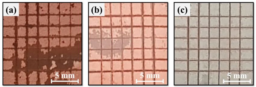
www.nature.com/scientificreports/
Parameter Value Description
Eeq_Ni − 0.26 (V) Equilibrium potential, nickel reaction
Kappa 10 (S/m) Electrolyte conductivity
M_Ni 58.69 (g/mole) Molar mass, nickel
M_Cu 63.55 (g/mole) Molar mass, copper
Rho_Ni 8908 (kg/m3) Density, nickel
Rho_Cu 8960 (kg/m3) Density, copper
io_Ni 0.1 (A/m2) Exchange current density, nickel reaction
io_H 2E-5 (A/m2) Exchange current density, hydrogen reaction
Table 4. The electrolyte initial condition and parameters of Ni electroplating model.
Figure 4. A plot of resistivity changes in Cu and CPN electrodes with respect to applied IPL irradiation energy.
Results and discussions
The evolution of surface roughness during Ni electroplating was optimized experimentally and compared to
simulation results. By optimizing the electroplating parameters for the smoothest surface, solder adhesion is
also expected to be optimized. In addition, various flash energies and their effect on the sintered structure was
characterized. The effect of ink compositions and electroplated samples was investigated to provide insight of
an individual components influence on final performance. Finally, a high-performance flexible printed track
was produced with high solderability.
IPL sintering of the Cu NPs/precursor electrodes. From previous research, it was found that Cu pre-
cursor in an amount of 30 wt.% relative to Cu NPs has the highest electrical conductivity and packing density
when sintered with IPL25. In accordance to the previous findings, 30 wt.% of Cu precursor is utilized in this study
to improve packing density and electron pathway. The specimens were sintered with various IPL irradiation
energies as shown in Fig. 4 and Table 5. The resistivity of the Cu NPs electrode and CPN electrode was the lowest
when treated with an irradiation energy of 4.70 J/cm2 and 5.13 J/cm2, respectively. It was found that the CPN
electrode had lower resistivity when the IPL energy density was over 4.46 J/cm2. However, when energy densities
above 4.94 J/cm2 and 5.41 J/cm2 were applied to Cu NP and CPN respectively, resistivity began to increase. This
was the result of oxidation on the copper electrode that formed from an excessive increase in temperature. Over-
all, the optimal IPL energy densities of 4.70 J/cm2 and 5.17 J/cm2 was selected for Cu NPs and CPN electrodes,
respectively based on the lowest resistivity readings.
The lowest resistivity of 19.98 μΩ∙cm was observed at the optimum IPL energy density (4.70 J/cm2) for the Cu
NP electrode. On the other hand, the optimum IPL energy of CPN electrodes was found to be higher than that of
Cu NP electrodes. This was due to a higher energy requirement for thermal decomposition of the Cu precursor.
The CPN electrode showed the lowest resistivity of 12.2 μΩ∙cm at its optimal IPL energy density (5.17 J/cm2).
This indicated that the voids between Cu particles were filled with Cu seed precipitated from thermal decom-
position of Cu precursor. The thermal decomposition of Cu precursor and reduction of oxides is presented in
the following equations:
Scientific Reports | (2021) 11:14551 | https://doi.org/10.1038/s41598-021-94024-8 6
Vol:.(1234567890)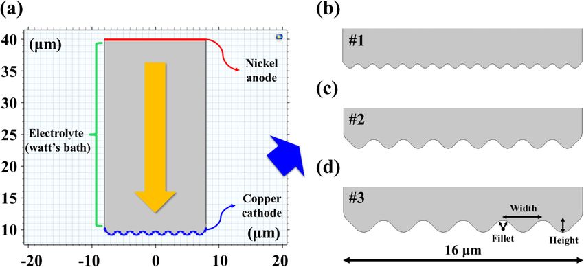
www.nature.com/scientificreports/
IPL voltage (V) IPL energy density (J/cm2) Resistivity of Cu NPs electrode (μΩ∙cm) Resistivity of CPN electrode (μΩ∙cm)
1900 3.04 2406.21 (± 277.78) –
2000 3.28 431.10 (± 58.33) –
2100 3.51 125.54 (± 25.12) 2783.88 (± 297.78)
2200 3.75 69.99 (± 13.89) 339.43 (± 52.78)
2300 3.99 42.21 (± 8.33) 153.32 (± 19.44)
2400 4.22 28.32 (± 2.78) 44.99 (± 8.33)
2500 4.46 22.77 (± 1.94) 19.71 (± 1.71)
2600 4.70 19.98 (± 0.56) 13.60 (± 1.11)
2700 4.94 31.10 (± 2.78) 12.93 (± 0.83)
2800 5.17 67.21 (± 8.33) 12.20 (± 0.28)
2900 5.41 347.77 (± 53.83) 16.93 (± 5.56)
3000 5.65 2606.32 (± 127.78) 44.99 (± 13.89)
3100 5.88 – 229.43 (± 11.11)
Table 5. IPL energy density with respect to IPL voltage at 3 ms pulse on-time and resistivity of Cu NPs
electrode and CPN electrode for each IPL energy density.
4Cu(NO3 )2 → 4CuO + 4NO ↑ + 2N2 O ↑ + 7O2 ↑ (4)
5CuO + CH3 COOH → 3Cu + Cu2 O + 2H2 O + 2CO2 ↑ (5)
4Cu2 O + CH3 COOH → 8Cu + 2H2 O + 2CO2 ↑ (6)
Cu2+ ion in Cu (II) nitrate trihydrate was reduced to Cu (I) oxide and Cu (II) oxide step by step (Eq. 4–6)32,33.
It is well documented that the reduction of Cu oxide proceeds by photo-thermal degradation of PVP b inders15.
In summary, Cu precursor is thermally decomposed by the heat generated by surface plasmonic resonance of Cu
NPs by IPL irradiation and then formed into Cu seeds by photo-thermal degradation of PVP binder.
Through this process, CPN electrodes achieved higher electrical conductivity and packing density than Cu
NP electrodes. Sintering CPN electrodes under optimal conditions significantly reduced internal voids, surface
roughness, and achieved homogeneous surface characteristics. However, the CPN electrodes still had unsatisfac-
tory mechanical and solder wetting properties. Therefore, Ni electroplating was performed to further lower the
surface roughness of the electrode and improve its mechanical properties and solderability.
Nickel electroplating. For improved soldering on printed Cu electrodes, surface roughness and internal
voids should be minimized to create a homogeneous surface. The use of Cu precursors helped fill the internal
voids in the Cu NP electrodes and helped to decrease the surface roughness compared to when only Cu NPs were
used25. The improvement of packing density and surface roughness by addition of Cu precursor is specified in
Fig. 7 and Table 9 for comparison with Ni-electroplated CPN electrode.
To further improve surface properties, Ni-electroplating was utilized. Prior to the experiment, FEM simu-
lation was performed to predict the degree of smoothening of the CPN electrode at various Ni electroplating
conditions.
FEM simulation was conducted with an important characteristic/assumptions: the shape of the Cu electrode
was approximated as shown in Fig. 3. The electroplating time required for the simulated Ni deposit surface to
reach an RMS value below 0.01 μm is taken as the time required for successful smoothening of the electrode
surface, or flattened time.
The thickness and smoothness of the Ni layer for each condition was simulated and presented graphically as
shown in Fig. 5a,b. In Fig. 5a, the electrolyte potential is visualized with a contour image at a given electroplating
condition (#1; temperature, 40 °C; current density, 2 A/dm2). As the time progresses, the potential of the electro-
lyte gradually decreased and the Ni+ ions in the electrolyte were deposited on the cathode electrode. As shown
in Fig. 5b, the roughness of the cathode gradually decreases as Ni is electroplated. For each of the 3 roughness
types (#1, #2, #3) (Fig. 3b–d, Table 3), the simulation proceeded under the conditions of 3 current densities (2,
5, 10 A/dm2) and 3 temperatures (40, 50, 60 °C).
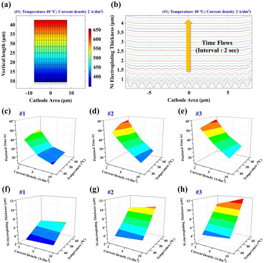
The flattened time for each condition is presented as 3D surface graphs (Fig. 5c–e, Table 6). As the surface
roughness increased (#1 → #3), it was found that the time for the cathode to be flattened increased in all condi-
tions. In addition, it was observed that the flattened time rapidly decreased as the current density increased (2 →
5 → 10 A/dm2). This is due to the faster transport of Ni ions in the electrolyte to the cathode surface at increas-
ing current densities. Furthermore, it was found that temperature did not significantly affect the flattened time.
The thickness of the Ni electroplated layer is shown in a 3D graph after a constant period of 30 s (Fig. 5f–h,
Table 7). It was found that as the surface roughness increased, the thickness of the plated Ni layer increased sig-
nificantly. If the area to be plated with Ni decreases relatively quickly (smoothens), such as case #1, the plating
reaction slows. In comparison, a rough surface such as case #3 does not achieve flattening in 30 s; due to this,
case #3 retains its roughness and higher surface area for longer and sustains an accelerated Ni deposition process.
Scientific Reports | (2021) 11:14551 | https://doi.org/10.1038/s41598-021-94024-8 7
Vol.:(0123456789)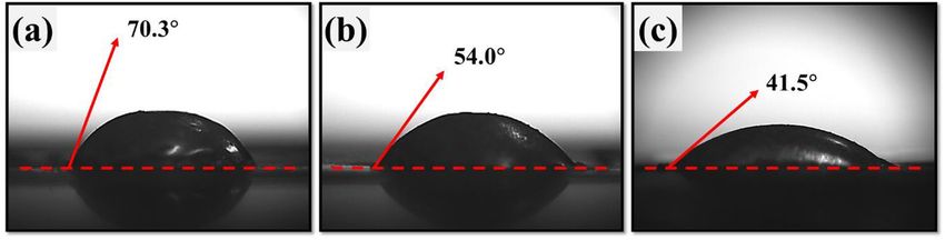
www.nature.com/scientificreports/

                                            Figure 5.  Multi-physics FEM simulation results. (a) the electrolyte potential contour image of #1 geometry, (b)
                                            the thickness of electroplated Ni layer with respect to time flows with an interval of 2 s. Time result when the
                                            cathode of (c) #1, (d) #2, (e) #3 geometry becomes flat under each current density and temperature condition.
                                            The thickness results of the electroplated cathode of (f) #1, (g) #2, (h) #3 geometry after a fixed time of 30 s.

                                                                            Temperature (°C)
                                                                            #1             #2             #3
                                             Time (s)                       40   50   60   40   50   60   40   50   60
                                                                       2    38   42   44   46   54   56   51   54   57
                                             Current Density (A/dm2)   5    22   22   24   30   32   34   35   36   38
                                                                       10   16   18   19   18   19   21   23   25   27

                                            Table 6.  Simulated flattened time of cathodes #1, #2, and #3 at various current densities and temperatures.

                                            In addition, temperature increase also increased the deposit thickness; the effect of temperature on thickness is
                                            contrasted with its limited effect in flattened time. Overall, an increase in the Ni deposit thickness indicated a
                                            growth in plated Ni particle size. As the size of the Ni particles increases, the voids between Cu particles can be
                                            quickly filled. However, if plating is allowed to continue after flattened time, excessive Ni growth will begin to
                                            increase overall roughness.
                                                Based on the simulations, it was demonstrated that the current density is related to the Ni electroplating
                                            speed, and the temperature is related to the size of the Ni particles. Therefore, after identifying these phenomena,

          Scientific Reports |   (2021) 11:14551 |                 https://doi.org/10.1038/s41598-021-94024-8                                                 8

Vol:.(1234567890)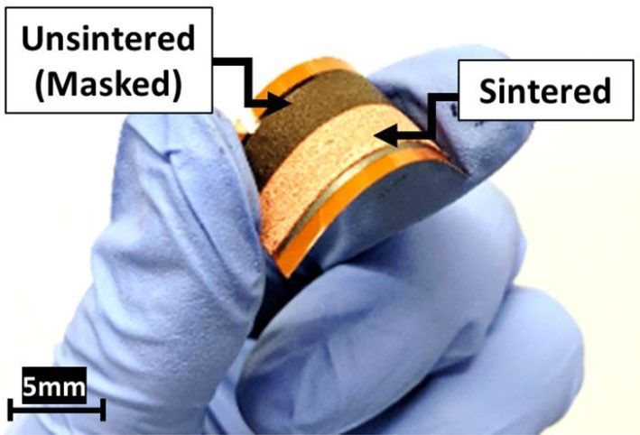
www.nature.com/scientificreports/
Temperature (°C)
#1 #2 #3
Thickness (μm) 40 50 60 40 50 60 40 50 60
2 2.40 2.55 2.73 3.25 3.50 3.83 3.6 3.9 4.3
Current Density (A/dm2) 5 3.95 4.20 4.45 5.90 6.50 6.83 6.8 7.2 7.8
10 5.50 5.80 6.15 9.10 9.50 10.1 10.1 11.0 12.0
Table 7. Simulated final thickness of the electroplated cathodes #1, #2, and #3 after a fixed time of 30 s.
Factors
Surface
Bath temperature Current density Resistivity Roughness (Sq) Thickness of Ni
Expt. no (°C) (A/dm2) Time (min) (μΩ∙cm) (μm) (μm) Adhesion
S-1 40 2 1 38.20 3.90 2.22 3B
S-2 40 2 3 32.36 3.44 3.51 4B
S-3 40 2 5 21.96 3.29 3.82 5B
S-4 40 5 1 29.68 3.28 3.51 4B
S-5 40 5 3 19.01 2.67 5.01 2B
S-6 40 5 5 12.68 2.47 7.35 1B
S-7 40 10 1 32.34 1.67 5.74 0B
S-8 40 10 3 10.54 2.28 6.36 0B
S-9 40 10 5 8.964 2.74 6.55 0B
S-10 60 2 1 45.52 4.56 2.98 5B
S-11 60 2 3 38.01 4.07 4.79 5B
S-12 60 2 5 24.31 3.43 5.63 5B
S-13 60 5 1 30.63 3.57 5.67 5B
S-14 60 5 3 18.27 2.58 7.84 3B
S-15 60 5 5 10.44 2.19 11.46 1B
S-16 60 10 1 14.78 1.45 5.41 5B
S-17 60 10 3 14.23 2.29 10.45 1B
S-18 60 10 5 10.97 2.38 13.23 0B
Table 8. Experimental results of Ni electroplating parameters on: resistivity, surface roughness, thickness, and
adhesion.
experiments were performed to confirm simulation findings. As predicted based on the simulation results, if
electroplating is performed under high current density and high temperature conditions, larger size particles
are plated faster, and thus a flatter Ni layer can be formed in a shorter period.
Following FE simulation results, Ni electroplating experiments were conducted at several parameters. As
shown in Table 8, various specimens were prepared with 3 independent electroplating variables: temperature,
current density, and plating time. In addition, dependent variables: resistivity, surface roughness, thickness, and
adhesion of the Ni layer were measured for the 18 specimen types.
The resistivity of bulk Ni is about 7 μΩ∙cm, but when electroplated, about 3 times the resistivity has been
previously observed34–37. When electroplating Ni onto a CPN electrode with an initial resistivity of 12.2 μΩ∙cm,
the electrodes final resistivity differed depending on the plating conditions. It was found that as the thickness
of the Ni layer increased, the resistivity decreased and approached the initial resistivity of the CPN electrode.
In the cases of S-6, S-8, S-9, S-15, S-17 and S-18 with very thick Ni layer, the resistivity was lower than that of
the initial CPN electrode. This is due to the Ni filling in the CPN electrode increasing electron pathways. How-
ever, the electroplating proceeded excessively inside of the Cu electrode, weakening and almost eliminating the
adhesion between the electrode and the substrate. S-16 is the only case in which substrate adhesion was retained
while maintaining a relatively low resistivity of 14.78 μΩ∙cm and a low surface roughness.
At a fixed plating time, the surface roughness, thickness, and adhesion of plated Ni all increased with increased
temperatures. This is in-line with simulation results. Under the same conditions, when the temperature increased,
the thickness of the Ni electroplated layer also increased (Fig. 5f–h). Additionally, increasing current density
increased the thickness of the Ni deposit and formed a smoother surface. Furthermore, an increase in plating
time led to an increase in thickness and a decrease in roughness.
Another phenomenon was observed by varying current density while fixing other independent variables.
Increasing current density resulted in an increase of the plating’s final thickness, but it also resulted in an increase
to the plating’s final roughness. At a higher current density of 10 A/dm2, the cracks on the surface of the CPN
electrode had been quickly filled by large Ni particles. Continued growth of the Ni deposits led to a high surface
roughness. Over longer periods of plating time, the surface roughness would continue to increase beyond the
Scientific Reports | (2021) 11:14551 | https://doi.org/10.1038/s41598-021-94024-8 9
Vol.:(0123456789)
www.nature.com/scientificreports/

                                            Figure 6.  Surface morphology observations of (a) IPL sintered Cu NP electrode, (b) IPL sintered CPN
                                            electrode, and (c) Ni electroplated CPN electrode (S-16). Optical 3D profile images of an (d) IPL sintered Cu NP
                                            electrode, (e) IPL sintered CPN electrode, and (f) Ni electroplated CPN electrode (S-16).

                                                                  IPL sintered                IPL sintered              Ni-electroplated
                                             Label                Cu NP electrode             CPN electrode             CPN electrode (S-16)
                                             Sq (μm)              12.04 ± 2.01                3.90 ± 0.44               1.45 ± 0.31

                                            Table 9.  Surface characterization parameters of three kinds of electrodes (Observation Area:
                                            831 μm × 623 μm).

                                            initial roughness of the CPN electrode. At a lower current density of 5A/dm2, it was observed that smaller Ni
                                            particles had gradually filled the cracks of the CPN electrodes surface and created a smooth Ni surface. The
                                            same trend occurred under all conditions, independent of temperature. In the case of S-16, electroplating was
                                            performed at a high temperature of 60 °C and a high current density of 10 A/dm2, resulting in relatively large
                                            diameter Ni particles being deposited on the electrodes surface at a high rate. Due to case S-16’s low plating
                                            time of 1 min, it was possible to fill the cracks in the CPN electrodes surface with large Ni particles while still
                                            maintaining a relatively low surface roughness. In the cases of S-17 and S-18, which had proceeded for more
                                            than 3 min, the Ni growth formed was excessively thick and as a result, the electrodes final roughness had drasti-
                                            cally increased. In addition to the increased roughness, Ni had been deposited inside the electrode, leading to
                                            an inhibition of adhesion to occur between the CPN and the substrate. In summary, the S-16 specimen showed
                                            the best balance of surface roughness, plating thickness, and adhesion to the substrate.
                                                 Based on the superior performance of the S-16 Ni-electroplated CPN electrodes, further samples were fab-
                                            ricated with S-16 parameters. The S-16 Ni-electroplated CPN electrodes are compared with non-plated Cu NP
                                            electrodes and CPN electrodes. In addition, S-16 electroplating conditions were utilized for selective plating
                                            experiments. By using aluminum foil, half of the printed CPN electrode was masked then exposed to IPL sin-
                                            tering at the optimal 2800 V 3 ms on-time flash. During electroplating, alligator clips were placed at the middle
                                            junction of the two halves and immersed in the same electrolyte.
                                                 Achieving selective plating of only the sintered potion presents significant savings in circuit manufacturing
                                            time. Like negative photoresists, only the printed CPN surfaces exposed to IPL irradiation will accommodate
                                            Ni plating. This can be utilized to create re-usable patterned masks with the desired circuit pattern to be plated.
                                            Under S-16 conditions, Ni plating was not observed in the non-sintered portion of the electrode while the
                                            sintered half plated normally. As expected, the non-conductive portion is unable to accommodate the negative
                                            charge provided by the power supply potential. This lack of conductivity meant the non-sintered portion could
                                            not participate in the reduction of Ni cations onto its surface. After over 5 min of plating time at S-16 conditions,
                                            the non-sintered portion exhibited no Ni-deposition. Furthermore, the non-sintered portion lost adhesion to the
                                            substrate and coherency while in the electrolyte. Simple shaking was able to remove the non-sintered portion,
                                            leaving behind a robust selectively Ni-plated CPN electrode.
                                                 Using a 3D optical profiler, the surface roughness of three kinds of electrodes were compared (Fig. 6). Pure
                                            Cu NP electrodes had a significantly higher surface roughness of Sq = 12.04 μm, as shown in Fig. 6a, and Table 9.
                                            Alternatively, the surface roughness of the CPN electrode was reduced to Sq = 3.90 μm as a result of Cu seeds that
                                            filled the voids between Cu particles. In addition, when Ni electroplating was performed on the CPN electrode,
                                            its surface roughness was drastically reduced to Sq = 1.45 μm.

          Scientific Reports |   (2021) 11:14551 |               https://doi.org/10.1038/s41598-021-94024-8                                                   10

Vol:.(1234567890)
www.nature.com/scientificreports/
Figure 7. SEM analysis of an (a) IPL sintered Cu NPs electrode, (b) IPL sintered CPN electrode, and (c) Ni
electroplated CPN electrode (S-16). (d) EDS mapping for a Ni electroplated CPN electrode and an (e) EDS
spectrum for Ni electroplated CPN electrode (S-16).
The changes in roughness were observed in further detail through SEM analysis. Figure 7a shows the surface
of IPL sintered Cu NPs. Although necking occurred between the particles, there were many voids and cracks still
present between these particles. On the other hand, as seen in Fig. 7b, when Cu seeds are used as the precursor,
the connections between Cu NPs are much larger, resulting in a more densely sintered material. Finally, in the
case of Fig. 7c, it was observed that the Ni plated surface was smooth relative to the other electrodes.
EDS analysis was performed to confirm that Ni was uniformly deposited onto the surface of the CPN elec-
trode. Figure 7d shows the EDS mapping for the distribution of Cu and Ni while Fig. 7e shows the corresponding
EDS spectrum. On the EDS map, the blue Ni component is shown to cover the entire surface, with the yellow
Cu component being detected in between the Ni layer. However, when this was examined by the EDS spectrum,
the detected Cu peak was relatively negligible compared to the detected Ni peak. From this, the conclusion was
drawn that the Ni layer covers the majority of the CPN electrode.
To demonstrate the densification of each electrode, SEM images were processed by adjusting the brightness
of the images. Through the emphasized contrast between black and white, solids were represented by white
regions and the voids were represented by black regions. The densification of the electrode was estimated by
finding the ratio of the number of white pixels in the images to the total number of pixels in the image. 79.4%
of the 336,788 total pixels were white in the processed Cu NP electrode image, while 98.6% of the 336,788 total
pixels were white in the CPN electrode image. It was therefore concluded that the voids within the Cu NP elec-
trodes were decreased from 20.6 to 1.4% when the Cu precursor was added. In the case of the Ni-plated CPN
electrode, 100% of the 336,788 pixels in the image were white, indicating that the voids within the electrode had
been filled in. It was demonstrated that voids present between Cu NPs could be largely eliminated by subjecting
Ni electroplating to CPN electrodes.
These results were further confirmed through cross-sectional observation of three kinds of electrodes (Fig. 8).
Each specimen was immersed in liquid nitrogen for 10 min and then split to expose their cross-sections and
observe them through an optical microscope. The cross section of the Cu NP electrode revealed that the particles
within were sintered, but many voids between the particles were still observed (Fig. 8a). In the case of the CPN
electrode, its porosity was reduced due to the Cu seeds that filled the voids between Cu NPs, while also retaining
a smooth surface (Fig. 8b). As shown in Fig. 8c, it was observed that the Ni plated CPN electrode was covered
in a homogenous Ni layer. In addition, it was observed that the Ni layer penetrated the inside of the Ni plated
CPN electrode and filled the fine cracks of the CPN electrode. Therefore, it can be inferred that the entire surface
of Cu is covered with Ni, and a strong bonding force acts between the interfaces. Since a homogeneous layer of
Ni metal has formed on the surface, the Ni plated CNP electrode was theorized to have better solder adhesion.
In order to perform as a solderable electrode, there must be a strong bonding force between the solder-Ni layer
and the Ni layer-CPN electrode. Therefore, ASTM D3359 adhesion testing was performed on three electrodes: Cu
NPs (Fig. 9a), CPN (Fig. 9b) and Ni-electroplated CPN (Fig. 9c). In the case of the Cu NP electrode, the solder-
electrode bonding strength was too weak to form a viable connection due to its rough surface and high porosity.
During the adhesion test, more than 35% of the grids surface area flaked off, indicating 2B adhesion. In the case
of the CPN electrode, it was found that over 15% of the grids surface area gradually flaked off, indicating 3B
Scientific Reports | (2021) 11:14551 | https://doi.org/10.1038/s41598-021-94024-8 11
Vol.:(0123456789)www.nature.com/scientificreports/
Figure 8. Cross-sectional observation of an (a) IPL sintered Cu NPs electrode, (b) IPL sintered CPN electrode,
and (c) Ni electroplated CPN electrode (S-16).
Figure 9. ASTM D 3359 Adhesion test for an (a) IPL sintered Cu NP electrode, (b) IPL sintered CPN electrode,
and (c) Ni electroplated CPN electrode (S-16).
Figure 10. Solder contact angle measurement of an (a) IPL sintered Cu NPs electrode, (b) IPL sintered CPN
electrode, and (c) Ni electroplated CPN electrode (S-16).
adhesion. In the case of the Ni electroplated CPN electrode, the electrode completely maintained its Ni surface,
indicating 5B adhesion. This confirmed that both the mechanical and surface morphology characteristics of Cu
NP electrodes can be improved through Ni electroplating treatment.
Wetting and Mechanical properties of the Ni‑electroplated CPN electrode. To investigate the
solderability of Ni-electroplated CPN electrodes, wetting and solder shear tests were conducted. The wetting
test was conducted by melting 1 cm of solder wire with a soldering iron, dropping the solder onto the electrode,
and then measuring the contact angle between the solder and the electrode. As shown in Fig. 10a, the solder
dropped onto the Cu NP electrode retained a relatively low-width elliptic shape resulting in a contact angle of
70.3° between the solder and the electrode. In comparison, the CPN electrode retained a contact angle of 54.0°
between the solder and the electrode as shown on Fig. 10b. The Ni-electroplated CPN electrode exhibited the
most solder-wet behaviour with an even further decreased contact angle of 41.5° between the solder and the
electrode as shown in Fig. 10c. The decreased surface roughness and homogenous Ni surface was attributed for
the improved solder wetting properties of the electroplated CPN electrode.
Shear tensile testing was performed to quantitatively determine the bonding strength between solder and the
electrode. Solder shear strength was measured using a tensile tester as shown in Fig. 11. Through this experiment,
Scientific Reports | (2021) 11:14551 | https://doi.org/10.1038/s41598-021-94024-8 12
Vol:.(1234567890)www.nature.com/scientificreports/
Figure 11. Shear strength tensile test between solder and electrodes. Ni-electroplating was performed under
S-16 conditions.
the relationship between the electrode’s treatment and the electrodes solder wettability was determined. The
highest maximum shear strength of solder was observed on the Ni-electroplated CPN electrodes at 2.75 MPa.
Based on these experimental results, it was confirmed that the mixing of Cu precursor and Ni electroplating
significantly lowered the roughness of the electrode surface, and thus significantly increased its bonding strength
with the solder. This is attributed to an increase in the electrodes solder wetting properties, resulting in a higher
contact area and thus, a stronger solder connection.
Through the present investigations, sintering and electroplating parameters were optimized at 2800 V and
S-16 conditions, respectively. IPL sintering at 2800 V provided the necessary energy required to sufficiently sinter
the printed electrodes while avoiding excessive oxidation at higher energies. The addition of Cu precursor was
found to improve conductivity by seeding Cu and increasing the overall packing density and electron pathway.
Electroplating at higher temperatures (60 °C) and current density (10 A/dm2) facilitated rapid void filling. Lim-
iting the plating time to 1 min avoided excessive Ni growth which would increase surface roughness at longer
electroplating times. Selective electroplating was demonstrated by utilizing a simple mask during IPL sintering
to create conductive and electroplating surfaces while rejecting non-sintered portions (Fig. 2).
By utilizing Cu precursors and electroplating: solderability, adhesion, and mechanical strength was improved
to produce a robust and conductive electrode. An important detail to note is that the Ni electroplated CPN elec-
trode shearing test did not fail between the solder and the Ni surface, nor between the Ni surface and the CPN
electrode. In fact, the shear test failed between the CPN electrode and the PI substrate. From this observation, it
was concluded that the solderability was maximized for this type of electrode without further improvements to
adhesion between the electrode and the substrate. Although chosen for its mechanical and electrical properties,
there are other alternative plating metals instead of Ni. Future works can be performed to explore alternative plat-
ing metals to reduce cost while retaining the mechanical and conductive properties of Ni plated CPN electrodes.
Conclusions
We investigated the feasibility of nickel plating on IPL sintered hybrid copper electrodes. The analytical and
experimental tests were conducted to observe the morphology characteristics of different electrodes to improve
the solderability of printed Cu electrodes. Cu NPs were mixed with 30 wt.% of Cu (II) Nitrate Trihydrate precur-
sor to fabricate the Cu Precursor/NPs (CPN) electrodes. It was found that the resistivity of the CPN electrodes
was decreased due to the reduction and precipitation of Cu precursor between Cu NPs. Ni electroplating pro-
cess was applied to complement the weak mechanical properties of IPL sintered Cu, which further improved
the surface morphology characteristics and improved solderability. Through multi-physics FEM electroplating
simulations, effects of different parameters on electroplating were identified. Based on the mechanistic insight
provided by simulation results, Ni-electroplating was performed for improved solderability and mechanical
properties. The surface roughness was drastically reduced to Sq = 1.45 μm in optimized conditions (temperature,
60 °C; cathode current density, 10 A/dm2; plating time, 1 min). Experimental solder shear tensile test showed
a shear strength of Ni-electroplated Cu NPs/Precursor electrodes as 2.75 MPa. Reducing the roughness on a
surface through Ni-electroplating leads to improved solder wetting. Moreover by applying a mask during IPL
sintering, the electrode showed selective nickel plating only on the sintered portion (i.e., the conductive region);
this paves the new way for patterned mask flashing followed by selective electroplating to streamline the circuit
manufacturing process. It is expected that the proposed approach can also be used in reflow soldering of electrical
components for IPL based printed electrodes and circuits.
Received: 2 March 2021; Accepted: 23 June 2021
Scientific Reports | (2021) 11:14551 | https://doi.org/10.1038/s41598-021-94024-8 13
Vol.:(0123456789)www.nature.com/scientificreports/
References
1. Subramanian, V. et al. Progress toward development of all-printed RFID tags: Materials, processes, and devices. Proc. IEEE 93,
1330–1338 (2005).
2. David, M., Ranasinghe, D. C. & Larsen, T. In 2011 IEEE International Conference on RFID. 176–183 (IEEE).
3. Comiskey, B., Albert, J. D., Yoshizawa, H. & Jacobson, J. An electrophoretic ink for all-printed reflective electronic displays. Nature
394, 253–255 (1998).
4. Zyung, T. et al. Flexible organic LED and organic thin-film transistor. Proc. IEEE 93, 1265–1272 (2005).
5. Kondo, Y., Tanabe, H. & Otake, T. Novel electrochromic polymer for electronic paper. IEICE Trans. Electron. 93, 1602–1606 (2010).
6. Yang, Y. & Heeger, A. Polyaniline as a transparent electrode for polymer light-emitting diodes: Lower operating voltage and higher
efficiency. Appl. Phys. Lett. 64, 1245–1247 (1994).
7. Haight, R. A. & Troutman, R. R. (Google Patents, 1998).
8. Leem, D. S. et al. Efficient organic solar cells with solution-processed silver nanowire electrodes. Adv. Mater. 23, 4371–4375 (2011).
9. Zou, J., Yip, H.-L., Hau, S. K. & Jen, A.K.-Y. Metal grid/conducting polymer hybrid transparent electrode for inverted polymer
solar cells. Appl. Phys. Lett. 96, 96 (2010).
10. Liao, Y. et al. Highly conductive carbon-based aqueous inks toward electroluminescent devices, printed capacitive sensors and
flexible wearable electronics. RSC Adv. 9, 15184–15189 (2019).
11. Karim, N., Afroj, S., Tan, S., Novoselov, K. S. & Yeates, S. G. All inkjet-printed graphene-silver composite ink on textiles for highly
conductive wearable electronics applications. Sci. Rep. 9, 1–10 (2019).
12. El-Sayed, M. A. Some interesting properties of metals confined in time and nanometer space of different shapes. Acc. Chem. Res.
34, 257–264 (2001).
13. Link, S. & El-Sayed, M. A. Shape and size dependence of radiative, non-radiative and photothermal properties of gold nanocrystals.
Int. Rev. Phys. Chem. 19, 409–453 (2000).
14. Hartland, G. V. Coherent excitation of vibrational modes in metallic nanoparticles. Annu. Rev. Phys. Chem. 57, 403–430 (2006).
15. Ryu, J., Kim, H.-S. & Hahn, H. T. Reactive sintering of copper nanoparticles using intense pulsed light for printed electronics. J.
Electron. Mater. 40, 42–50 (2011).
16. Hwang, H.-J., Chung, W.-H. & Kim, H.-S. In situ monitoring of flash-light sintering of copper nanoparticle ink for printed elec-
tronics. Nanotechnology 23, 485205 (2012).
17. Hwang, Y.-T., Chung, W.-H., Jang, Y.-R. & Kim, H.-S. Intensive plasmonic flash light sintering of copper nanoinks using a band-
pass light filter for highly electrically conductive electrodes in printed electronics. ACS Appl. Mater. Interfaces 8, 8591–8599 (2016).
18. Jang, Y.-R. et al. Selective wavelength plasmonic flash light welding of silver nanowires for transparent electrodes with high con-
ductivity. ACS Appl. Mater. Interfaces. 10, 24099–24107 (2018).
19. Salam, B. & Lok, B. In 2008 15th International Symposium on the Physical and Failure Analysis of Integrated Circuits. 1–4 (IEEE).
20. Chan, H.-J., Huang, B.-C., Wang, L.-W., Liao, K.-H. & Lo, C.-Y. Porosity reduction in inkjet-printed copper film by progressive
sintering on nanoparticles. Thin Solid Films 627, 33–38 (2017).
21. Tuck, J., Korsunsky, A. M., Davidson, R., Bull, S. J. & Elliott, D. Modelling of the hardness of electroplated nickel coatings on copper
substrates. Surf. Coat. Technol. 127, 1–8 (2000).
22. Mosayebi, S., Rezaei, M. & Mahidashti, Z. Comparing corrosion behavior of Ni and Ni-Mo electroplated coatings in chloride
mediums. Colloids Surfaces A Physicochem. Eng. Aspects 124654 (2020).
23. Liu, C.-S., Su, F.-H. & Liang, J.-Z. Fabrication of Co–Ni–P film with excellent wear and corrosion resistance by electroplating with
supercritical CO2 emulsion. Trans. Nonferrous Metals Soc. China 28, 2489–2498 (2018).
24. Zhou, H.-H. et al. Pulse electroplating of Ni-WP coating and its anti-corrosion performance. Trans. Nonferrous Metals Soc. China
28, 88–95 (2018).
25. Chung, W.-H., Hwang, H.-J. & Kim, H.-S. Flash light sintered copper precursor/nanoparticle pattern with high electrical conduc-
tivity and low porosity for printed electronics. Thin Solid Films 580, 61–70 (2015).
26. Young, C. & Struyk, C. Deposition of Nickel–Cobalt alloys from chloride solutions. Trans. Electrochem. Soc. 89, 383 (1946).
27. Wojciechowski, J., Baraniak, M., Pernak, J. & Lota, G. Nickel coatings electrodeposited from watts type baths containing quaternary
ammonium sulphate salts. Int. J. Electrochem. Sci. 12, 3350–3360 (2017).
28. Mattsson, E. & Bockris, J. M. Galvanostatic studies of the kinetics of deposition and dissolution in the copper + copper sulphate
system. Trans. Faraday Soc. 55, 1586–1601 (1959).
29. Lima, F., Mescheder, U. & Reinecke, H. Simulation of current density for electroplating on silicon using a Hull cell. Solar Cells 6,
7 (2012).
30. Yan, D. Computational Simulation of Copper (Cu) and Nickel-Copper (Ni–Cu) Alloy Electrodeposition (2019).
31. Shourije, S. & Bahrololoom, M. Comparison of effects of simulated electric field interference and presence of a barrier in the nickel
electroplating process to experimental data. Trans. IMF 98, 303–313 (2020).
32. Lee, B. et al. Hybrid copper complex-derived conductive patterns printed on polyimide substrates. Met. Mater. Int. 18, 493–498
(2012).
33. Kim, M. H., Lim, B., Lee, E. P. & Xia, Y. Polyol synthesis of Cu2O nanoparticles: use of chloride to promote the formation of a cubic
morphology. J. Mater. Chem. 18, 4069–4073 (2008).
34. Luo, J. et al. Effects of process conditions on properties of electroplated Ni thin films for microsystem applications. J. Electrochem.
Soc. 153, D155 (2006).
35. Safranek, W. H. The properties of electrodeposited metals and alloys: A handbook. Am. Electroplaters Surface Finish. Soc. 1986,
550 (1986).
36. Aesar, A. (Ward Hill, MA, 2003).
37. Safranek, W. Structure and property relationships for bulk electrodeposits. J. Vac. Sci. Technol. 11, 765–770 (1974).
Acknowledgements
The authors acknowledge the financial support of the Natural Sciences and Engineering Research Coun-
cil of Canada (NSERC). This work was supported by the Korea Institute of Energy Technology Evaluation
and Planning(KETEP) and the Ministry of Trade, Industry & Energy(MOTIE) of the Republic of Korea (No.
20206910100160). This research was also supported by the MOTIE (Ministry of Trade, Industry, and Energy) in
Korea, under the Fostering Global Talents for Innovative Growth Program (P0008748, Global Human Resource
Development for Innovative Design in Robot and Engineering) supervised by the Korea Institute for Advance-
ment of Technology (KIAT).
Author contributions
All authors contributed to the writing and development of the manuscript. Authors Yong-Rae Jang and Robin
Jeong performed data collection and analysis for all physical experiments. Author Yong-Rae Jang performed
Scientific Reports | (2021) 11:14551 | https://doi.org/10.1038/s41598-021-94024-8 14
Vol:.(1234567890)You can also read