FIELD EMISSION FROM TWO-DIMENSIONAL GEAS - ART ...
←
→
Page content transcription
If your browser does not render page correctly, please read the page content below
Journal of Physics D: Applied Physics

PAPER

Field emission from two-dimensional GeAs
To cite this article: Antonio Di Bartolomeo et al 2021 J. Phys. D: Appl. Phys. 54 105302

View the article online for updates and enhancements.

                             This content was downloaded from IP address 141.108.253.127 on 18/02/2021 at 16:32
Journal of Physics D: Applied Physics
J. Phys. D: Appl. Phys. 54 (2021) 105302 (7pp) https://doi.org/10.1088/1361-6463/abcc91
Field emission from two-dimensional
GeAs
Antonio Di Bartolomeo1,2,7, Alessandro Grillo1,2, Filippo Giubileo2, Luca Camilli3,
Jianbo Sun4, Daniele Capista5 and Maurizio Passacantando5,6
1
Department of Physics ‘E.R. Caianiello’ and Interdepartmental Centre NanoMates, University of
Salerno, via Giovanni Paolo II, Fisciano 84084, Italy
2
CNR-SPIN Salerno, via Giovanni Paolo II, Fisciano 84084, Italy
3
Dipartimento di Fisica, Università degli studi di Roma ‘Tor Vergata’, via della Ricerca Scientifica 1,
Roma 00133, Italy
4
Department of Physics, Technical University of Denmark, Ørsteds Plads, Kgs. Lyngby 2800, Denmark
5
Department of Physical and Chemical Sciences, University of L’Aquila, via Vetoio, Coppito, L’Aquila
67100, Italy
6
CNR-SPIN L’Aquila, via Vetoio, Coppito, L’Aquila 67100, Italy
E-mail: adibartolomeo@unisa.it
Received 16 October 2020, revised 10 November 2020
Accepted for publication 20 November 2020
Published 22 December 2020
Abstract
GeAs is a layered material of the IV–V groups that is attracting growing attention for possible
applications in electronic and optoelectronic devices. In this study, exfoliated multilayer GeAs
nanoflakes are structurally characterized and used as the channel of back-gate field-effect
transistors. It is shown that their gate-modulated p-type conduction is decreased by exposure to
light or electron beam. Moreover, the observation of a field emission (FE) current demonstrates
the suitability of GeAs nanoflakes as cold cathodes for electron emission and opens up new
perspective applications of two-dimensional GeAs in vacuum electronics. FE occurs with a
2
turn-on field of ∼80 V µm−1 and attains a current density higher than 10 A cm− , following the
general Fowler–Nordheim model with high reproducibility.
Keywords: GeAs, 2D materials, field-effect transistor, field emission, electrical conductivity,
anisotropy
(Some figures may appear in colour only in the online journal)
1. Introduction have been synthesized by combining Ge and As in vacuum
at high temperature (>1370 K) [2] and have been exfoliated
Germanium arsenide (GeAs) has emerged as an interest- in liquid phase or mechanically to obtain multilayer or few-
ing layered compound of IV–V groups with a crystal struc- layer nanosheets [3]. First-principles calculations and UV-
ture belonging to the centrosymmetric monoclinic C2/m(12) visible absorption spectroscopy have demonstrated that GeAs
space group and strong in-plane anisotropy [1, 2]. In GeAs, nanosheets have a bandgap that increases significantly as the
every Ge atom is coordinated to three As atoms and another number of layers decreases, from 0.6 eV for the bulk up to
Ge atom, while every As atom is coordinated to three Ge 2.1 eV for the monolayer [3, 4]. Remarkably, while the mono-
atoms (figure 1(a)). Each GeAs monolayer is terminated by layer has a direct bandgap, the multilayers are predicted to
As atoms and interacts with neighboring layers by weak have a quasi-direct bandgap.
van der Waals forces. The small interlayer cohesion energy The electrical properties of multilayer GeAs nanosheets
(0.191 eV atom−1 ) allows easy exfoliation. Ingots of GeAs have been measured to reveal their two-dimensional (2D)
carrier transport behavior [5] and anisotropic electrical con-
duction strongly affected by impurities [6]. Using multilayer
7
Author to whom any correspondence should be addressed. GeAs field-effect transistors (FETs), it has been proved that the
1361-6463/21/105302+7$33.00 1 © 2020 IOP Publishing Ltd Printed in the UK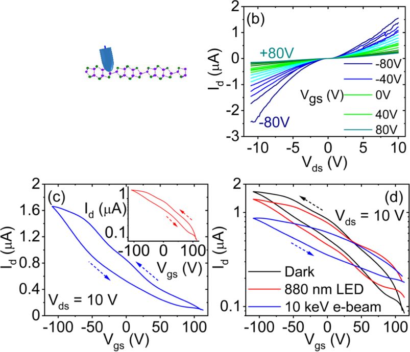
J. Phys. D: Appl. Phys. 54 (2021) 105302                                                                                    A Di Bartolomeo et al

temperature-dependent conductivity can be described by the
coexistence of variable range hopping among defect-induced
bandgap states and band-like transport [3, 5, 6]. The carrier
mobility in GeAs is higher along the zig-zag direction and
typically in the range 0.1–10 cm2 V−1 s−1 [5–7]. The aniso-
tropic crystal structure of GeAs leads also to highly anisotropic
thermal conductivity [2], mechanical response [8] and optical
properties [7]. Moreover, stable and large photocurrents with
rapid on/off switching as well as linear dichroism and polar-
ized photodetection indicate that GeAs is a promising material
for high-performance optoelectronic nanodevices, particularly
for polarization optical applications [3, 9]. GeAs nanosheets
have also shown promising photoelectrochemical water split-
ting capability under visible light irradiation [3, 10].
    In the present study, we characterize crystal structure
and symmetry of mechanically exfoliated multilayer GeAs
nanosheets. FETs are obtained by contacting GeAs nanoflakes
with Au electrodes and/or metallic tips. We investigate the
field emission (FE) properties of GeAs nanoflakes, taking
advantage from a nanotip inside a scanning electron micro-
scope (SEM) chamber that is used as the anode for local FE
characterization [11, 12].
    FE is the extraction of electrons from a semiconducting or
metallic material under the application of an electric field. As a
macroscopic manifestation of a quantum effect, FE offers sig-
nificant scientific interests in material science and is exploited
in many applications such as electron microscopy, electron               Figure 1. (a) Side view for the crystal structure of layered GeAs. (b)
spectroscopy, e-beam lithography as well as in vacuum elec-              SEM image showing a GeAs flake in tiny contact with the Au
tronics for nanoscale FE transistors, displays and microwave             electrode (top marker). The inset shows the same flake contacted by
generation or for x-ray tubes [13–19]. The externally applied            a tungsten tip (Tip 1); a second tungsten tip (Tip 2) is on the Au
                                                                         marker. The Au marker is used as the cathode while Tip 1 is used as
electric field reduces the barrier for electron escape from              the anode in the electrical measurements. (c) SEM image of another
the material to vacuum. FE is favored from electrically and              GeAs flake used for field emission measurements, with anode tip at
thermally highly conducting materials with low work func-                hundreds nm from the flake. (d) AFM profile of the GeAs flake of
tion and nanometer rough surface that give rise to local field           figure (c), showing the nanosheet thickness of 6 nm. (e) XRD
enhancement. Hence, the intrinsic doping, the sharp edge and             pattern in Bragg–Brentano geometry and (f) Raman spectrum of the
                                                                         same GeAs flake, measured in the parallel configuration.
the low electron affinity below 4 eV of GeAs nanosheets are
beneficial for FE. Moreover, the GeAs electron affinity, which
results in a low tunneling barrier, decreases with the number of
layers, being only 3.17 eV for the bilayer and 2.78 eV for the           with the Au marker. The contact with the Au marker is wider
monolayer [3]. Despite that, we note that FE from 2D GeAs                for the flake of figure 1(c), which has a uniform thickness of
has not been reported so far.                                            about 6 nm, corresponding to about ten monolayers, as shown
    In this work, we show that a high and reproducible FE cur-           in figure 1(d) by its height profile as measured by atomic force
rent can be extracted from the edge of GeAs nanoflakes.                  microscopy (AFM).
                                                                             The electrical conduction of the GeAs flakes was meas-
                                                                         ured inside the SEM chamber at pressure below 10−6 Torr
2. Materials and methods                                                 and at room temperature. The flakes were gently contacted by
                                                                         means of two piezo-driven tungsten nanotips (Tip 1 and Tip 2)
Ultrathin GeAs flakes were mechanically exfoliated from bulk             with nanometric movement control, used as the anode and the
GeAs single crystals using a standard adhesive tape method               cathode, respectively. Such tips were connected to a semicon-
[20]. The nanoflakes were exfoliated onto degenerately p-                ductor parameter analyzer Keithley 4200-SCS, used as source-
type doped silicon substrates, covered by 300 nm thick SiO2 .            meter unit. To take advantage of the usually wider and more
The SiO2 /Si substrate was endowed with patterned markers of             stable electrical contact produced by the van de Waals force
5 nm Ni/50 nm Au, which were previously defined by pho-                  between the GeAs nanosheet and the Au marker, we often
tolithography and lift-off. Sometimes, the transferred flakes            chose flakes in electrical contact with a marker. In this config-
ended up partially over the SiO2 layer and partially over an             uration, the Au marker was used as the cathode and the tung-
Au marker establishing an electrical contact with it. The SEM            sten tip in direct contact with the flake was used as the anode
images of two typical flakes are shown in figures 1(b) and (c).          (inset of figure 1(b)). The Si substrate offered a third terminal
In particular, figure 1(b) displays a flake with minimal overlap         and was used as the gate in a three-probe FET configuration.

                                                                     2
J. Phys. D: Appl. Phys. 54 (2021) 105302 A Di Bartolomeo et al
A simple variation of this setup, with the tungsten tip (anode)
detached from the flake and positioned at a fixed distance from
the GeAs nanosheet (figure 1(c)) allowed the measurement of
the local FE current from the nanoflake.
The x-ray diffraction (XRD) was performed by means of
a Bruker D5000 system equipped with Cu Kα (wavelength
λ = 0.154 nm) line excitation source. The patterns were
acquired in Bragg–Brentano mode that enables measurements
of the crystal orientation of the GeAs flakes with respect to the
substrate surface as well as of their lattice parameters. Raman
spectroscopy measurements were performed using a LabRam
high-resolution Micro Raman apparatus by Jobin Yvon with
λ0 = 632 nm excitation.
3. Results and discussion
3.1. Structural and crystal symmetries characterization
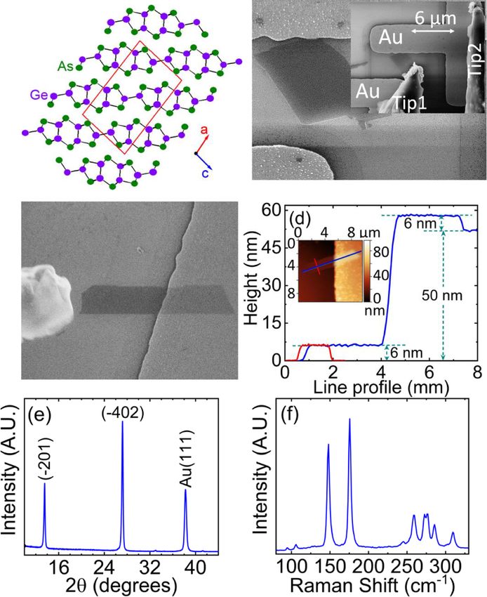
Figure 1(e) reports the XRD pattern of the sample that we used Figure 2. (a) Schematic of the back-gate transistor used for the
to determine the unit cell parameters by Rietveld refinement. electrical characterization of the GeAs nanosheets. Electrical
characterization of the nanoflake of figure 1(b): (b) output
The peaks identified in figure 1(e) correspond to the (−201)
characteristics Id − Vds for stepping Vgs , showing gate current
and (−402) base-centered monoclinic structure of GeAs, and modulation; (c) transfer characteristics Id − Vgs for a fixed Vds with
the (111) planes of Au from the Au markers. The structure the current on linear and logarithmic scale (inset); (d) transfer
of GeAs was solved in the monoclinic space group C2/m characteristics in dark, under 880 nm–265 µW cm−2 LED light, and
(12) (JCPDS 011–0524) and the obtained lattice parameters after 10 keV–10 pA electron (e-beam) irradiation. All
are: a = 1.5552 nm, b = 0.3761 nm, c = 0.9524 nm and measurements are performed at low pressure below 10−6 Torr and
◦ at room temperature.
βac
b = 101.255 . Furthermore, the XRD spectrum confirms an
interlayer spacing of 0.66 nm in agreement with previously
reported data [20]. These observations lead to the ball and stick
model of figure 1(a), showing the GeAs crystal structure in the
projection plane (010) along with the cell edges (red line). In p-type conduction of the GeAs nanoflake is confirmed by fig-
figure 1(a), two different geometric orientations of the Ge–Ge ure 2(c), reporting the transfer characteristic, Id − Vgs curve for
bond can be clearly distinguished from the crystalline struc- a fixed Vds , and showing that the transistor current decreases
ture of the GeAs: one bond parallel and the other one per- for increasing Vgs . The modulation of the current is limited
pendicular to the layer plane that is an evidence of the aniso- to one order of magnitude, despite the quite large Vgs range,
tropic nature of GeAs crystal structure. The Raman spectrum consistently with the multilayer nature of the GeAs flake cor-
shown in figure 1(f) evidences multiple Raman active modes responding to a bandgap around several hundred meV. From
peaks due to highly asymmetric structure, with eight of them the slope of the transfer characteristic, we estimated the field-
being Ag modes (95 cm−1 , 106 cm−1 , 148 cm−1 , 175 cm−1 , effect mobility as µ = WCoxL Vds dVdId
gs
≈ 0.6 cm2 V−1 s−1 , where
273 cm−1 , 276 cm−1 , 285 cm−1 and 309 cm−1 ), and one being Cox = 11.5 n F cm−2 is the SiO2 capacitance per unit area,
Bg mode (259 cm−1 ). XRD and Raman measurements confirm L ∼ 2 µm and W ∼ 0.5 µm are the channel length and width,
that the GeAs flakes, exfoliated from crystal and transferred roughly measured from the SEM images. Such mobility is at
onto the substrate, retained the structural properties of the par- the low side of the range reported in the literature [3, 5, 7] being
ent crystal also after the deposition. likely affected by the high contact resistance [23]. We observe
The electrical conductance of the GeAs nanoflake of that the low current as well as the low mobility point to elec-
figure 1(b), used as the channel of a back-gate FET, was trical conduction mainly along the armchair direction [5, 6].
measured in the common-source configuration schematically Figure 2(c) shows clockwise hysteresis between the forward
displayed in figure 2(a). The output characteristics, i.e. Id − and reverse sweeps. Hysteresis in the transfer characteristics is
Vds curves for fixed Vgs , of figure 2(b) show that the channel a well-known feature of FETs with 2D-material channels and
current is modulated by the gate and increases for negative can be caused by gate-induced trapping/detrapping of free car-
Vgs , a behavior that is typical of a channel with hole conduc- riers in gap states [24–27]. Gap states are caused by external
tion and has been seen already in similar devices [5, 6]. The impurities and structural defects or are induced by surface
non-linearity of Id − Vds curves can be explained considering adsorbates and interaction with the gate dielectric. However,
that the anode and cathode contacts are realized with different electrical measurements were performed in a high vacuum,
metals and have different areas. The Id − Vds asymmetric beha- and adsorbates like water or oxygen should play a minor role
vior is indicative of slightly different Schottky barriers formed while gap trap states from impurities [6] or GeAs/SiO2 inter-
at the W(tip)-GeAs and Au/GeAs interfaces [21, 22]. The action should dominate.
3J. Phys. D: Appl. Phys. 54 (2021) 105302 A Di Bartolomeo et al
Light or electron beam irradiation [28, 29] can strongly
affect 2D-FETs. Their impact on GeAs is shown in figure 2(d).
Exposure to either 880 nm–265 µWcm−2 LED light or
10 keV–10 pA e-beam results in a reduction (increase) of the
current in the on (off) state, making the gate control weaker.
This behavior corresponds to negative ‘photo’-conductivity,
as reported for some other nanomaterials. Negative photo-
conductivity has been observed in InAs nanowire transistors
[30] or in carbon nanotube films [31] exposed to air, H2 O
and O2 atmospheres. It has been attributed to photodesorp-
tion of water molecules and photo-assisted chemisorption of
O2 molecules [30] as well as to photogating effect due to the
excitation of photogenerated electrons into the native oxide
layer covering the nanowires [30]. Negative photoconductiv-
ity has been also reported in thick (0.32 mm) tablets of cop-
per selenide (Cu2−x Se) powders and explained by a photo-
thermal effect leading to charge carrier depletion from the
channel region under the influence of a temperature gradient
[32]. We expect a marginal role of H2 O and O2 molecules
for the GeAs flakes under study because we performed the
measurements after keeping the samples in a high vacuum
for a few days; similarly, the photothermal effect is excluded
by the ultralow thickness. Therefore, the effect that most
likely causes the negative photoconductivity is the photogat-
ing effect that overtakes the photoconductive effect in GeAs
at Vgs < 0 V [33, 34]. This effect arises from the interaction
of light or electron beam that generate electron–hole pairs in
the GeAs and the SiO2 /Si substrate. The vertical band bend- Figure 3. Electrical characterization of the GeAs nanoflake of
ing and the negative Vgs favor the accumulation of holes in the figure 1(c). (a) Output characteristics Id − Vds at V gs = 0 V, in dark
SiO2 layer below the channel as well as in intrinsic defects and under 880 nm LED illumination with Tip 1 in contact with the
of GeAs [4]. Such trapped holes add a positive gate voltage flake. (b) Current–voltage measurements with Tip 1 at d =400 nm
from the edge of the flake showing a stable field emission current
that decreases the p-type channel conductance (the opposite for V > 50 V. (c) Fowler–Nordheim plot. (d) Current–voltage
occurs at Vgs > 0 V when photogenerated electrons are attrac- measurements and Fowler–Nordheim plot (inset) for forward
ted at the GeAs/SiO2 interface causing an increase of the and backward Tip 1 voltage swept. Band diagram of the
current). GeAs/vacuum/Tip 1 system without (e) and with (f) positive bias
Although they are regulated by a similar mechanism, it can applied to Tip 1.
be observed that the greatest reduction in conductivity occurs
under e-beam irradiation. This is due to the power density per
area (∼1 Wcm−2 ) of the 10 keV–10 pA electron beam that
is considerably higher than the power of the 880 nm LED magnitude. The behavior of the current is typical of FE. The
(−265 µWcm−2 ). phenomenon is reproducible, with the FE current turning on
at a slightly lower voltage (∼52 V) for the successive anode
voltage sweeps. The small reduction of the current with respect
to the first sweep is likely due to an electrical conditioning
3.2. Field emission
effect, resulting in the desorption of residues or adsorbates at
The Id − Vds output curves shown in figure 3(a) were meas- the edge of the flake by Joule heating during the first sweep.
ured with Tip 1 in direct contact with the flake of figure 1(c) A FE theory to describe the current trend as function of
and Tip 2 on the Au marker, while the gate was grounded; the the applied voltage was firstly developed by Fowler–Nordheim
curves confirm the nonlinear p-type behavior of the GeAs nan- (FN), which considered electron tunneling from a flat surface
oflakes as well as their negative photoconduction, as evidenced through a triangular barrier and relies on Sommerfeld’s free-
by the reduced current under 880 nm LED illumination. After electron theory for the description of the electronic energy dis-
the Ids − Vds measurements, Tip 1 was detached from the flake tribution. Modern nano-structured devices sometimes require
and brought at about 400 nm from its edge (see figure 1(c) and the use of more complex equations to describe the FE current
inset of figure 3(b)). With the gate grounded, the voltage of Tip behavior from rough, irregular surfaces [35, 36]. However, it
1 (the anode) was slowly increased up to 110 V, while mon- has been repeatedly shown that in many cases the FN theory
itoring the current. Figure 3(b) shows that the current remains [37] is sufficient for the analysis of FE curves from 2D materi-
at the noise floor of the experimental setup up to ∼65 V, als providing reliable estimations of the typical figures of merit
then it increases exponentially for more than three orders of that are used in the evaluation of the emitter. According to it,
4J. Phys. D: Appl. Phys. 54 (2021) 105302 A Di Bartolomeo et al
the FE current can be expressed as: 4. Conclusion
( )2 [ ( )−1 ]
−1 V V In conclusion, mechanically exfoliated multilayer GeAs
I = S · Aϕ β exp −B ϕ 3/2
β , (1)
kd kd nanosheets, transferred onto SiO2 /Si substrates, have been
used as the channel of back gated transistors and as cold
where S is the emitting area, A = 1.54 × 10⁻⁶ AV−2 eV and cathodes for electron emission. It has been found that the
B = 6.83 × 10⁹ eV−3/2 m−1 V are dimensional constants, ϕ nanosheets possess intrinsic p-type doping conductivity mod-
is the material work function, V/kd = E is the electric field ulated by the gate, mobility of 0.6 cm2 V−1 s−1 , and negat-
due to the applied voltage V when the anode-cathode separ- ive photoconductivity. A reproducible FE current from the
ation distance is d = 400 nm with k ∼ 1.6 a phenomenolo- edge of GeAs nanoflakes occurring with a turn-on field around
gical factor accounting for the spherical shape of the anode 80 V µm−1 and attaining a remarkable current density higher
2
[38]. β represents the so-called field enhancement factor due than 10 A cm− has been reported.
to the accumulation of the electrical field lines on the sharper This study provides experimental evidence of FE from
protrusions of the emitting surface [39]. Such protrusions are GeAs nanoflakes and paves the way for new applications of
the main emitting sites and in the present application corres- 2D GeAs introducing it to the realm of vacuum electronics.
pond to the edge of the nanoflake. The FN equation (1) well
fits the experimental data, as shown by the red ( dashed
) curve
in figure 3(b). The so-called FN plot of ln IV−2 vs V−1 , Acknowledgments
shown in figure 3(c), further corroborates the FN nature of the
observed current. This research was funded by the Italian Ministry of Edu-
Figure 3(d) displays the FE current and the FN plot (inset) cation, University and Research (MIUR), projects Pico &
over a forward and reverse sweep. Interestingly, the FE current Pro ARS01_01061 and RINASCIMENTO ARS01_01088.
decreases during the reverse sweep. This hysteretic behavior L C and J S want to express their gratitude to the Villum
could arise from space charge, which suppresses the emission Fonden (Young Investigator Program, Project No. 19130).
during the ramp down of the anodic voltage. L C acknowledges support from MIUR via ‘Programma per
The FN plot allows to estimate the field enhancement factor Giovani Ricercatori—Rita Levi Montalcini 2017’.
as β = −Bkdϕ3/2 m−1 , where m is the slope of the fitting
(dashed red) straight line. Assuming ϕ = 4.0 eV for multilayer
GeAs, β ∼ 70, according to the measurements of figure 3(c). ORCID iDs
The turn-on field, defined as the electric field to extract the
current of 10 pA, is Eto ∼ 80 V µm−1 . This result is compar- Antonio Di Bartolomeo https://orcid.org/0000-0002-
able to those usually obtained for other non-engineered 2D 3629-726X
materials. Turn-on field can be further improved by design- Alessandro Grillo https://orcid.org/0000-0002-8909-9865
ing an appropriately shaped device, for example with a sharp Filippo Giubileo https://orcid.org/0000-0003-2233-3810
termination that enhances the local electric field and favors the Luca Camilli https://orcid.org/0000-0003-2498-0210
extraction of electrons. The p-type doping of GeAs contributes Jianbo Sun https://orcid.org/0000-0001-9741-8726
to increase Eto . Indeed, extraction of electrons from a p-type Maurizio Passacantando https://orcid.org/0000-0002-
materials requires the achievement of an inversion condition at 3680-5295
the emitting surface. Such an inversion occurs when the anode
voltage is high enough to induce the required band bending, as
shown in the energy band diagrams of figures 3(e) and (f). The References
inversion layer at the GeAs interface provides the electrons to [1] Wei Y, Fang L, Tong X and Liu R 2019 First principles study
tunnel through the vacuum barrier at high bias. on the two-dimensional germanium arsenide containing
We finally note that also the β factor obtained for GeAs vacancy Sci. Discov. 7 188
nanoflakes is competitive when compared with those meas- [2] Lee K, Kamali S, Ericsson T, Bellard M and Kovnir K 2016
ured in similar experimental conditions from other 2D mater- GeAs: highly anisotropic van der Waals thermoelectric
material Chem. Mater. 28 2776–85
ials such as mono and multilayers graphene, WSe2 and PdSe2 [3] Jung C S, Kim D, Cha S, Myung Y, Shojaei F, Abbas H G,
[12, 17, 40–43]. Furthermore, conservatively assuming that Lee J A, Cha E H, Park J and Kang H S 2018
the emission occurs from the entire edge of the flake, the Two-dimensional GeAs with a visible range band gap J.
extracted current density attains the appreciable value of Mater. Chem. A 6 9089–98
[4] Zhou L, Guo Y and Zhao J 2018 GeAs and SiAs monolayers:
∼ 10 A cm− . This remarkable result, together with the repor-
2
novel 2D semiconductors with suitable band structures
ted high reproducibility, makes the GeAs a field emitter cap- Physica E 95 149–53
able of competing with established field emitters, known for [5] Grillo A, Di Bartolomeo A, Urban F, Passacantando M,
their capability to reach high current densities without degrad- Caridad J M, Sun J and Camilli L 2020 Observation of 2D
ation. Indeed, the FE figures of merit of GeAs result compar- conduction in ultrathin germanium arsenide field-effect
transistors ACS Appl. Mater. Interfaces 12 12998–3004
able to the FE performance of carbon nanotubes [44–47], Mo [6] Sun J, Passacantando M, Palummo M, Nardone M,
tips [48], bare and metal coated Si tips [49], or other estab- Kaasbjerg K, Grillo A, Di Bartolomeo A, Caridad J M and
lished emitter materials [50–55]. Camilli L 2020 Impact of impurities on the electrical
5J. Phys. D: Appl. Phys. 54 (2021) 105302 A Di Bartolomeo et al
conduction of anisotropic two-dimensional materials Phys. the transfer characteristics of MoS2 transistors 2D Mater.
Rev. Appl. 13 044063 5 015014
[7] Yang S, Yang Y, Wu M, Hu C, Shen W, Gong Y, Huang L, [26] Kaushik N, Mackenzie D M A, Thakar K, Goyal N,
Jiang C, Zhang Y and Ajayan P M 2018 Highly in-plane Mukherjee B, Boggild P, Petersen D H and Lodha S 2017
optical and electrical anisotropy of 2D germanium arsenide Reversible hysteresis inversion in MoS2 field effect
Adv. Funct. Mater. 28 1707379 transistors Npj 2D Mater. Appl. 1 34
[8] Mortazavi B and Rabczuk T 2018 Anisotropic mechanical [27] Di Bartolomeo A, Pelella A, Liu X, Miao F, Passacantando M,
properties and strain tuneable band-gap in single-layer SiP, Giubileo F, Grillo A, Iemmo L, Urban F and Liang S 2019
SiAs, GeP and GeAs Physica E 103 273–8 Pressure-tunable ambipolar conduction and hysteresis in
[9] Zhou Z et al 2018 Perpendicular optical reversal of the linear thin palladium diselenide field effect transistors Adv. Funct.
dichroism and polarized photodetection in 2D GeAs ACS Mater. 29 1902483
Nano 12 12416–23 [28] Giubileo F, Iemmo L, Passacantando M, Urban F, Luongo G,
[10] Mortazavi B, Shahrokhi M, Cuniberti G and Zhuang X 2019 Sun L, Amato G, Enrico E and Di Bartolomeo A 2019
Two-dimensional SiP, SiAs, GeP and GeAs as promising Effect of electron irradiation on the transport and field
candidates for photocatalytic applications Coatings 9 522 emission properties of few-layer MoS2 field-effect
[11] Passacantando M, Bussolotti F, Santucci S, Di Bartolomeo A, transistors J. Phys. Chem. C 123 1454–61
Giubileo F, Iemmo L and Cucolo A M 2008 Field emission [29] Di Bartolomeo A, Urban F, Pelella A, Grillo A,
from a selected multiwall carbon nanotube Nanotechnology Passacantando M, Liu X and Giubileo F 2020 Electron
19 395701 irradiation of multilayer PdSe2 field effect transistors
[12] Santandrea S, Giubileo F, Grossi V, Santucci S, Nanotechnology 31 375204
Passacantando M, Schroeder T, Lupina G and Di [30] Han Y, Zheng X, Fu M, Pan D, Li X, Guo Y, Zhao J and
Bartolomeo A 2011 Field emission from single and Chen Q 2016 Negative photoconductivity of InAs
few-layer graphene flakes Appl. Phys. Lett. nanowires Phys. Chem. Chem. Phys. 18 818–26
98 163109 [31] Zhu J-L, Zhang G, Wei J and Sun J-L 2012 Negative and
[13] Robertson J 2002 Field emission applications of carbon positive photoconductivity modulated by light wavelengths
nanotubes AIP Conf. Proc. 633 537–42 in carbon nanotube film Appl. Phys. Lett.
[14] Giubileo F, Bartolomeo A D, Scarfato A, Iemmo L, Bobba F, 101 123117
Passacantando M, Santucci S and Cucolo A M 2009 Local [32] Singh S C, Peng Y, Rutledge J and Guo C 2019 Photothermal
probing of the field emission stability of vertically aligned and Joule-heating-induced negative-photoconductivity-
multi-walled carbon nanotubes Carbon 47 1074–80 based ultraresponsive and near-zero-biased copper selenide
[15] Schreiner R et al 2015. Semiconductor field emission electron photodetectors ACS Appl. Electron. Mater.
sources using a modular system concept for application in 1 1169–78
sensors and x-ray-sources 2015: 28th Int. Vacuum [33] Furchi M M, Polyushkin D K, Pospischil A and Mueller T
Nanoelectronics Conf. (IVNC) (Guangzhou, China: IEEE) 2014 Mechanisms of photoconductivity in atomically thin
pp 178–9 MoS2 Nano Lett. 14 6165–70
[16] Giubileo F, Di Bartolomeo A, Iemmo L, Luongo G and [34] Di Bartolomeo A, Genovese L, Foller T, Giubileo F,
Urban F 2018 Field emission from carbon nanostructures Luongo G, Croin L, Liang S-J, Ang L K and Schleberger M
Appl. Sci. 8 526 2017 Electrical transport and persistent photoconductivity
[17] Di Bartolomeo A, Urban F, Passacantando M, McEvoy N, in monolayer MoS2 phototransistors Nanotechnology
Peters L, Iemmo L, Luongo G, Romeo F and Giubileo F 28 214002
2019 A WSe2 vertical field emission transistor Nanoscale [35] Yuasa K, Shimoi A, Ohba I and Oshima C 2002
11 1538–48 Modified Fowler–Nordheim field emission formulae
[18] Nirantar S, Ahmed T, Bhaskaran M, Han J-W, Walia S and from a nonplanar emitter model Surf. Sci.
Sriram S 2019 Electron emission devices for 520 18–28
energy-efficient systems Adv. Intell. Syst. 1 1900039 [36] Zubair M, Ang Y S and Ang L K 2018 Fractional
[19] Di Bartolomeo A, Passacantando M, Niu G, Schlykow V, Fowler–Nordheim law for field emission from rough
Lupina G, Giubileo F and Schroeder T 2016 Observation of surface with nonparabolic energy dispersion IEEE Trans.
field emission from GeSn nanoparticles epitaxially grown Electron Devices 65 2089–95
on silicon nanopillar arrays Nanotechnology 27 485707 [37] Anon 2017 Fowler–Nordheim equation Introduction to the
[20] Sun J, Giorgi G, Palummo M, Sutter P, Passacantando M and Physics of Electron Emission (Chichester, UK: Wiley) pp
Camilli L 2020 A scalable method for thickness and lateral 139–48
engineering of 2D materials ACS Nano 14 4861–70 [38] Di Bartolomeo A, Scarfato A, Giubileo F, Bobba F,
[21] Di Bartolomeo A et al 2018 Asymmetric Schottky contacts in Biasiucci M, Cucolo A M, Santucci S and Passacantando M
bilayer MoS2 field effect transistors Adv. Funct. Mater. 2007 A local field emission study of partially aligned
28 1800657 carbon-nanotubes by atomic force microscope probe
[22] Di Bartolomeo A, Giubileo F, Grillo A, Luongo G, Iemmo L, Carbon 45 2957–71
Urban F, Lozzi L, Capista D, Nardone M and [39] Giubileo F, Passacantando M, Urban F, Grillo A, Iemmo L,
Passacantando M 2019 Bias tunable photocurrent in Pelella A, Goosney C, LaPierre R and Di Bartolomeo A
metal-insulator-semiconductor heterostructures with 2020 Field emission characteristics of InSb patterned
photoresponse enhanced by carbon nanotubes nanowires Adv. Electron. Mater. 6 2000402
Nanomaterials 9 1598 [40] Di Bartolomeo A, Giubileo F, Iemmo L, Romeo F, Russo S,
[23] Urban F, Lupina G, Grillo A, Martucciello N and Di Unal S, Passacantando M, Grossi V and Cucolo A M 2016
Bartolomeo A 2020 Contact resistance and mobility in Leakage and field emission in side-gate graphene field
back-gate graphene transistors Nano Express 1 010001 effect transistors Appl. Phys. Lett. 109 023510
[24] Late D J, Liu B, Matte H S S R, Dravid V P and Rao C N R [41] Urban F, Passacantando M, Giubileo F, Iemmo L and Di
2012 Hysteresis in single-layer MoS2 field effect transistors Bartolomeo A 2018 Transport and field emission properties
ACS Nano 6 5635–41 of MoS2 bilayers Nanomaterials 8 151
[25] Di Bartolomeo A, Genovese L, Giubileo F, Iemmo L, [42] Iemmo L, Urban F, Giubileo F, Passacantando M and Di
Luongo G, Foller T and Schleberger M 2017 Hysteresis in Bartolomeo A 2020 Nanotip contacts for electric transport
6J. Phys. D: Appl. Phys. 54 (2021) 105302 A Di Bartolomeo et al
and field emission characterization of ultrathin MoS2 flakes [49] Günther B, Kaldasch F, Müller G, Schmitt S, Henning T,
Nanomaterials 10 106 Huber R and Lacher M 2003 Uniformity and stability of
[43] Di Bartolomeo A, Pelella A, Urban F, Grillo A, Iemmo L, field emission from bare and metal coated Si tip arrays J.
Passacantando M, Liu X and Giubileo F 2020 Field Vac. Sci. Technol. B 21 427
emission in ultrathin PdSe2 back-gated transistors Adv. [50] Grillo A, Barrat J, Galazka Z, Passacantando M, Giubileo F,
Electron. Mater. 6 2000094 Iemmo L, Luongo G, Urban F, Dubourdieu C and Di
[44] Calderón-Colón X, Geng H, Gao B, An L, Cao G and Zhou O Bartolomeo A 2019 High field-emission current density
2009 A carbon nanotube field emission cathode with high from β-Ga2O3 nanopillars Appl. Phys. Lett. 114 193101
current density and long-term stability Nanotechnology [51] Giubileo F, Di Bartolomeo A, Iemmo L, Luongo G,
20 325707 Passacantando M, Koivusalo E, Hakkarainen T and Guina
[45] Giubileo F, Di Bartolomeo A, Sarno M, Altavilla C, M 2017 Field emission from self-catalyzed GaAs nanowires
Santandrea S, Ciambelli P and Cucolo A M 2012 Field Nanomaterials 7 275
emission properties of as-grown multiwalled carbon [52] Lv S, Li Z, Liao J, Wang G, Li M and Miao W 2015
nanotube films Carbon 50 163–9 Optimizing field emission properties of the hybrid
[46] Zhu W, Bower C, Zhou O, Kochanski G and Jin S 1999 Very structures of graphene stretched on patterned and
large current density from carbon nanotube field emitters size-controllable SiNWs Sci. Rep. 5 15035
Int. Electron Devices Meeting 1999. Technical Digest (Cat. [53] Iemmo L, Di Bartolomeo A, Giubileo F, Luongo G,
No.99CH36318) (Washington, DC: IEEE) Passacantando M, Niu G, Hatami F, Skibitzki O and
pp 705–8 Schroeder T 2017 Graphene enhanced field emission from
[47] Zhang Q, Wang X, Meng P, Yue H, Zheng R, Wu X and InP nanocrystals Nanotechnology 28 495705
Cheng G 2018 High current density and low emission field [54] Giubileo F, Grillo A, Passacantando M, Urban F, Iemmo L,
of carbon nanotube array microbundle Appl. Phys. Lett. Luongo G, Pelella A, Loveridge M, Lozzi L and Di
112 013101 Bartolomeo A 2019 Field emission characterization of
[48] Lin C M, Chang S J, Yokoyama M, Lin I-N, Chen J F and MoS2 nanoflowers Nanomaterials 9 717
Huang B R 2000 Field-emission enhancement of [55] Nguyen H D, Kang J S, Li M and Hu Y 2019
Mo-tip field-emitted arrays fabricated by using a High-performance field emission based on nanostructured
redox method IEEE Electron Device Lett. tin selenide for nanoscale vacuum transistors Nanoscale
21 560–2 11 3129–37
7You can also read