FR FAMILY 32-BIT MICROCONTROLLER - SPI - DAISY CHAIN COMMUNICATION
←
→
Page content transcription
If your browser does not render page correctly, please read the page content below
Fujitsu Microelectronics Europe          MCU-AN-300101-E-V10
Application Note

                                      FR FAMILY
                      32-BIT MICROCONTROLLER
                                        MB91460

                            SPI - DAISY CHAIN
                            COMMUNICATION

                                  APPLICATION NOTE
SPI - DAISY CHAIN COMMUNICATION
Revision History
Revision History
Date Issue
2008-07-13 V1.0; HPi, initial version
This document contains 21 pages.
MCU-AN-300101-E-V10 -2- © Fujitsu Microelectronics Europe GmbH-10SPI - DAISY CHAIN COMMUNICATION
Warranty and Disclaimer
Warranty and Disclaimer
To the maximum extent permitted by applicable law, Fujitsu Microelectronics Europe GmbH restricts
its warranties and its liability for all products delivered free of charge (eg. software include or
header files, application examples, target boards, evaluation boards, engineering samples of IC’s
etc.), its performance and any consequential damages, on the use of the Product in accordance with
(i) the terms of the License Agreement and the Sale and Purchase Agreement under which
agreements the Product has been delivered, (ii) the technical descriptions and (iii) all accompanying
written materials. In addition, to the maximum extent permitted by applicable law, Fujitsu
Microelectronics Europe GmbH disclaims all warranties and liabilities for the performance of the
Product and any consequential damages in cases of unauthorised decompiling and/or reverse
engineering and/or disassembling. Note, all these products are intended and must only be used
in an evaluation laboratory environment.
1. Fujitsu Microelectronics Europe GmbH warrants that the Product will perform substantially in
accordance with the accompanying written materials for a period of 90 days form the date of
receipt by the customer. Concerning the hardware components of the Product, Fujitsu
Microelectronics Europe GmbH warrants that the Product will be free from defects in material
and workmanship under use and service as specified in the accompanying written materials
for a duration of 1 year from the date of receipt by the customer.
2. Should a Product turn out to be defect, Fujitsu Microelectronics Europe GmbH´s entire liability
and the customer´s exclusive remedy shall be, at Fujitsu Microelectronics Europe GmbH´s
sole discretion, either return of the purchase price and the license fee, or replacement of the
Product or parts thereof, if the Product is returned to Fujitsu Microelectronics Europe GmbH in
original packing and without further defects resulting from the customer´s use or the transport.
However, this warranty is excluded if the defect has resulted from an accident not attributable
to Fujitsu Microelectronics Europe GmbH, or abuse or misapplication attributable to the
customer or any other third party not relating to Fujitsu Microelectronics Europe GmbH.
3. To the maximum extent permitted by applicable law Fujitsu Microelectronics Europe GmbH
disclaims all other warranties, whether expressed or implied, in particular, but not limited to,
warranties of merchantability and fitness for a particular purpose for which the Product is not
designated.
4. To the maximum extent permitted by applicable law, Fujitsu Microelectronics Europe GmbH´s
and its suppliers´ liability is restricted to intention and gross negligence.
NO LIABILITY FOR CONSEQUENTIAL DAMAGES
To the maximum extent permitted by applicable law, in no event shall Fujitsu
Microelectronics Europe GmbH and its suppliers be liable for any damages whatsoever
(including but without limitation, consequential and/or indirect damages for personal
injury, assets of substantial value, loss of profits, interruption of business operation,
loss of information, or any other monetary or pecuniary loss) arising from the use of
the Product.
Should one of the above stipulations be or become invalid and/or unenforceable, the remaining
stipulations shall stay in full effect
© Fujitsu Microelectronics Europe GmbH -3- MCU-AN-300101-E-V10SPI - DAISY CHAIN COMMUNICATION
Contents
Contents
REVISION HISTORY ............................................................................................................ 2
WARRANTY AND DISCLAIMER ......................................................................................... 3
CONTENTS .......................................................................................................................... 4
0 INTRODUCTION.............................................................................................................. 5
1 DAISY CHAIN CONFIGURATION ................................................................................... 6
2 DAISY CHAIN PERIPHERAL .......................................................................................... 8
2.1 Digital to Analog Converter...................................................................................... 8
2.1.1 Connection to MB91467D.......................................................................... 9
2.1.2 Communication Timing .............................................................................. 9
2.1.3 Used DAC Commands............................................................................. 10
2.1.4 Example Code ......................................................................................... 11
2.2 Digital potentiometer ............................................................................................. 14
2.2.1 Connection to MB91467D........................................................................ 15
2.2.2 Used Digital Potentiometer Commands ................................................... 15
2.2.3 Example Code ......................................................................................... 16
3 APPENDIX A ................................................................................................................. 18
3.1 Related Documents............................................................................................... 18
4 ADDITIONAL INFORMATION ....................................................................................... 19
LIST OF FIGURES ............................................................................................................. 20
LIST OF TABLES............................................................................................................... 21
MCU-AN-300101-E-V10 -4- © Fujitsu Microelectronics Europe GmbH-10SPI - DAISY CHAIN COMMUNICATION
Introduction
0 Introduction
This application note describes how to communicate via SPI using the MB91467-USART
with a peripheral which support Daisy Chain feature. In this note it explained how DAC and
Digital Potentiometer are interfaced to MB91467D USART
Please note that this document only gives a rough overview about the communication. The
described source codes were written for understanding not for code size or speed. Neither
interrupts nor timers were used. Time critical coding is always done by simple flag polling or
wait loop.
© Fujitsu Microelectronics Europe GmbH -5- MCU-AN-300101-E-V10SPI - DAISY CHAIN COMMUNICATION
Chapter 1 Daisy Chain Configuration
1 Daisy Chain Configuration
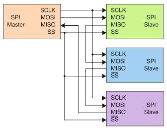
THIS CHAPTER DESCRIBES HOW DAISY CHAIN CONFIGURATION WORKS
In Daisy chain SPI interface; command propagates from one device to another, connected in
serial.
Figure below shows device connected in daisy chain configuration.
Figure 1-1: Micro controller with Daisy chain slaves
Active low slave select signal and SCLK are connected to all devices. Only the first slave in
the chain receives the command data directly from the microcontroller. Every other slave in
the network receives its MOSI data from the MISO output of the preceding slave in the
chain.
The SPI port of each slave is designed to send out during the second group of clock pulses
an exact copy of what it received during the first group of clock pulses. The whole chain acts
as an SPI communication shift register.
Figure below shows command sequence if we want to send data 0x9ABC to Slave 1, data
0x5678 to Slave 2 and data 0x1234 to Slave 3.
MCU-AN-300101-E-V10 -6- © Fujitsu Microelectronics Europe GmbH-10SPI - DAISY CHAIN COMMUNICATION
Chapter 1 Daisy Chain Configuration
Figure 1-2: Command Sequence
During the first command cycle (set of 16 SCLK pulses), 0x1234 gets loaded in the shift
register of Slave 1. With active-low slave select remaining low, this data propagates through
Slave1 and is output at MISO1 during the next command cycle. During this second
command cycle, the data from MISO1 moves directly into MOSI2, and 0x1234 is loaded into
Slave 2's shift register. Simultaneously, a new command, 0x5678, gets loaded into Slave 1’s
shift register, thus overwriting its previous command.
In the third command cycle, the first command, 0x1234, is loaded into Slave 3's shift
register. The second command, 0x5637, gets loaded into Slave 2, and Slave 1 receives a
new command, 0x9ABC. All three Slaves now have a command, which they received
through the daisy-chain in their shift registers. When active-low Slave select goes high, the
loaded command is executed.
© Fujitsu Microelectronics Europe GmbH -7- MCU-AN-300101-E-V10SPI - DAISY CHAIN COMMUNICATION
Chapter 2 Daisy Chain peripheral
2 Daisy Chain peripheral
THIS CHAPTER DESCRIBES HOW TO COMMUNICATE WITH SPI – DAISY CHAIN
PHERIPERAL
2.1 Digital to Analog Converter
MAX5232/33 is dual 10-bit voltage output Digital to Analog converter. It works on single 5V
supply and has internal reference voltage at 2.465V and features full scale output of 4.092V.
The MAX5232/33 has the following pin-out:
Figure 2-1 Pin Diagram MAX5232/33
PIN Name Function
1 OSA DAC A Offset Adjust
2 OUTA DAC A Output
3 RSTV Reset Value Input
1: Connect to VDD to select mid scale as the reset value.
0: Connect to DGND to select zero as the reset value.
4 LDACX Load DACs A and B
5 CLRX Clear Input. Both DAC outputs go to zero or mid scale. Clears both DAC
internal registers (input register and DAC register) to its predetermined
(RSTV) state.
6 CSX Chip-Select Input
7 DIN Serial Data Input. Data is clocked in on the rising edge of SCLK.
8 SCLK Serial Clock Input
9 DGND Digital Ground
10 DOUT Serial Data Output
11 PDLX Power-Down Lockout. Disables shutdown of both DACs when low.
12 REF Reference Output. Reference provides a 2.465V (MAX5233) or 1.234V
(MAX5232) nominal output.
13 AGND Analog Ground
14 VDD Positive Power Supply. Bypass VDD with a 0.1µF capacitor in parallel with a
4.7µF capacitor to AGND, and bypass VDD with a 0.1µF capacitor to DGND.
MCU-AN-300101-E-V10 -8- © Fujitsu Microelectronics Europe GmbH-10SPI - DAISY CHAIN COMMUNICATION
Chapter 2 Daisy Chain peripheral
15 OUTB DAC B Output
16 OSB DAC B Offset Adjust
Table 2-1: MAX5232/33 Pin Description
2.1.1 Connection to MB91467D
The DAC can be connected as shown in the following schematic. Please note that no power
supply pins and other MCU-Pins are drawn than those for the connection to the DAC.
Figure 2-2: Connections between MAX5232/33 and MB91467D
Apart from this, RSTV pin of all DACs are connected to ground to select zero as the reset
value. PDLX pin is connected to ground to disables shutdown of both DACs when low.
2.1.2 Communication Timing
Detailed description of the timing and timing parameters can be found in the corresponding
datasheet of the MAX5232/33 DAC.
Figure 2-3: Write Cycle
Above figure shows the timing for the serial interface. The serial word consists of 3 control
bits followed by 10 data bits (MSB first) and 1 sub-bit as described in the command table
shown below. When the three control bits are all zeros or all 1, D9–D6 are used as additional
control bits, allowing for greater DAC functionality.
The digital inputs allow any of the following
• Loading the input register(s) without updating the DAC register(s),
• Updating the DAC register(s) from the input register(s),
• Updating the input and DAC register(s) simultaneously.
The control bits and D9–D6 allow the DACs to operate independently.
© Fujitsu Microelectronics Europe GmbH -9- MCU-AN-300101-E-V10SPI - DAISY CHAIN COMMUNICATION
Chapter 2 Daisy Chain peripheral
The control bits and D9–D6 determine which registers update and the state of the registers
when exiting shutdown.
The 3-bit control and D9–D6 determine the following
• Registers to be updated
• Selection of the power-down and shutdown modes
The general timing diagram of Figure 2.3 illustrates data acquisition. Driving CSX low
enables the device to receive data. Otherwise the interface control circuitry is disabled. With
CS low, data at DIN is clocked into the register on the rising edge of SCLK. As CSX goes
high, data is latched into the input and/or DAC registers, depending on the control bits and
D9–D6. The maximum clock frequency guaranteed for proper operation is 13.5MHz.
2.1.3 Used DAC Commands
The following commands are used in the code example below:
16 Bit SERIAL WORD
FUNCTION
C2 C1 C0 D9 to D0 S2-S0
0 0 1 10-bit DAC data 000 Load input register A; DAC registers are
unchanged
0 1 0 10-bit DAC data 000 Load input register A; all DAC registers are
updated.
0 1 1 10-bit DAC data 000 Load all DAC registers from the shift register
(start up both DACs with new data, and load
the input registers).
1 0 0 XXXXXXXXXX 000 Update both DAC registers from their
respective input registers (start up both
DACs with data previously stored in the input
registers).
1 0 1 10-bit DAC data 000 Load input registers B; DAC registers are
unchanged.
1 1 0 10-bit DAC data 000 Load input registers B; all DAC registers are
updated.
1 1 1 P1A P1B X X X X X X X X 000 Shut down both DACs, respectively;
according to bits P1A and P1B (see Table
2.6). Internal bias and reference remain
active.
0 0 0 001XXXXXXX 000 Update DAC registers A from input register
A (start up DAC A with data previously
stored in input register A).
0 0 0 0 1 1 P1A P1B X X X X X 000 Full Power-Down. Power down the main bias
generator and shut down both DACs,
respectively, according to bits P1A and P1B
(see Table 2.6).
0 0 0 101XXXXXXX 000 Update DAC registers B from input register
B (start up DAC B with data previously
stored in input register B).
0 0 0 1 1 0 P1A X X X X X X 000 Shut down DAC A according to bit P1A (see
Table 2.6).
0 0 0 1 1 1 P1B X X X X X X 000 Shut down DAC B according to bit P1B (see
Table 2.6).
0 0 0 1000XXXXXX 000 Mode 0. DOUT clocked out on SCLK falling
edge (default).
0 0 0 1001XXXXXX 000 Mode 1. DOUT clocked out on SCLK rising
edge.
Table 2-2: MAX5232/33 Commands
MCU-AN-300101-E-V10 - 10 - © Fujitsu Microelectronics Europe GmbH-10SPI - DAISY CHAIN COMMUNICATION
Chapter 2 Daisy Chain peripheral
P1(A/B) SHUTDOWN MODE
0 Shut down with internal 1kK load to GND
1 Shut down with internal 200kK load to GND
Table 2-3: P1 Shutdown Modes
2.1.4 Example Code
The following code shows how to establish a communication with DAC.
For MAX5232/33 we need to transmit 2 bytes, hence if we connect 2 devices as per SPI
Daisy chain connection than in total we need to transmit 4 bytes.
Data transmitted to Device1
Stream of 4 bytes
NOP is transmitted to Device2
Figure 2-4: MAX5232/33 communication example
In function, parameter start refers to the position of first byte to be inserted in the stream of
MAX_BYTE stream.
© Fujitsu Microelectronics Europe GmbH - 11 - MCU-AN-300101-E-V10SPI - DAISY CHAIN COMMUNICATION
Chapter 2 Daisy Chain peripheral
/* THIS SAMPLE CODE IS PROVIDED AS IS AND IS SUBJECT TO ALTERATIONS. */
/* FUJITSU MICROELECTRONICS ACCEPTS NO RESPONSIBILITY OR LIABILITY */
/* FOR ANY ERRORS OR ELIGIBILITY FOR ANY PURPOSES. */
/* (C) Fujitsu Microelectronics Europe GmbH */
/*------------------------------------------------------------------------*/
#define MAX_BYTE 4 // n * 2 -> n = number of device in series
void max5232_write_mode(unsigned char start, unsigned char mode)
{
unsigned char count;
if (device> MAX_BYTE)
{
printf("MAX5232 Param Error!\r\n");
return;
}
spi_cs_enable() ;
for(count=1;count DOUT clocked out on SCLK falling edge
// mode : b’0 0 0 1 0 0 1 X -> DOUT clocked out on SCLK rising edge
// mode : b’0 0 0 1 1 0 P1A X -> Shut down DAC A according to bit P1A
// mode : b’0 0 0 1 1 1 P1B X -> Shut down DAC B according to bit P1B
// mode : b’1 1 1 P1A P1B X X -> Shut down both DACs, respectively
spi_tx_8Bit(mode);
spi_tx_8Bit(0x00);
count++;
}
else
{
spi_tx_8Bit(0x00);
}
}
spi_cs_disable() ;
}
In function, parameter start refers to the position of first byte to be inserted in the stream of
MAX_BYTE stream. Parameter cmd is to transmit command bits; the structure of it is as
described below
C2 C1 C0 0 0 0 0 0
Parameter data is the 10 bit Digital data which will be converted into analog value.
MCU-AN-300101-E-V10 - 12 - © Fujitsu Microelectronics Europe GmbH-10SPI - DAISY CHAIN COMMUNICATION
Chapter 2 Daisy Chain peripheral
/* THIS SAMPLE CODE IS PROVIDED AS IS AND IS SUBJECT TO ALTERATIONS. */
/* FUJITSU MICROELECTRONICS ACCEPTS NO RESPONSIBILITY OR LIABILITY */
/* FOR ANY ERRORS OR ELIGIBILITY FOR ANY PURPOSES. */
/* (C) Fujitsu Microelectronics Europe GmbH */
/*------------------------------------------------------------------------*/
#define MAX_BYTE 6 // = n * 2, n -> number of device connected in series
void max5232_load_reg(unsigned char start, unsigned char cmd,
unsigned short int data)
{
unsigned char count;
unsigned char datah = 0;
unsigned char datal = 0;
if ((start> MAX_DEVICE) || (data > 0x03FF))
{
printf("MAX5232 Param Error!\r\n");
return;
}
datah = (unsigned char )(data >> 5);
datal = (unsigned char )(data & 0x001F);
datah = cmd | datah ;
datal = datalSPI - DAISY CHAIN COMMUNICATION
Chapter 2 Daisy Chain peripheral
2.2 Digital potentiometer
The DS1806 Digital Sextet Potentiometer is a six-channel, digitally controlled, solid-state
linear potentiometer.
Each wiper’s position is selected via an 8-bit register value. Communication and control of
the device is accomplished via a 3-wire serial port interface.
The RSTX signal (3-wire serial port) is active when in a high state. Any communication
intended to change wiper settings must begin with the transition of the RSTX from the low
state to the high state. Once RSTX has transitioned from the low to the high state, the serial
port becomes active. When active, data is loaded into the I/O shift register on the low-to-high
transition of the CLK. DIN and CLK inputs are ignored when RSTX is in the low state.
The CLK signal input is used to provide timing synchronization for data input and output.
Wiper position data is loaded into the DS1806 through the DIN input terminal. This data is
shifted one bit at a time into the 48-bit I/O shift register of the part, LSB first.
As a data bit is entered into the I/O shift register of the DS1806, a bit will appear at the
COUT terminal before a maximum delay of 50 nanoseconds. The LSB of potentiometer-1
will always be the first out of the part at the beginning of a transaction. Additionally, the
COUT terminal is always active regardless of the state RSTX.
The COUT output of the DS1806 can be used to drive the DIN input of another DS1806. The
total number of bits transmitted is always 48 multiplied by the total number of DS1806s being
cascaded, when cascading multiple devices. For more information refer data sheet of
DS1806
The DL1806 has the following pin-out:
Figure 2-5 Pin Diagram DS1806
PIN Name Function
20 VCC 3V or 5V Supply
8 RSTX Serial Port Reset Input
12 DIN Serial Port Data Input
9 CLK Serial Port Clock Input
11 COUT Cascade Data Output
19-15,13 H1 to H6 High End terminal of Pot
1,2,4,5,7,17 W1 to W6 Wiper Terminal of Pot
10 GND Ground
3 L1-L3 Low Terminal Pots 1 through 3
6 L4-L6 Low Terminal Pots 4 through 6
Table 2-4: DL1806 Pin Description
MCU-AN-300101-E-V10 - 14 - © Fujitsu Microelectronics Europe GmbH-10SPI - DAISY CHAIN COMMUNICATION
Chapter 2 Daisy Chain peripheral
2.2.1 Connection to MB91467D
The Digital potentiometer can be connected as shown in the following schematic. Please
note that no power supply pins and other MCU-Pins are drawn than those for the connection
to the DAC.
Figure 2-6: Connections between DL1806 and MB91467D
2.2.2 Used Digital Potentiometer Commands
The following commands are used in the code example below:
8 bit Load VALUE
Function
B7 B6 B5 to B0
0 0 XXXXXXX Do not Load wiper value
0 1 XXXXXXX Load wiper value
1 0 XXXXXXX Load wiper value
1 1 XXXXXXX Load wiper value
Table 2-5: DL1806 Commands
© Fujitsu Microelectronics Europe GmbH - 15 - MCU-AN-300101-E-V10SPI - DAISY CHAIN COMMUNICATION
Chapter 2 Daisy Chain peripheral
2.2.3 Example Code
The following code shows how to establish a communication with DAC.
For DS1806 we need to transmit 6 bytes, hence if we connect 2 devices as per SPI Daisy
chain connection than in total we need to transmit 12 bytes.
Data transmitted to Device1 Stream of 12 bytes
Dummy byte is transmitted to Device2
Figure 2-7: DS1806 communication example
/* THIS SAMPLE CODE IS PROVIDED AS IS AND IS SUBJECT TO ALTERATIONS. */
/* FUJITSU MICROELECTRONICS ACCEPTS NO RESPONSIBILITY OR LIABILITY */
/* FOR ANY ERRORS OR ELIGIBILITY FOR ANY PURPOSES. */
/* (C) Fujitsu Microelectronics Europe GmbH */
/*------------------------------------------------------------------------*/
#define MAX_BYTE 12 // = n * 6, n -> number of devices connected in series
void DS1806_write_wiper_setting(unsigned char start, unsigned char pot_no,
unsigned char wiper_position)
{
unsigned char pot_count;
if ((start> MAX_BYTE) ||(pot_no>MAX_POT) || (wiper_position > 0x3F))
{
printf("DS1806 Param Error!\r\n");
return;
}
spi_cs_enable() ;
for(count=1;countSPI - DAISY CHAIN COMMUNICATION
Chapter 2 Daisy Chain peripheral
In function, parameter start refers to the position of first byte to be inserted in the stream of
MAX_BYTE (12 bytes) stream. There are 6 potentiometer inside DS1806, parameter
pot_no refers to the potentiometer for which we want to set wiper setting. Byte 0xFF is
transmitted for wiper setting of other potentiometers with first two MSB bits set, wiper setting
of other potentiometers of the same device or those of other device is not changed.
© Fujitsu Microelectronics Europe GmbH - 17 - MCU-AN-300101-E-V10SPI - DAISY CHAIN COMMUNICATION
Chapter 3 APPENDIX A
3 APPENDIX A
THIS CHAPTER NAMES THE RELATED DOCUMENTS
3.1 Related Documents
• mcu-an-300002-e-spi Fujitsu Application Note about SPI Modes
• MAX5232/33 Maxim data sheet for MAX5232/33
• DS1806 Dallas data sheet for DS1806
MCU-AN-300101-E-V10 - 18 - © Fujitsu Microelectronics Europe GmbH-10SPI - DAISY CHAIN COMMUNICATION
Chapter 4 Additional Information
4 Additional Information
Information about FUJITSU Microcontrollers can be found on the following Internet page:
http://mcu.emea.fujitsu.com/
The software example related to this application note is:
91460_uart_spi_master_DaisyChain_max5233
91460_uart_spi_master_DaisyChain_DS1806
It can be found on the following Internet page:
http://mcu.emea.fujitsu.com/mcu_product/mcu_all_software.htm
© Fujitsu Microelectronics Europe GmbH - 19 - MCU-AN-300101-E-V10SPI - DAISY CHAIN COMMUNICATION
List of Figures
List of Figures
Figure 1-1: Micro controller with Daisy chain slaves............................................................... 6
Figure 1-2: Command Sequence ........................................................................................... 7
Figure 2-1 Pin Diagram MAX5232/33..................................................................................... 8
Figure 2-2: Connections between MAX5232/33 and MB91467D............................................ 9
Figure 2-3: Write Cycle .......................................................................................................... 9
Figure 2-4: MAX5232/33 communication example ............................................................... 11
Figure 2-5 Pin Diagram DS1806 .......................................................................................... 14
Figure 2-6: Connections between DL1806 and MB91467D.................................................. 15
Figure 2-7: DS1806 communication example....................................................................... 16
MCU-AN-300101-E-V10 - 20 - © Fujitsu Microelectronics Europe GmbH-10SPI - DAISY CHAIN COMMUNICATION
List of Tables
List of Tables
Table 2-1: MAX5232/33 Pin Description ................................................................................ 9
Table 2-2: MAX5232/33 Commands .................................................................................... 10
Table 2-3: P1 Shutdown Modes ........................................................................................... 11
Table 2-4: DL1806 Pin Description....................................................................................... 14
Table 2-5: DL1806 Commands ............................................................................................ 15
© Fujitsu Microelectronics Europe GmbH - 21 - MCU-AN-300101-E-V10You can also read