High-performance coherent optical modulators based on thin-film lithium niobate platform - Nature
←
→
Page content transcription
If your browser does not render page correctly, please read the page content below
ARTICLE
                   https://doi.org/10.1038/s41467-020-17806-0                OPEN

                  High-performance coherent optical modulators
                  based on thin-film lithium niobate platform
                  Mengyue Xu 1, Mingbo He1, Hongguang Zhang2,3, Jian Jian1, Ying Pan1, Xiaoyue Liu 1, Lifeng Chen                                               1,

                  Xiangyu Meng1, Hui Chen1, Zhaohui Li1, Xi Xiao 2,3 ✉, Shaohua Yu2,3, Siyuan Yu1 & Xinlun Cai 1 ✉
1234567890():,;

                  The coherent transmission technology using digital signal processing and advanced mod-
                  ulation formats, is bringing networks closer to the theoretical capacity limit of optical fibres,
                  the Shannon limit. The in-phase/quadrature electro-optic modulator that encodes informa-
                  tion on both the amplitude and the phase of light, is one of the underpinning devices for the
                  coherent transmission technology. Ideally, such modulator should feature a low loss, low
                  drive voltage, large bandwidth, low chirp and compact footprint. However, these require-
                  ments have been only met on separate occasions. Here, we demonstrate integrated thin-film
                  lithium niobate in-phase/quadrature modulators that fulfil these requirements simulta-
                  neously. The presented devices exhibit greatly improved overall performance (half-wave
                  voltage, bandwidth and optical loss) over traditional lithium niobate counterparts, and sup-
                  port modulation data rate up to 320 Gbit s−1. Our devices pave new routes for future high-
                  speed, energy-efficient, and cost-effective communication networks.

                  1 State
                        Key Laboratory of Optoelectronic Materials and Technologies and School of Electronics and Information Technology, Sun Yat-sen University, 510006
                  Guangzhou, China. 2 National Information Optoelectronics Innovation Center, China Information and Communication Technologies Group Corporation
                  (CICT), 430074 Wuhan, China. 3 State Key Laboratory of Optical Communication Technologies and Networks, China Information and Communication
                  Technologies Group Corporation (CICT), 430074 Wuhan, China. ✉email: xxiao@wri.com.cn; caixlun5@mail.sysu.edu.cn

                  NATURE COMMUNICATIONS | (2020)11:3911 | https://doi.org/10.1038/s41467-020-17806-0 | www.nature.com/naturecommunications                            1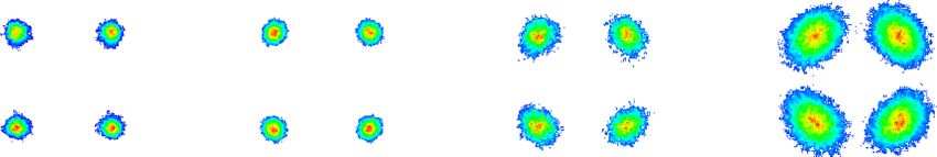
ARTICLE NATURE COMMUNICATIONS | https://doi.org/10.1038/s41467-020-17806-0
O
ver decades and across all levels of optical networks, the ground–signal–ground (GSG) microelectrodes, where the two LN
global internet traffic has experienced continuous growth arms lie in the gaps of the ground and signal electrodes. (Fig. 1b)
at an enormous rate1,2. To keep up with this ever- The device operates in a single-drive push–pull configuration, so
increasing demand, the digital coherent transmission technology that applied microwave fields induce phase shifts with an equal
has been introduced for long-haul communication links and is magnitude but opposite sign in both arms, leading to nearly
allowing networks to approach the maximum achievable capacity chirp-free modulation. Two thermo-optic (TO) phase shifters
of optical fibres, known as the Shannon limit3–7. This technology (DC1 and DC2) are employed to control the modulation bias
is now expected to penetrate into the rapidly growing, capacity- points of the I and Q branches independently. (Fig. 1c) For QPSK
hungry short reach links, such as metro and data-centre inter- and QAM modulation, the bias points need to be set at null
connects, where an in-phase/quadrature (IQ) modulator must be points. A third TO phase shifter (DC3) introduces a static π/2
operated in a small space, while featuring low loss, low drive phase shift between the modulated signals from the two sub-
voltages, and large bandwidths8–10. For nearly a decade, IQ MZMs, which puts them in quadrature to each other. To couple
modulators based on low-index-contrast lithium niobate light in and out of the device, amorphous silicon/LN hybrid
(LiNbO3, LN) waveguides have been the mainstay for generating grating couplers are used for transverse-electric (TE) mode
the advanced modulation formats11–14. Although these mod- coupling47.
ulators have enjoyed tremendous success in long-haul coherent The cross-section of the LN waveguides, together with the
networks, their performance is already reaching a limit because travelling-wave electrodes, are optimised to achieve a low Vπ and
the low-index-contrast LN waveguides cannot support them. To a large EO bandwidth simultaneously. The LN waveguides in the
date, the off-the-shelf LN-based IQ modulators are still bulky and phase modulation sections have a top width w of 4 μm, a slab
power-consuming with a moderate half-wave voltage (Vπ) of thickness s of 300 nm and a rib height h of 300 nm. The sidewall
3.5 V requiring devices of at least 5 cm, and with little hope for of the waveguide is tilted with an angle of 64° (Fig. 1d). The
further improving the electric–optic (EO) bandwidth (typically lithography and etching processes were optimised to achieve
around 35 GHz), which limits their practical short reach smooth sidewalls, which was confirmed by atomic force
applications. microscope (AFM) measurements (see Supplementary Note 3
Tremendous efforts have been made to realise small-footprint and Supplementary Fig. 3). The propagation loss of single-mode
and high-performance IQ modulators in various material plat- and 4-um-wide LN waveguides were measured to be 0.3 dB cm−1
forms, including silicon (Si), indium phosphide (InP), polymers, and 0.15 dB cm−1, respectively (see Supplementary Fig. 4). The
and plasmonics15–32. Although these platforms normally offer the gap between the LN waveguides and electrodes was set to 1.5 μm.
advantages of compact footprints and large bandwidths, each type These parameters are devised carefully to balance the trade-off
of modulator has its limitations, including large Vπ (Si), high between the voltage-length product (VπL) and bandwidth-voltage
optical loss (plasmonics), nonlinear response (InP), or doubts ratio (BW/Vπ), which are two key figures of merit of optical
over long-term stability (polymer). The development of an ideal modulators (see Supplementary Note 4 and Supplementary
IQ modulator that possesses all the desired characteristics Fig. 5). The coplanar travelling-wave electrodes are designed to
simultaneously remains a challenge, mainly due to limitations simultaneously achieve broadband impedance matching, as well
from underlying materials. as velocity matching of the microwave and optical signals. The
LN-on-insulator (LNOI) has recently emerged as an appealing thickness of the electrodes t was set to 900 nm; the gaps between
material platform for compact and high-performance mod- the signal and ground electrodes were set to 7 μm, and the widths
ulators, on which high-contrast waveguides with strong optical of the signal ws and ground wg electrodes were set to 19.5 and 80
confinement can be formed by simply etching the device layer of μm, respectively (Fig. 1e).
an LNOI wafer33–46. This approach unlocks new levels of per-
formance and scales in LN modulators because it overcomes the
fundamental voltage-bandwidth-size trade-off in conventional Device characteristics. The fabricated LNOI IQ modulators with
low-index-contrast LN modulators. Recently, LNOI-based arm lengths of 7.5 mm and 13 mm are measured in detail. We
Mach–Zehnder modulators (MZMs) with low drive voltages first measured the direct current transmission with TO phase
and ultrahigh EO bandwidths, which significantly outperform shifters. Figure 2a shows the TO transmission curve as a function
their conventional counterparts, have been demonstrated (see of the applied voltage. The length of the TO phase shifter is only
Supplementary Note 1). 160 μm with a resistance of 760 Ω, and the required voltages for
Here, we demonstrate the IQ modulator based on the LNOI biasing at quadrature and null are 3.55 and 7.2 V, corresponding
platform, which is capable of encoding signals with advanced to power dissipations of 16.6 and 68.2 mW, respectively. Instead
modulation formats, such as quadrature phase-shift keying (QPSK) of the EO effect, the TO effect is used here for DC bias voltage
and quadrature amplitude modulation (QAM) signals. The pro- control, offering two distinct advantages. First, the TO effect is
posed device features low optical loss, low Vπ, ultrahigh EO much stronger compared to the EO effect, allowing for much
bandwidth, and much smaller footprint than the conventional LN compact device size. In our case, the length of the EO phase
counterpart. Furthermore, QPSK modulation up to 220 Gbit s−1 shifter would have been more than 5 mm for the same amount of
(110 Gbaud), and 16 QAM modulation up to 320 Gbit s−1 voltage. Second, LN is well-known for its drifts in the DC bias
(80 Gbaud), are successfully demonstrated. point upon the application of a static electric field, which is a
phenomenon that originates from the piezoelectric nature of the
material11,48,49. This drift must be compensated by a fast feedback
Results loop for practical use. This phenomenon is absent in TO phase
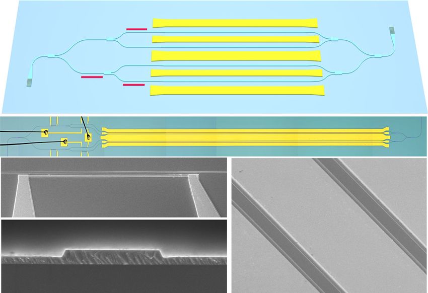
Device design. Figure 1a illustrates the schematic of the proposed shifters, and a much simpler control scheme could be used
device. The LNOI-based IQ modulator is constructed by nesting instead. To provide a comparative study, we record the output
two parallel travelling-wave MZMs as I and Q components, power from an LNOI MZM biased at quadrature using both TO
respectively. The optical power splitters/combiners are imple- and EO phase shifters. Figure 2b shows the measured results in
mented by 1 × 2 multimode interference (MMI) couplers (see 30 min, confirming that the DC bias point with the TO effect is
Supplementary Note 2, Supplementary Figs. 1 and 2). Both I and much more stable than with the EO effect. It should be noted that
Q MZMs are balanced travelling-wave modulators with the TO phase shifter consumes static power, while EO phase
2 NATURE COMMUNICATIONS | (2020)11:3911 | https://doi.org/10.1038/s41467-020-17806-0 | www.nature.com/naturecommunicationsNATURE COMMUNICATIONS | https://doi.org/10.1038/s41467-020-17806-0 ARTICLE
a
DC1 G Grating coupler
In-phase branch S
MMI
G
Quadrature branch S
DC3
DC2 G
b
1 mm
c e
Thermo-optic phase shifter
(Titanium) 20 μm
d
1 μm 10 μm
300 nm 600 nm
Fig. 1 IQ modulator on the LNOI platform. a Schematic of an LNOI-based IQ modulator. b Microscope image of the fabricated chip. c Scanning electron
microscopy (SEM) image of the thermos-optic phase shifter. d SEM image of the cross-section of the LN waveguides. e SEM image the gold electrodes and
the LN waveguides.
a 1 b
3
0.8
0
Power shift (dB)
Transmission
0.6 Quadrature
–3 Electrical bias
Thermal bias
0.4 –6
0.2 –9
Null
0 –12
0 50 100 150 200 0 10 20 30
Power (mW) Time (min)
Fig. 2 TO phase shifters performance. a TO transmission curve as a function of the power dissipations. b Power shift from an MZM biased at quadrature
using EO (green line) and TO (blue line) phase shifters as a function of the operating time.
shifter does not. We also fabricated an IQ modulator with EO the measurement limit of our vector network analyser (VNA).
phase shifters for further comparison (Supplementary Note 5, These voltage and bandwidth parameters indicate a much better
Supplementary Fig. 6 and Supplementary Table 1). performance over conventional LN modulators and are well
Next, we measured the Vπ for both devices with 100 kHz suited for high-speed operation beyond 100 Gbaud. The input
triangular voltage sweeps. The measured Vπ for the 7.5 and 13 return losses (S11 parameter) of both devices are less than −18 dB
mm devices are 3.1 and 1.9 V, corresponding to VπL of 2.3 and at up to 67 GHz, which are small enough for practical use
2.4 V cm, respectively (Fig. 3a, b). The inset of Fig. 3a shows the (Fig. 4b).
transmission of one of the sub-MZMs on a logarithmic scale, The fibre-to-fibre insertion losses at peak transmission are
indicating a measured extinction ratio of >25 dB. We have measured to be 8.6 dB and 8.25 dB for 13 mm and 7.5 mm device,
fabricated more than ten devices on the same chip, and the respectively. The coupling loss of the grating couplers is 3.4 dB/
measured extinction ratios are between 24 and 28 dB. Figure 3b facet. Therefore, the on-chip losses are 1.8 dB and 1.45 dB for
shows the optical transmission at different wavelengths, showing 13 mm and 7.5 mm device, respectively. The coupling loss can be
broadband operation in the whole C-band. further improved by replacing grating coupler with edge-coupled
We then characterised the small-signal EO bandwidth (S21 spot-size converters, with fibre-to-fibre losses below 4 dB
parameter) and electrical reflections (S11) of the fabricated practically achievable.
devices. For the 13-mm device, the measured 3-dB EO
bandwidths of both I and Q MZMs are greater than 48 GHz Data modulation. We use our low-Vπ, large-bandwidth, and low-
with a reference frequency of 1.5 GHz. For the 7.5-mm device, the loss 13-mm LNOI IQ modulators to generate advanced mod-
EO bandwidth is greater than 67 GHz (Fig. 4a), which is beyond ulation formats of up to 320 Gb s−1. The experimental setup is
NATURE COMMUNICATIONS | (2020)11:3911 | https://doi.org/10.1038/s41467-020-17806-0 | www.nature.com/naturecommunications 3ARTICLE NATURE COMMUNICATIONS | https://doi.org/10.1038/s41467-020-17806-0
a 1 b 1
I-branch I-branch
0.8 Q-branch 0.8 Device L = 7.5 mm Q-branch
Vπ = 1.9 V
Transmission
Transmission
0.6 0.6
Transmission (dB)
0
Device L = 13 mm
0.4 –10 0.4
Vπ = 3.1 V
–20
0.2 ER > 25 dB 0.2
–30
0 0
–2 –1 0 1 2 –5 –4 –3 –2 –1 0 1 2 3 4 5
Voltage (V) Voltage (V)
c 1
0.8 1530 nm
Transmission
1550 nm
0.6 1570 nm
0.4
0.2
0
–2 –1.5 –1 –0.5 0 0.5 1 1.5 2
Volatge (V)
Fig. 3 Static EO characteristics. a, b Normalised optical transmission of both branches of the 13-mm and 7.5-mm devices as a function of the applied
voltage, showing Vπ of 1.9 V and 3.1 V, respectively. The inset of a shows the measured normalised transmission on a logarithmic scale, showing an
extinction ratio greater than 25 dB. c Measured optical transmission at different wavelengths.
a b 0
I-branch I-branch
0 7.5 mm Q-branch Q-branch
–10
Electro-electro S11 (dB)
Electro-optic S21 (dB)
–18 dB
–2 –20
13 mm
–3 dB ~ 48 GHz
–4 –30
–6 –40
–6 dB
–8 –50
10 20 30 40 50 60 70 10 20 30 40 50 60 70
Frequency (GHz) Frequency (GHz)
Fig. 4 Small-signal response. a EO bandwidths (S21 parameter) and b electrical reflection S11 of the 13-mm IQ modulator.
shown in Fig. 5a. First, we demonstrate the generation of QPSK, 60 Gbaud 16 QAM, shown in Fig. 5h. The BERs are also well
one of the most widely deployed formats in coherent transmis- below the SD-FEC limit and no error floor can be observed in the
sion systems, for performance benchmarking. Figure 5b–e sum- measurement. The high SNR demonstrated here benefits from a
marises the measured constellation diagrams at 60, 80, 100, and combination of linear EO response, low insertion loss and pure
110 Gbaud, corresponding to data-transmission rates of 120, 160, phase modulation, all of which are derived from the Pockels effect
200, and 220 Gb s−1, respectively. All the modulated QPSK sig- in the LN material.
nals yield very good bit error rate (BER) performance well below
the KP4 forward error correction (FEC) limit of 2 × 10⁻⁴. Discussion
Moreover, error-free operations at 80 and 100 Gbaud were As presented above, the reported IQ modulator demonstrates
achieved with BER < 1 × 10⁻⁹. We then use 16 QAM modulation ultrahigh speed and high-signal fidelity when encoding infor-
formats at high baud rate to further increase the data rates and mation into the amplitude and phase of the light. As far as we are
investigate the signal-to-noise ratio (SNR), a common measure aware, this is the first reported successful demonstration of IQ
for the fidelity of modulated signals. The constellation diagrams modulators based on LNOI platforms. The overall performance
at 60 and 80 Gbaud with QAM are shown in Fig. 5f, g. With the of optical modulators in terms of voltage, bandwidth, and foot-
60 Gbaud 16 QAM (data rate of 240 Gbit s−1), we can achieve a print can be evaluated by two figures of merit: the VπL and
low BER of 8.6 × 10⁻⁵. With the 80 Gbaud 16 QAM (data rate of BW/Vπ. The present device exhibits VπL and BW/Vπ of around
320 Gbit s−1), the measured BER of 8.4 × 10⁻³ is still within 2.5 V cm and 25 GHz V−1, significantly outperforming conven-
the tolerance of the soft-decision forward error correction (SD- tional LN counterparts. The overall length of the present device is
FEC) limit of 4 × 10⁻². The back-to-back (B2B) BER curves at ~15 mm, which is small enough to fit into compact coherent
4 NATURE COMMUNICATIONS | (2020)11:3911 | https://doi.org/10.1038/s41467-020-17806-0 | www.nature.com/naturecommunicationsNATURE COMMUNICATIONS | https://doi.org/10.1038/s41467-020-17806-0 ARTICLE
a Real-time oscilloscope
G DC1
PC S
AWG
G
120 Gsa/s S
Tunable DC3
laser G DC2
RF Amp. Signal LO
OMA
b 60 Gbaud QPSK c 80 Gbaud QPSK d 100 Gbaud QPSK e 110 Gbaud QPSK
BER = 2.52 × 10–55 BER = 1.56 × 10⁻²⁵ BER = 4.67 × 10⁻¹⁰ BER = 8.63 × 10⁻⁶
h 10–1
f 60 Gbaud 16QAM g 80 Gbaud 16QAM
SD-FEC
10–2
B2B BER
10–3
10–4 KP4-FEC
10–5 BER = 8.62 × 10⁻⁵ BER = 8.41 × 10⁻³
–15 –13 –11 –9 –7 –5
Received optical power (dB)
Fig. 5 Data modulation testing. a Experimental setup for coherent data transmission. AWG: arbitrary waveform generator, LO: local oscillator, OMA:
optical modulation analyser, PC: polarisation controller. b–g Constellation diagram for QPSK signals with symbol rates of 60, 80, 100, and 110 Gbaud and
16 QAM signals with symbol rates of 60 and 80 Gbaud. h Measured curve of BER versus the received optical power for 60 Gbaud 16 QAM signal.
Table 1 Comparison of several performance metrics of IQ modulators.
Vπ (V) 3-dB EO bandwidth (GHz) Length of modulation area (mm) On-chip loss (dB) Data rate (Gb/s) (BER)
SOI19 7.5 32 4.5 6.8 360 (2 × 10⁻²)
InP16,17 1.5 67 ~3.6 ~2 448 (6.68 × 10⁻³)
InP18 1.7 43 4 7a 64
GaAs24 3 27 30 500 0.015c 11.2 400 (4.5 × 10⁻²)
Commercial LN51 3.5 35 30~80 NA 256
This work 1.9 ~48 13 1.8 320 (8.41 × 10⁻³)
3.1 >67 7.5 1.45
NA: not available.
aThis value was calculated from the 8 dB insertion loss and 1 dB loss in the spot-size converter.
bThis value was calculated from the 17.5 dB fibre-to-fibre loss and 9 dB off-chip coupling loss.
cThis value was calculated from the reported V L of 130 V μm and length of 15 μm.
π
transceiver packages, such as the CFP2-ACO (C-form factor the best InP modulators. Furthermore, in contrast to InP-based IQ
pluggable analogue coherent optics) and QSFP-DD (quad small modulators, in which thermoelectric cooling (TEC) is indis-
form factor pluggable double density). pensable for reliable operation, the LNOI-based IQ modulator
In Table 1, we compare the performance of the present device could be operated without TEC, which is highly desirable for low-
with the state-of-the-art, including commercial LN IQ modulators, cost applications. We believe that the EO bandwidth of the present
and IQ modulators based on silicon, InP, GaAs, silicon–organic- device could be further extended beyond 100 GHz without com-
hybrid (SOH) and plasmonics. Conventional LN IQ modulators promising the half-wave voltage, by further optimising the
are also included as a benchmark. Clearly, the present device travelling-wave electrode (see Supplementary Note 4). This could
features the best optical loss compared among the others, and to support data rates of over 200 Gbaud. By further integrating
the best of our knowledge, this is the lowest insertion loss ever on-chip polarisation combiners, a single LNOI-based modulator
achieved in IQ modulators. This characteristic makes the present could operate at a data rate of >1 Tb s−1 using, for example,
device suitable for applications in short reach links, where the 16 QAM modulation at 200 Gbaud. The demonstrated LNOI
optical power budget becomes critical owing to prohibitive platform could therefore lead to a paradigm shift in building
deployment of optical amplifiers. The Vπ and bandwidth of the compact and high-performance IQ modulators, offering a crucial
present device are also very appealing for high-speed and low- edge for future ultra-fast and low-power consumption optical fibre
power consumption operations, which are comparable to those of interconnects.
NATURE COMMUNICATIONS | (2020)11:3911 | https://doi.org/10.1038/s41467-020-17806-0 | www.nature.com/naturecommunications 5ARTICLE NATURE COMMUNICATIONS | https://doi.org/10.1038/s41467-020-17806-0
Methods 8. Saida, T. Emerging integrated devices for coherent transmission—digitally
Device fabrication. The devices were fabricated on a commercial X-cut LNOI assisted analog optics. In 2017 Optical Fiber Communications Conference and
wafer from NANOLN. We used electron-beam lithography (EBL) to define Exhibition (OFC) (IEEE, Los Angeles, 2017).
waveguide patterns after spinning Hydrogen silsesquioxane (HSQ). The 300-nm- 9. Ogiso, Y. et al. Ultra-high bandwidth InP IQ modulator co-assembled with
high ridges of the LN waveguides were formed in an optimised argon plasma in an driver IC for beyond 100-GBd CDM. In 2018 Optical Fiber Communication
inductively coupled plasma etching system. Afterwards, we deposited a 220-nm Conference (IEEE, San Diego, 2018).
amorphous-Si (a-Si) layer on the patterned LN waveguides and spin-coated HSQ 10. Doerr, C. Coherent optics in Si photonics. In 2018 Optical Fiber
on the a-Si for EBL. The Si/LN grating couplers were used for off-chip coupling. Communication Conference (IEEE, San Diego, 2018).
Then, we used a polymethyl methacrylate resist for a lift-off process to produce the 11. Chen, A. & Murphy, E. Broadband Optical Modulators: Science, Technology,
200-nm-thick TO phase shifters. Finally, 900-nm-thick gold travelling-wave elec- and Applications (CRC Press, USA, 2011).
trodes were patterned through a lift-off process. 12. Wooten, E. L. et al. A review of lithium niobate modulators for fiber-optic
communications systems. IEEE J. Sel. Top. Quantum Electron. 6, 69–82
High-speed data modulation. At the transmitter, the two independent RF signals (2000).
with a length of a pseudo-random bit sequence of 215–1 were generated from a 13. Raybon, G. et al. 180-GBaud All-ETDM single-carrier polarization
120-GSa/s arbitrary waveform generator (Keysight, M8194A). A root-raised-cosine multiplexed QPSK transmission over 4480 km. In 2018 Optical Fiber
filter was used for pulse shaping in the frequency domain. After being amplified by Communication Conference (IEEE, San Diego, 2018).
linear amplifiers (SHF S807C, 3 dB BW: 55 GHz), the output signals were fed into 14. Schuh, K. et al. Single carrier 1.2 Tbit/s transmission over 300 km with PM-64
the IQ modulator by an RF probe (ground–signal-ground–signal-ground (GSGSG) QAM at 100 GBaud. In 2017 Optical Fiber Communication Conference (IEEE,
configuration, 3 dB BW > 67 GHz). A second GSGSG RF probe was used to ter- Los Angeles, 2017).
minate the end of the transmission line with a 50-Ω load to avoid back-reflected 15. Going, R. et al. Multi-channel InP-based coherent PICs with hybrid integrated
signals. SiGe electronics operating up to 100 GBd, 32QAM. In European Conference
Light from a tunable laser (Santec TSL-550) with 17 dBm output power was on Optical Communication (IEEE, Gothenbug, 2017).
coupled into and collected from the chip via amorphous-Si/LN grating couplers. A 16. Ogiso, Y. et al. Over 67 GHz bandwidth and 1.5 V Vπ InP-based optical IQ
polarisation controller was used to ensure transverse-electric mode input. An modulator with n-i-p-n heterostructure. J. Lightwave Technol. 35, 1450–1455
optical modulation analyser (OMA, Keysight N4391B) with a four-channel real- (2017).
time oscilloscope (Keysight UXR0704A, 256 GSa/s) served as a receiver. The 17. Ogiso, Y. et al. Ultra-high bandwidth InP IQ modulator for beyond 100-GBd
modulated signal was received B2B and mixed with an internal local oscillator in transmission. In 2019 Optical Fiber Communication Conference (IEEE, San
the OMA. A series of digital signal processing steps, including low-pass filtering, Diego, 2019).
polarisation demultiplexing, and feed-forward compensation, were included in the 18. Lange, S. et al. Low power InP-based monolithic DFB-laser IQ modulator with
vector signal analysis (Keysight) software. The data decoded from the OMA were SiGe differential driver for 32-GBd QPSK modulation. J. Lightwave Technol.
used for BER and error vector magnitude (EVM) measurements. The EVM 34, 1678–1682 (2016).
describes the deviation of a measured symbol point from its ideal position in the
19. Lin, J., Sepehrian, H., Rusch, L. A. & Shi, W. Single-carrier 72 GBaud 32QAM
constellation diagram and can be used to reliably estimate the BER values assuming
and 84 GBaud 16QAM transmission using a SiP IQ modulator with joint
the signal is distorted by additive white Gaussian noise only50.
digital-optical pre-compensation. Opt. Express 27, 5610–5619 (2019).
20. Samani, A. et al. 180 Gb/s single carrier single polarization 16-QAM
Modulator energy considerations. For 16 QAM modulation, we can estimate the transmission using an O-band silicon photonic IQM. Opt. Express 27,
energy consumption per bit dissipated in the travelling-wave IQ modulator as 14447–14456 (2019).
Wbit,16QAM = 2 × Vrms2/(BR), where Vrms is the root-mean-square voltage of the 21. Goi, K. et al. Low-loss high-speed silicon IQ modulator for QPSK/DQPSK in
electrical PAM4 signal, B is the total bit rate and R is the equivalent resistor of C and L bands. Opt. Express 22, 10703–10709 (2014).
50 Ω. The value of Vrms applied to the one MZM was measured directly using the 22. Dong, P. et al. 112-Gb/s monolithic PDM-QPSK modulator in silicon. Opt.
oscilloscope. For 60 Gbaud 16 QAM (B = 240 Gbit s−1) modulation experiment Express 20, B624–B629 (2012).
with Vrms = 0.85 V, we can calculate an energy consumption of 120 fJ/bit. For 23. Dong, P. et al. Silicon in-Phase/quadrature modulator with on-chip optical
80 Gbaud 16 QAM (B = 320 Gbit s−1) modulation experiment with Vrms = 0.7 V, equalizer. J. Lightwave Technol. 33, 1191–1196 (2015).
we find a lower power consumption of 61 fJ/bit. To further reduce the energy 24. Schindler, P. C. et al. Monolithic GaAs electro-optic IQ modulator
consumption, we fabricated a LN MZM with a record low Vπ of 1.25 V while demonstrated at 150 Gbit/s with 64QAM. J. Lightwave Technol. 32, 760–765
maintaining a high modulation bandwidth (see Supplementary Note 6 and Sup- (2014).
plementary Fig. 7).
25. Lauermann, M. et al. Low-power silicon-organic hybrid (SOH) modulators for
advanced modulation formats. Opt. Express 22, 29927–29936 (2014).
Data availability 26. Korn, D. et al. Silicon-organic hybrid (SOH) IQ modulator using the linear
All the data supporting the findings in this study are available in the paper and electro-optic effect for transmitting 16QAM at 112 Gbit/s. Opt. Express 21,
Supplementary Information. Additional data related to this paper are available from the 13219–13227 (2013).
corresponding authors upon request. 27. Leuthold, J. et al. Silicon-organic hybrid electro-optical devices. IEEE J. Sel.
Top. Quantum Electron 19, 114–126 (2013).
28. Wolf, S. et al. Coherent modulation up to 100 GBd 16QAM using silicon-
Received: 2 January 2020; Accepted: 16 July 2020; organic hybrid (SOH) devices. Opt. Express 26, 220–232 (2018).
29. Haffner, C. et al. All-plasmonic Mach–Zehnder modulator enabling optical
high-speed communication at the microscale. Nat. Photon 9, 525–528 (2015).
30. Haffner, C. et al. Low-loss plasmon-assisted electro-optic modulator. Nature
556, 483–486 (2018).
31. Messner, A. et al. Plasmonic ferroelectric modulators. J. Lightwave Technol.
References 37, 281–290 (2019).
1. Cisco, I. Cisco visual Networking Index: Forecast and Methodology 2015–2020 32. Heni, W. et al. Plasmonic IQ modulators with attojoule per bit electrical
(Cisco, 2016). energy consumption. Nat. Commun. 10, 1694 (2019).
2. Winzer, P. J. & Neilson, D. T. From scaling disparities to integrated 33. Janner, D. et al. Micro-structured integrated electro-optic LiNbO3 modulators.
parallelism: a decathlon for a decade. J. Lightwave Technol. 35, 1099–1115 Laser Photon Rev. 3, 301–313 (2009).
(2017). 34. Poberaj, G., Hu, H., Sohler, W. & Günter, P. Lithium niobate on insulator
3. Kikuchi, K. Fundamentals of coherent optical fiber communications. J. (LNOI) for micro-photonic devices. Laser Photon Rev. 6, 488–503 (2012).
Lightwave Technol. 34, 157–179 (2016). 35. Guarino, A. et al. Electro–optically tunable microring resonators in lithium
4. Winzer, P. J. et al. Spectrally efficient long-haul optical networking using niobate. Nat. Photon 1, 407–410 (2007).
112-Gb/s polarization-multiplexed 16-QAM. J. Lightwave Technol. 28, 36. Jin, S., Xu, L., Zhang, H. & Li, Y. LiNbO3 Thin-film modulators using silicon
547–556 (2010). nitride surface ridge waveguides. IEEE Photonics Technol. Lett. 28, 736–739
5. Infinera Corporation. Coherent DWDM Technologies (Infinera Corporation, (2016).
2012). 37. Rao, A. et al. High-performance and linear thin-film lithium niobate
6. Raybon, G. et al. High symbol rate coherent optical transmission systems: 80 Mach–Zehnder modulators on silicon up to 50 GHz. Opt. Lett. 41, 5700–5703
and 107 Gbaud. J. Lightwave Technol. 32, 824–831 (2014). (2016).
7. Yamazaki, H., Sano, A., Nagatani, M. & Miyamoto, Y. Single-carrier 1-Tb/s 38. Cai, L., Kang, Y. & Hu, H. Electric-optical property of the proton exchanged
PDM-16QAM transmission using high-speed InP MUX-DACs and an phase modulator in single-crystal lithium niobate thin film. Opt. Express 24,
integrated OTDM modulator. Opt. Express 23, 12866–12873 (2015). 4640–4647 (2016).
6 NATURE COMMUNICATIONS | (2020)11:3911 | https://doi.org/10.1038/s41467-020-17806-0 | www.nature.com/naturecommunicationsNATURE COMMUNICATIONS | https://doi.org/10.1038/s41467-020-17806-0 ARTICLE
39. Chang, L. et al. Heterogeneous integration of lithium niobate and silicon Author contributions
nitride waveguides for wafer-scale photonic integrated circuits on silicon. Opt. X.C., M.X., and X.X. conceived device design. M.H., J.J., and and P.Y. carried out the LN
Lett. 42, 803–806 (2017). fabrication. M.X., H.Z., and Z.L. carried out the measurement. S.H.Y., S.Y.Y., X.X., and
40. Wang, C. et al. Integrated lithium niobate electro-optic modulators operating X.C. carried out the data analysis. All authors contributed to the writing. X.C. finalized
at CMOS-compatible voltages. Nature 562, 101–104 (2018). the paper. S.Y.Y., S.H.Y., X.X., and X.C. supervised the project.
41. Boes, A. et al. Status and potential of lithium niobate on insulator (LNOI) for
photonic integrated circuits. Laser Photon. Rev. 12, 19 (2018).
42. He, M. et al. High-performance hybrid silicon and lithium niobate
Competing interests
H.Z., X.X., and S.H.Y. are involved in developing silicon photonics technologies at China
Mach–Zehnder modulators for 100 Gbit s−1 and beyond. Nat. Photon. 13,
Information and Communication Technologies Group Corporation. The remaining
359–364 (2019).
authors declare no competing interests.
43. Mercante, A. J. et al. Thin film lithium niobate electro-optic modulator with
terahertz operating bandwidth. Opt. Express 26, 14810–14816 (2018).
44. Rao, A. & Fathpour, S. Compact lithium niobate electrooptic modulators. Additional information
IEEE J. Sel. Top. Quantum Electron 24, 14 (2018). Supplementary information is available for this paper at https://doi.org/10.1038/s41467-
45. Chen, L., Xu, Q., Wood, M. G. & Reano, R. M. Hybrid silicon and lithium 020-17806-0.
niobate electro-optical ring modulator. Optica 1, 112–118 (2014).
46. Weigel, P. O. et al. Bonded thin film lithium niobate modulator on a silicon Correspondence and requests for materials should be addressed to X.X. or X.C.
photonics platform exceeding 100 GHz 3-dB electrical modulation bandwidth.
Opt. Express 26, 23728–23739 (2018). Peer review information Nature Communications thanks Arnan Mitchell and the other,
47. Jian, J. et al. High-efficiency hybrid amorphous silicon grating couplers for anonymous, reviewers for their contribution to the peer review of this work. Peer
sub-micron-sized lithium niobate waveguides. Opt. Express 26, 29651–29658 reviewer reports are available.
(2018).
48. Nagata, H., Brien, N. F. O., Bosenberg, W. R., Reiff, G. L. & Voisine, K. R. DC- Reprints and permission information is available at http://www.nature.com/reprints
voltage-induced thermal shift of bias point in LiNbO3 optical modulators.
IEEE Photonics Technol. Lett. 16, 2460–2462 (2004). Publisher’s note Springer Nature remains neutral with regard to jurisdictional claims in
49. Salvestrini, J. P., Guilbert, L., Fontana, M., Abarkan, M. & Gille, S. Analysis published maps and institutional affiliations.
and control of the DC drift in LiNbO3–based Mach–Zehnder modulators. J.
Lightwave Technol. 29, 1522–1534 (2011).
50. Schmogrow, R. et al. Error vector magnitude as a performance measure for
Open Access This article is licensed under a Creative Commons
advanced modulation formats. IEEE Photonics Technol. Lett. 24, 61–63 (2012).
Attribution 4.0 International License, which permits use, sharing,
51. Fujitsu Optical Components Limited. 100G/400G LN modulator,
adaptation, distribution and reproduction in any medium or format, as long as you give
Fujitsu https://www.fujitsu.com/jp/group/foc/en/products/optical-devices/
appropriate credit to the original author(s) and the source, provide a link to the Creative
100gln/index.html (2020).
Commons license, and indicate if changes were made. The images or other third party
material in this article are included in the article’s Creative Commons license, unless
Acknowledgements indicated otherwise in a credit line to the material. If material is not included in the
This work was supported by the National Key R&D Program of China (Grant Nos. article’s Creative Commons license and your intended use is not permitted by statutory
2019YFA0705000, 2019YFB1803900), the National Natural Science Foundation of China regulation or exceeds the permitted use, you will need to obtain permission directly from
(Grant Nos. 11690031, 11761131001), the Key R&D Program of Guangdong Province the copyright holder. To view a copy of this license, visit http://creativecommons.org/
(Grant No. 2018B030329001), the Local Innovative and Research Teams Project of licenses/by/4.0/.
Guangdong Pearl River Talents Program (Grant No. 2017BT01X121), the Innovation Fund
of WNLO (Grant No. 2018WNLOKF010) and the Project of Key Laboratory of Radar
© The Author(s) 2020
Imaging and Microwave Photonics, Ministry of Education (Grant No. RIMP2019003).
NATURE COMMUNICATIONS | (2020)11:3911 | https://doi.org/10.1038/s41467-020-17806-0 | www.nature.com/naturecommunications 7You can also read