Light Management With Grating Structures in Optoelectronic Devices - Frontiers
←
→
Page content transcription
If your browser does not render page correctly, please read the page content below
MINI REVIEW
                                                                                                                                                 published: 28 July 2021
                                                                                                                                       doi: 10.3389/fchem.2021.737679

                                               Light Management With Grating
                                               Structures in Optoelectronic Devices
                                               Wei Wang 1,2,3, Gong Wang 1,2*, Yang Zhang 4, Xiang-Chao Sun 3 , Yu Yu 1,2 and Yudong Lian 1,2
                                               1
                                                 Center for Advanced Laser Technology, Hebei University of Technology, Tianjin, China, 2Hebei Key Laboratory of Advanced
                                               Laser Technology and Equipment, Tianjin, China, 3State Key Laboratory of Integrated Optoelectronics, College of Electronic
                                               Science and Engineering, Jilin University, Changchun, China, 4Department of Experimental Pharmacology and Toxicology,
                                               School of Pharmacy, Jilin University, Changchun, China

                                               Ordered and patterned micro/nanostructure arrays have emerged as powerful platforms
                                               for optoelectronic devices due to their unique ordered-dependent optical properties.
                                               Among various structures, grating structure is widely applied because of its simple
                                               fabrication process, easy adjusting of size and morph, and efficient light trapping.
                                               Herein, we summarized recent developments of light management with grating
                                               structures in optoelectronic devices. Typical mechanisms about the grating structures
                                               in optoelectronic devices have been reviewed. Moreover, the applications of grating
                                               structures in various optoelectronic devices have been presented. Meanwhile, the
                                               remaining bottlenecks and perspectives for future development have been discussed.
                          Edited by:
                           Yun-Fei Li,         Keywords: grating structures, optoelectronic devices, micro/nanostructure, nanoimprint lithography, light
Hebei University of Technology, China          management
                      Reviewed by:
                         Yangang Bi,
  The University of Hong Kong, SAR             INTRODUCTION
                               China
                     Zhuo-Chen Ma,
                                               There are many interesting and ordered micro/nanostructures in nature, organisms and plants,
Shanghai Jiao Tong University, China
                       Rongqing Xu,
                                               which play essential roles. The micro/nanostructures in lotus leaves can make water droplets roll
     Nanjing University of Posts and           freely (Zhang et al., 2012b); while rose petals can keep water droplets stay on it with the help of micro/
         Telecommunications, China             nanostructures (Zhang et al., 2012a). The micro/nanostructures of reed leaves can guide the
                *Correspondence:
                                               movement direction of water droplets (Wang et al., 2015). At the same time, more and more
                       Gong Wang               researches focus on applying micro/nanostructures in science. Ordered or patterned micro/
            wanggong@hebut.edu.cn              nanostructure arrays have emerged as powerful platforms for cutting-edge applications due to
                                               their unique ordered-dependent properties, especially in optoelectronic devices, such as
                    Specialty section:         photodetectors, light emitting diodes, lasers, solar cells, bioelectronic, etc. The reasons why the
         This article was submitted to         micro/nanostructure arrays can be widely applied in many fields are they can enhance light scattering
                         Nanoscience,          and reduce light reflection, improve the light extraction of organic light-emitting devices (OLEDs)
               a section of the journal        and surface-to-volume ratio (Gao et al., 2021), produce photonic metasurfaces (Li et al., 2021).
                Frontiers in Chemistry
                                               Various functions can be realized by adjusting the size, arrangement, and shape of each micro/
            Received: 07 July 2021             nanostructure. Such as the light scattering effect can be improved by concave nanonets structure.
            Accepted: 19 July 2021
                                               Meanwhile, the antireflection effect can be realized by nanocone structure.
            Published: 28 July 2021
                                                  At present, the fabrication of excellent micro/nanostructure always depends on the development
                            Citation:          of nanofabrication technology, including templated method, lithographic technology, in situ
Wang W, Wang G, Zhang Y, Sun X-C,
                                               preparation, direct laser writing, and self-assembly approaches. Many novel architectures have
        Yu Y and Lian Y (2021) Light
Management With Grating Structures
                                               been fabricated through the above technologies to improve the performance of devices, such as
           in Optoelectronic Devices.          microlens arrays, gratings, pyramid arrays, micro/nanorods, nanowire arrays, microsphere arrays,
             Front. Chem. 9:737679.            and so on (Zhmakin, 2011; Geng et al., 2014; Zhao and Ma, 2017). Microlens are arranged in 2D
   doi: 10.3389/fchem.2021.737679              arrays to form an ordered array, micrometer or millimeter size usually are applied in light collimating

Frontiers in Chemistry | www.frontiersin.org                                          1                                            July 2021 | Volume 9 | Article 737679
Wang et al. Grating Structures in Optoelectronic Devices
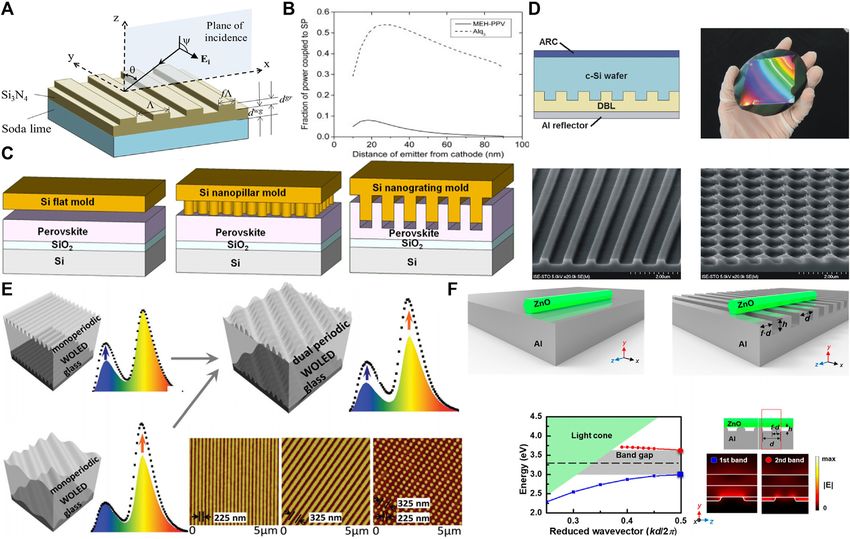
(Song et al., 2013; Yu et al., 2013; Yuan et al., 2018). In addition, excitation with the guided mode wavelengths (Collin, 2014). As
the microlens array can also enhance light trapping to improve shown in Figure 1A, Cunningham et al. fabricate Si3N4 periodic
the performance of optoelectronic devices (Choy et al., 2014; grating structures on a kind of soda-lime glass to form a GMR
Kang et al., 2015). More importantly, they can be used in 3D filter. While the GMR can be excited when the incident light
imaging systems with large view angles, high temporal resolution, satisfies Bragg diffraction by adjusting the period, depth of
and so on (Yuan et al., 2018). Except for the microlens array, grating, and thickness of waveguide (Liu et al., 2011; Ko and
Chueh et al. reported the pyramid-patterned sapphire substrate Magnusson, 2018). Rational grating structures can induce
could enhance the strong light interaction between MoS2 bilayers plasmonic effects because these structures can redistribute
and the substrate to improve photodetector performance (Wang optical fields and scatter light (Meinzer et al., 2014). Surface
et al., 2017). Moreover, it has been speculated that a perovskite plasmon polariton (SPP) loss usually appeared in OLED devices,
whispering gallery mode (WGM) microsphere array would have and the loss happened at the interface between dielectric and
higher optical absorption for solar cells (Grandidier et al., 2011; metal, which metal always serves as electrodes for OLED. And the
Mihi et al., 2013). And with the help of 3D structures of nanowire metallic film can couple light to induce SPP modes, which
and nanorod arrays, which make incident light undergo multiple transfer incident light into photo carriers (Atwater and
scattering inside the structure. They are usually used in various Polman, 2010). Actually, SPP is a guided electromagnetic
solar conversion devices to enhance light-harvesting ability (Cho surface mode with transverse magnetic polarization. In
et al., 2011). Nanorod array also can be applied in the field of general, the SPP modes coupled with excitons can’t support
light-emitting diodes (LED), Chang et al. reported a kind of LED the energy couple out from the OLED devices for the
that could adjust the polarization of the emitted light with the traditional planar OLED with non-grating structures. As
help of nanorod arrays (Chou et al., 2018). Every structure has shown in Figure 1B, Barnes et al. have illustrated that the SPP
unique properties, while the gratings architectures are more loss was up to ∼40% for traditional planar OLEDs, resulting in the
popular due to the simple fabrication process, easy adjusting obvious limitation on the OLED development (Hobson et al.,
of size and morph, and excellent performance of light trapping. 2002). It is noticed that the grating structures within OLED
The grating structure has been applied in most optoelectronic devices can realize light extraction effectively. Such as the
devices and other cutting-edge applications. It’s necessary to tunable grating array was fabricated on the metallic electrode
summarize the researches about grating structure in to match the SPP mode with the energy and momentum of light
optoelectronic devices. along with the interface, leading to the occurrence of SPP
In this minireview, we focus on the recent advancements in the resonance and increase of light extraction (Zayats et al., 2005).
application of grating structure in optoelectronic devices. Firstly, Besides the resonant effect and plasmonic effect, grating
the typical light trapping mechanisms of grating structures in structures also can improve light scattering efficiently due to
devices are discussed. And typical examples, such as the the structure prolong the optical path and increase the reflections
applications in photodetectors, solar cells, organic light- and refractions (Han and Chen, 2010; Chi et al., 2017). The
emitting devices, and lasers are summarized. Finally, the absorption ability always is limited by the Lambertian limit for
challenges and future perspectives for optoelectronic devices films. However, light scattering will be increased among the
with grating structures are also discussed. micro/nanostructures when the size of each structure is larger
than the wavelength. For example, the grating structures can
produce multiple reflections and refractions of the incident light,
MECHANISM leading to the prolongation of optical path length and the increase
of absorption to reach or exceed the Lambertian limit. There are
Micro/nanostructures largely determined the performance of two typical ways to fabricate the increased scattering surface,
optoelectronic devices due to they can influence the optical including integrating a textured layer and preparing ordered
properties of devices. However, it is important to balance the structures. Such as the grating structure with an appropriate
relationship between optical properties and electrical properties. periodicity that meets the condition of Bragg scattering can make
The light management mechanisms of grating structure in the light appear Bragg-scattered to enhance the light extraction
optoelectronic devices are usually summarized as the resonant (Bruetting et al., 2013; Cai and Qi, 2015).
effect, plasmonic effect and scattering enhancements. Among
various resonant strategies, the Mie theory is generally applied to
spherical structures and whispering gallery mode (WGM) usually THE APPLICATIONS IN OPTOELECTRONIC
used to the sphere, toroid, and ring structures. These structures DEVICES
can limit light circulate at the periphery of the resonator. As for
the grating structure, guided mode resonance (GMR) is applied. Photodetectors
The normally incident plane wave can be coupled into a The photodetector is a kind of typical optoelectronic device,
waveguide mode with the help of diffraction gratings (Yamada which can be adopted in many fields like clinical medical,
et al., 2017). The grating layer and supporting layer are necessary aerospace industry, military project, communication, and
for GMR. They can induce sharp reflection and transmission sensors since photodetector can convert the light signal into
anomalies. There will be a strong interaction between light and electrical signals for followed processes. However,
matter as long as it matches the outgoing emission or incoming photodetector development still faces low conversion
Frontiers in Chemistry | www.frontiersin.org 2 July 2021 | Volume 9 | Article 737679Wang et al. Grating Structures in Optoelectronic Devices FIGURE 1 | The grating structures in optoelectronic devices, (A) GMR filter with grating structure. (B) The calculated fraction of power lost from radiative excitons to surface plasmon modes is shown as a function of position of the exciton within the organic layer. (C). Schematic of nanoimprint lithography process with different Si molds. (D) The schematic diagram, photograph and SEM of the grating structures in solar cell. (E) Schematic of the broadband light extraction using OLED with dual- periodic grating structures and the morphologies of a serious of grating structures. (F) Schematic representation and characteristics of surface plasmon waveguide and periodic grating structures. Reproduced from Cunningham et al. (2011) with permission of Optical Society of America. Reproduced from Barnes et al. (2002) with permission of WILEY. Reproduced from Hu et al. (2016) with permission of American Chemical Society. Reproduced from Mellor et al. (2013) with permission of Optical Society of America. Reproduced from Sun et al. (2013) with permission of WILEY. Reproduced from Lin et al. (2018) with permission of American Chemical Society. efficiency, while the micro/nanostructures can improve the light Compared with flat perovskite photodetector, the detectivity and absorption by various strategies (Wang and Kim, 2017; Zhou and responsivity were improved by 7.8 and 6.7 times, respectively. In Huang, 2018). Among many structures, gratings play an essential practical applications, the polarization states of light usually have role. For example, Hu et al. reported an excellent perovskite more potential value. Hence, the detection of polarized light also is photodetector with nanograting through nanoimprint important. For example, Xia et al. reported a photodetector lithography (Figure 1C). The performance of photodetector was comprised of a stable 2D layered Ruddlesden–Popper perovskite improved after grating imprinted. The width of fabricated arranged in grating structures. And the photodetector performed nanograting was 270 nm, and the pitch was 600 nm, which high responsivity of 3.5 AW−1, detectivity exceeding 1 × 10¹⁵ Jones, could reduce reflectance during the entire spectrum. Meanwhile, and a fast response with a rise time of 4.1 ms and a decay time of the transmission also appeared to decrease in the range of 3.3 ms. It is noticed that the photodetector could realize 550–800 nm. In addition, perovskite film showed higher polarization detection, in which the photocurrent varies with crystallinity under the appearance of nanograting. The polarization angle due to the different dielectric constants of the combined effects lead to the improvement of ∼35 times in perovskite grating structures in different directions (Li et al., 2019). responsivity and ∼7 times in on/off current ratio (Wang et al., 2016). Besides the above traditional grating structure, more Solar Cells complex grating structures are applied in many devices The conversion of environmental energy into effective energy is gradually. Li et al. prepared a kind of moiré perovskite more critical for modern society. The solar cell is an effective photodetector using a stacked dual shallow grating structure strategy in this field. Solar cells usually absorb photons to induce (Song et al., 2021). The dual grating structure induced feedback the generation and transport of charge carriers, and the electric reflection, diffraction, and appearance of waveguide modes, energy was collected finally (Lewis, 2016; Polman et al., 2016). resulting in the enhanced light-harvesting of the photodetector. Although solar cells have been developed for many years, there Frontiers in Chemistry | www.frontiersin.org 3 July 2021 | Volume 9 | Article 737679
Wang et al.                                                                                               Grating Structures in Optoelectronic Devices

are still many problems, including the path length of light                applied in display and light panels with the advantages of
absorption mismatched the diffusion length of photo-                       color tunability, low cost, self-emitting property, and so on.
generated carriers. While the increase of path length of the               However, there is an obvious problem in organic light-
light absorption layer means the thickness of the absorbing                emitting devices, which is ∼80% generated photons are
layer increased, limiting the portability and the cost. The                trapped in devices leading to low light extraction efficiency. It
ordered grating structures can solve the above problems by                 is noticed that the ordered micro/nanostructures within the
unique optical properties without changing the thickness of                OLEDs can induce the outcoupling effect of trapped photons
light absorbing layer. Mellor et al. reported an excellent                 and regulate the emitting properties to improve light extraction
crystalline silicon solar cell with diffraction gratings fabricated        efficiency (Feng et al., 2017). During the internal light extraction
through nanoimprinted technology. As shown in Figure 1D, the               processes, about 40% SPPs mode loss happened around the
grating structure enhanced the incident light absorption                   interface between organic layer and electrode. And the grating
obviously, especially the crossed grating structure with the               structure can relieve SPP loss. Therefore, the fabrication of micro/
depth of 200 nm appeared the stronger ability in light                     nanostructures on a metal electrode is important because the
absorption than linear grating with the depth of 300 nm.                   electrode has better stability. Ma et al. prepared grating structures
Firstly, weakly absorbed photons were trapped and deflected                 on the ultrathin gold electrode through polymer-assisted thermal
into oblique orders through the diffraction gratings on the                nanoimprint technology, and the fabricated gratings were 320 nm
rear-side. Secondly, the path of light absorption was extended             in period and 60 nm in depth. Taking the advantages of
efficiently because the incident light was trapped within the               nanograting structures, the momenta of SPPs and photons
absorber layer by the total internal reflection of the front side           could realize momentum compensation to improve light
(Mellor et al., 2013). As mentioned above, the perovskite with             extraction and performance of OLEDs (Ma et al., 2020). For
grating structures can improve the ability of light absorption and         the white organic light-emitting devices (WOLEDs), broadband
scattering. At the same time, the crystallinity of perovskite also         light extraction is deserved to devote the effort. As shown in
was enhanced. Therefore, the patterned perovskite not only was             Figure 1E, Sun et al. reported a kind of WOLEDs involved dual-
applied in photodetector but also was applied in solar cells. Song         periodic gratings, in which the maximum current efficiency was
et al. reported a new imprinting method to fabricate the solar cells       enhanced by 37% (from 16.27 cd/A up to 22.33 cd/A). In
using the perovskite with grating structures as the active layer.          addition, compared to single periodic gratings, the dual-
And the larger area grating structures were fabricated by                  periodic gratings could broaden the SPP resonance (Bi et al.,
commercial optical discs, which the size of grating depended               2013). Besides the unpolarized light, the polarized light has
on the area of the CD or DVD (The diameter of CD and DVD is                become more and more important as an important and
12 cm). The improved scattering and absorption abilities of solar          appealing functional expansion in practical applications. And
cells can trap more incident light and suppress carrier                    the grating structures also was applied in OLEDs to emit linear
recombination simultaneously. Utilizing CD or DVD as a                     polarized light. Zhou et al. prepared a series of aluminum and
mold would have different grating structures, for example,                 polyurethane acrylate nanograting structures on the green OLED
when CD as a mold leading to the grating period and line                   substrate using developed soft nanoimprinting technology to
width was ∼1.5 and ∼1.0 µm, respectively. When DVD was a                   emit linear polarized light. The devices produced an angle-
mold, the grating period and line width was ∼0.75 and ∼0.5 µm,             invariant average extinction ratio as high as 20dB when the
respectively. And the heights of gratings were all ∼0.1 µm.                viewing angle within ± 60° due to both surface plasmons and
Actually, the height of structures will influence the                       cavity modes contributed to the TM-polarized light selection
performance of devices, such as the continuity of perovskite               (Zhou et al., 2020). At the same time, the development of
film can be broken when the height was exceeded the                         nanofabrication technology influences the light extraction
threshold value. On the opposite, the light trapping effect will           efficiency of OLEDs to a considerable degree. At present, there
be limited by the low height. Therefore, it is essential to consider       are two typical methods to fabricate grating structures, including
the range of height. Under the synergistic effect of the above             laser ablating method and nanoimprinting method. The laser
results, the power conversion efficiency and photocurrent density           ablation method takes advantages of simple processes and the
of perovskite solar cells with grating structures compared with            adjustable period according to the applied laser wavelength to
non-structures have been improved from 16.71 to 19.71% and                 reach the smaller grating period. However, the substrate may be
21.67 mA cm−2 to 23.11 mA cm−2. The authors have proved the                damaged by the high power of the laser during the ablation
grating structure has perfect homogeneity through the atomic               process. In contrast, the nanoimprint method can avoid the above
force microscope images. Additionally, the stability of perovskite         damages because nanoimprint is a secondary transfer process.
solar cells was also enhanced that the efficiency still keeps above         Therefore, compared to laser ablation, the nanoimprint method
90% after one month exposure on air (Wang et al., 2018).                   usually involves complex fabrication processes and the limitation
                                                                           of long periods. For example, Sun et al. utilized a simple one-step
                                                                           laser ablating method to prepare the OLEDs with periodic grating
ORGANIC LIGHT-EMITTING DEVICE                                              structures. The method of two interference beams was taken to
                                                                           avoid destroying the polymers because of the low ablation
Organic light-emitting devices (OLEDs) are a kind of essential             threshold. The grating structures play an important role in
and representative optoelectronic devices, which have been                 recovering power lost whatever in SPPs or waveguide mode,

Frontiers in Chemistry | www.frontiersin.org                           4                                        July 2021 | Volume 9 | Article 737679
Wang et al. Grating Structures in Optoelectronic Devices
and the efficiency was proved enhanced three times finally (Bai CONCLUSION AND OUTLOOK
et al., 2011).
In this minireview, we have summarized the mechanisms of
Lasers grating structures in photon-related devices, including
For the rapid development of integrated photonic circuits or chips, resonant effect, scattering enhancements, and plasmonic effect.
a miniature laser source is necessary. Laser with perfect intensity Taking advantages of light management strategies of grating
and directionality can be emitted from lasers through stimulated structures, the structures have been applied in many
emission of radiation and amplification. Organic-inorganic- optoelectronic devices, such as photodetectors, solar cells,
perovskites can be applied in miniature lasers due to their organic light-emitting devices, and lasers. Although the various
excellent and unique properties, including tunable bandgaps. For devices have proved the important role of grating structures
example, Gu et al. firstly reported perovskite distributed feedback successfully. However, there are still many bottlenecks that
resonator with grating structures using thermal nanoimprint need to be solved, including 1. how to improve the
lithography, which proposed a new method for the design and controllability of fabrication for grating structure; 2. how to
fabrication of perovskite lasers. The resonator performed the ability balance the relationship between optical and electrical
of narrow amplified spontaneous emission (The full width half- performance; 3. although the grating structure is more simple
maximum was 2.4 nm) even the pump power was only 0.1 W/cm2 than others, but decrease the cost and simplify the preparing
and a 16-fold reduction than pristine thin film (Gharajeh et al., processes are still crucial for applications in business.
2018). Actually, both light and electric sources can excite the lasers, Nevertheless, with the rapid developments of nanofabrication
such as Takenobu et al., who reported electroluminescence from a technologies, rational structure design, and advanced
single-crystal light-emitting transistor (LET) with a grating fundamental theories, more grating structures will be applied
resonator using the soft ultraviolet-nanoimprint lithography. in excellent optoelectronic devices, which will bring our better
And the electroluminescence could be controlled by the sub- daily life.
micrometer grating structure. Moreover, the final realization of
single-mode lasing depended on the Bragg diffraction and mode
coupling distributed feedback (DFB) system. The above research AUTHOR CONTRIBUTIONS
overcame the combination problem between LET and DFB
resonators (Maruyama et al., 2015). Except for frontier research, All authors listed have made a substantial, direct and intellectual
the lasers with grating structures have been applied in practical contribution to the work, and approved it for publication.
applications. Lin et al. reported a kind of hybrid plasmonic
nanolaser for sensing applications, and the role of Al grating
structures were plasmonic Bragg reflectors to decrease the FUNDING
mirror loss. As shown in Figure 1F, the nanolaser could serve
as a refractive index sensor to detect glucose solutions. The This work was supported by the National Natural Science
sensitivity of the nanolaser was 249 nm/RIU under the resonant Foundation of China (Grant No. 62004059, 62005074, and
wavelength of 373 nm (Cheng et al., 2018). Strong light trapping 61905062) and Natural Science Foundation of Hebei Province
ability will bring new paths for next-generation lasers. (No. F2021202047).
Chi, K., Yang, L., Liu, Z., Gao, P., Ye, J., and He, S. (2017). Large-scale
REFERENCES Nanostructured Low-Temperature Solar Selective Absorber. Opt. Lett. 42
(10), 1891–1894. doi:10.1364/OL.42.001891
Atwater, H. A., and Polman, A. (2010). Plasmonics for Improved Photovoltaic Cho, I. S., Chen, Z., Forman, A. J., Kim, D. R., Rao, P. M., Jaramillo, T. F., et al.
Devices. Nat. Mater 9 (3), 205–213. doi:10.1038/nmat2629 (2011). Branched TiO2Nanorods for Photoelectrochemical Hydrogen
Bai, Y., Feng, J., Liu, Y.-F., Song, J.-F., Simonen, J., Jin, Y., et al. (2011). Outcoupling Production. Nano Lett. 11 (11), 4978–4984. doi:10.1021/nl2029392
of Trapped Optical Modes in Organic Light-Emitting Devices with One-step Chou, M.-C., Lin, C.-Y., Lin, B.-L., Wang, C.-H., Chang, S.-H., Lai, W.-C., et al.
Fabricated Periodic Corrugation by Laser Ablation. Org. Electron. 12 (11), (2018). Polarization-Selecting III-Nitride Elliptical Nanorod Light-Emitting
1927–1935. doi:10.1016/j.orgel.2011.08.004 Diodes Fabricated with Nanospherical-Lens Lithography. ACS Nano 12 (8),
Bi, Y.-G., Feng, J., Li, Y.-F., Zhang, X.-L., Liu, Y.-F., Jin, Y., et al. (2013). Broadband 8748–8757. doi:10.1021/acsnano.8b04933
Light Extraction from White Organic Light-Emitting Devices by Employing Choy, W. C. H., Chan, W. K., and Yuan, Y. (2014). Recent Advances in Transition
Corrugated Metallic Electrodes with Dual Periodicity. Adv. Mater. 25 (48), Metal Complexes and Light-Management Engineering in Organic
6969–6974. doi:10.1002/adma.201302367 Optoelectronic Devices. Adv. Mater. 26 (31), 5368–5399. doi:10.1002/
Bruetting, W., Frischeisen, J., Schmidt, T. D., Scholz, B. J., and Mayr, C. (2013). adma.201306133
Device Efficiency of Organic Light-Emitting Diodes: Progress by Improved Collin, S. (2014). Nanostructure Arrays in Free-Space: Optical Properties and
Light Outcoupling. Phys. Status Solidi A App. Mater. Sci. 210 (1), 44–65. Applications. Rep. Prog. Phys. 77 (12), 126402. doi:10.1088/0034-4885/77/12/
doi:10.1002/pssa.201228320 126402
Cai, J., and Qi, L. (2015). Recent Advances in Antireflective Surfaces Based on Feng, J., Liu, Y.-F., Bi, Y.-G., and Sun, H.-B. (2017). Light Manipulation in Organic
Nanostructure Arrays. Mater. Horiz. 2 (1), 37–53. doi:10.1039/C4MH00140K Light-Emitting Devices by Integrating Micro/nano Patterns. Laser Photon. Rev.
Cheng, P.-J., Huang, Z.-T., Li, J.-H., Chou, B.-T., Chou, Y.-H., Lo, W.-C., et al. 11 (2), 1600145. doi:10.1002/lpor.201600145
(2018). High-Performance Plasmonic Nanolasers with a Nanotrench Defect Gao, X.-m., Liu, Y. F., Liu, Y.-f., Zhang, H.-j., Zhang, T.-r., Bi, Y.-g., et al. (2021).
Cavity for Sensing Applications. Acs Photon. 5 (7), 2638–2644. doi:10.1021/ Nanoimprinted Structures for Organic Light-Emitting Devices and Lasers.
acsphotonics.8b00337 Chin. J. Liq. Cryst. Disp. 36 (1), 8–20. doi:10.37188/cjlcd.2020-0277
Frontiers in Chemistry | www.frontiersin.org 5 July 2021 | Volume 9 | Article 737679Wang et al. Grating Structures in Optoelectronic Devices
Geng, C., Wei, T., Wang, X., Shen, D., Hao, Z., and Yan, Q. (2014). Enhancement of Improved Efficiency. ACS Nano 10 (12), 10921–10928. doi:10.1021/
Light Output Power from LEDs Based on Monolayer Colloidal Crystal. Small 10 acsnano.6b05535
(9), 1668–1686. doi:10.1002/smll.201303599 Wang, H., and Kim, D. H. (2017). Perovskite-based Photodetectors: Materials and
Gharajeh, A., Haroldson, R., Li, Z., Moon, J., Balachandran, B., Hu, W., et al. Devices. Chem. Soc. Rev. 46 (17), 5204–5236. doi:10.1039/C6CS00896H
(2018). Continuous-wave Operation in Directly Patterned Perovskite Wang, J.-N., Zhang, Y.-L., Liu, Y., Zheng, W., Lee, L. P., and Sun, H.-B. (2015).
Distributed Feedback Light Source at Room Temperature. Opt. Lett. 43 (3), Recent Developments in Superhydrophobic Graphene and Graphene-Related
611–614. doi:10.1364/ol.43.000611 Materials: from Preparation to Potential Applications. Nanoscale 7 (16),
Grandidier, J., Callahan, D. M., Munday, J. N., and Atwater, H. A. (2011). Light 7101–7114. doi:10.1039/C5NR00719D
Absorption Enhancement in Thin-Film Solar Cells Using Whispering Gallery Wang, S.-W., Medina, H., Hong, K.-B., Wu, C.-C., Qu, Y., Manikandan, A., et al.
Modes in Dielectric Nanospheres. Adv. Mater. 23 (10), 1272–1276. doi:10.1002/ (2017). Thermally Strained Band Gap Engineering of Transition-Metal
adma.201004393 Dichalcogenide Bilayers with Enhanced Light-Matter Interaction toward
Han, S. E., and Chen, G. (2010). Toward the Lambertian Limit of Light Trapping in Excellent Photodetectors. ACS Nano 11 (9), 8768–8776. doi:10.1021/
Thin Nanostructured Silicon Solar Cells. Nano Lett. 10 (11), 4692–4696. acsnano.7b02444
doi:10.1021/nl1029804 Wang, Y., Wang, P., Zhou, X., Li, C., Li, H., Hu, X., et al. (2018). Diffraction-Grated
Hobson, P. A., Wedge, S., Wasey, J. A. E., Sage, I., and Barnes, W. L. (2002). Surface Perovskite Induced Highly Efficient Solar Cells through Nanophotonic Light
Plasmon Mediated Emission from Organic Light-Emitting Diodes. Adv. Mater. Trapping. Adv. Energ. Mater. 8 (12), 1702960. doi:10.1002/aenm.201702960
14 (19), 1393–1396. doi:10.1002/1521-4095(20021002)14:193.0.Co;2-b Narrowband Filters Enabled by Guided-Mode Resonance in Two-Level
Kang, G., Yoo, J., Ahn, J., and Kim, K. (2015). Transparent Dielectric Waveguides. Opt. Lett. 42 (20), 4127–4130. doi:10.1364/OL.42.004127
Nanostructures for Efficient Light Management in Optoelectronic Yu, K., Fan, T., Lou, S., and Zhang, D. (2013). Biomimetic Optical Materials:
Applications. Nano Today 10 (1), 22–47. doi:10.1016/j.nantod.2015.01.008 Integration of Nature’s Design for Manipulation of Light. Prog. Mater. Sci. 58
Ko, Y. H., and Magnusson, R. (2018). Wideband Dielectric Metamaterial (6), 825–873. doi:10.1016/j.pmatsci.2013.03.003
Reflectors: Mie Scattering or Leaky Bloch Mode Resonance?. Optica 5 (3), Yuan, W., Li, L.-H., Lee, W.-B., and Chan, C.-Y. (2018). Fabrication of Microlens
289–294. doi:10.1364/OPTICA.5.000289 Array and its Application: A Review. Chin. J. Mech. Eng. 31 (1), 16. doi:10.1186/
Lewis, N. S. (2016). Research Opportunities to advance Solar Energy Utilization. s10033-018-0204-y
Science 351 (6271), aad1920. doi:10.1126/science.aad1920 Zayats, A. V., Smolyaninov, I. I., and Maradudin, A. A. (2005). Nano-optics of
Li, H., Gu, S., Zhang, Q., Song, E., Kuang, T., Chen, F., et al. (2021). Recent Surface Plasmon Polaritons. Phys. Rep. 408 (3), 131–314. doi:10.1016/
Advances in Biofluid Detection with Micro/nanostructured Bioelectronic j.physrep.2004.11.001
Devices. Nanoscale 13 (6), 3436–3453. doi:10.1039/d0nr07478k Zhang, Y.-L., Chen, Q.-D., Jin, Z., Kim, E., and Sun, H.-B. (2012a). Biomimetic
Li, S.-X., Zhang, G.-P., Xia, H., Xu, Y.-S., Lv, C., and Sun, H.-B. (2019). Template- Graphene Films and Their Properties. Nanoscale 4 (16), 4858–4869.
confined Growth of Ruddlesden-Popper Perovskite Micro-wire Arrays for doi:10.1039/C2NR30813D
Stable Polarized Photodetectors. Nanoscale 11 (39), 18272–18281. Zhang, Y.-L., Xia, H., Kim, E., and Sun, H.-B. (2012b). Recent Developments in
doi:10.1039/c9nr05396d Superhydrophobic Surfaces with Unique Structural and Functional Properties.
Liu, J.-N., Schulmerich, M. V., Bhargava, R., and Cunningham, B. T. (2011). Optimally Soft Matter 8 (44), 11217–11231. doi:10.1039/C2SM26517F
Designed Narrowband Guided-Mode Resonance Reflectance Filters for Mid-infrared Zhao, F., and Ma, D. (2017). Approaches to High Performance white Organic
Spectroscopy. Opt. Express 19 (24), 24182–24197. doi:10.1364/OE.19.024182 Light-Emitting Diodes for General Lighting. Mater. Chem. Front. 1 (10),
Ma, C., Liu, Y.-F., Gao, X.-M., Bi, Y.-G., Zhang, X.-L., Yin, D., et al. (2020). 1933–1950. doi:10.1039/C6QM00365F
Enhanced Efficiency of Organic Light-Emitting Devices by Using a Directly Zhmakin, A. I. (2011). Enhancement of Light Extraction from Light Emitting
Imprinted Nanopillared Ultrathin Metallic Electrode. Opt. Lett. 45 (17), Diodes. Phys. Rep. 498 (4), 189–241. doi:10.1016/j.physrep.2010.11.001
4879–4882. doi:10.1364/ol.402754 Zhou, J., and Huang, J. (2018). Photodetectors Based on Organic-Inorganic Hybrid
Maruyama, K., Sawabe, K., Sakanoue, T., Li, J., Takahashi, W., Hotta, S., et al. Lead Halide Perovskites. Adv. Sci. 5 (1), 1700256. doi:10.1002/advs.201700256
(2015). Ambipolar Light-Emitting Organic Single-crystal Transistors with a Zhou, L., Zhu, Y.-F., Zhang, Q.-Y., Zhou, Y., Wang, Y.-Z., Zhou, G.-H., et al.
Grating Resonator. Sci. Rep. 5. doi:10.1038/srep10221 (2020). Highly Linearly Polarized Light Emission from Flexible Organic Light-
Meinzer, N., Barnes, W. L., and Hooper, I. R. (2014). Plasmonic Meta-Atoms and Emitting Devices Capitalized on Integrated Ultrathin Metal-Dielectric
Metasurfaces. Nat. Photon 8 (12), 889–898. doi:10.1038/nphoton.2014.247 Nanograting. Opt. Express 28 (9), 13826–13836. doi:10.1364/oe.391624
Mellor, A., Hauser, H., Wellens, C., Benick, J., Eisenlohr, J., Peters, M., et al. (2013).
Nanoimprinted Diffraction Gratings for Crystalline Silicon Solar Cells: Conflict of Interest: The authors declare that the research was conducted in the
Implementation, Characterization and Simulation. Opt. Express 21 (5), absence of any commercial or financial relationships that could be construed as a
A295–A304. doi:10.1364/oe.21.00a295 potential conflict of interest.
Mihi, A., Bernechea, M., Kufer, D., and Konstantatos, G. (2013). Coupling Resonant
Modes of Embedded Dielectric Microspheres in Solution-Processed Solar Cells. Publisher’s Note: All claims expressed in this article are solely those of the authors
Adv. Opt. Mater. 1 (2), 139–143. doi:10.1002/adom.201200015 and do not necessarily represent those of their affiliated organizations, or those of
Polman, A., Knight, M., Garnett, E. C., Ehrler, B., and Sinke, W. C. (2016). the publisher, the editors and the reviewers. Any product that may be evaluated in
Photovoltaic Materials: Present Efficiencies and Future Challenges. Science 352 this article, or claim that may be made by its manufacturer, is not guaranteed or
(6283), aad4424. doi:10.1126/science.aad4424 endorsed by the publisher.
Song, Q., Wang, Y., Vogelbacher, F., Zhan, Y., Zhu, D., Lan, Y., et al. (2021). Moiré
Perovskite Photodetector toward High-Sensitive Digital Polarization Imaging. Copyright © 2021 Wang, Wang, Zhang, Sun, Yu and Lian. This is an open-access
Adv. Energ. Mater., 2100742. doi:10.1002/aenm.202100742 article distributed under the terms of the Creative Commons Attribution License (CC
Song, Y. M., Xie, Y., Malyarchuk, V., Xiao, J., Jung, I., Choi, K.-J., et al. (2013). BY). The use, distribution or reproduction in other forums is permitted, provided the
Digital Cameras with Designs Inspired by the Arthropod Eye. Nature 497 original author(s) and the copyright owner(s) are credited and that the original
(7447), 95–99. doi:10.1038/nature12083 publication in this journal is cited, in accordance with accepted academic practice.
Wang, H., Haroldson, R., Balachandran, B., Zakhidov, A., Sohal, S., Chan, J. Y., No use, distribution or reproduction is permitted which does not comply with
et al. (2016). Nanoimprinted Perovskite Nanograting Photodetector with these terms.
Frontiers in Chemistry | www.frontiersin.org 6 July 2021 | Volume 9 | Article 737679You can also read