Massachusetts Institute of Technology
←
→
Page content transcription
If your browser does not render page correctly, please read the page content below
Massachusetts Institute of Technology
Center for Space Research
Cambridge, MA 02139
Room 37-521
mwb@space.mit.edu
February 13, 2004
To: XIS Team
From: Mark Bautz, Steve Kissel, Beverly LaMarr & Gregory Prigozhin
Subject: Back-illuminated CCDs for Astro-E2 XIS?
1 Summary
This memo summarizes our recent work testing back-illuminated (BI) CCDs for possible use in the
XIS. We present measurements of quantum efficiency, spectral resolution, dark current & cosmetic
quality, proton radiation tolerance and background rejection efficiency for flight-like and flight-
candidate BI devices, and compare them to front-illuminated (FI) devices. Generally, we find that
the BI devices meet the expectations raised by the initial results we presented last November. In
particular, the BI devices offer quantum efficiency about 3× higher than the FI devices at 525
eV and spectral resolution comparable to that of the FI devices at all energies (BI FWHM within
∼ 15% of FI FWHM.) The BI devices have somewhat thinner depletion regions, leading to lower
quantum efficiency in the BI devices at high energies (e.g., by factors of ∼ 0.75 and ∼ 0.65 at
6.7 and 10 keV, respectively). The BI and FI devices have similar cosmetic quality. While the
BI devices show somewhat higher dark current than the FI devices, at the XIS CCD operating
temperature (-90C) the BI dark current has no effect on performance. The BI device appears to
be slightly more sensitive to proton radiation than the FI CCD, but the charge injection function
appears equally effective in suppressing radiation damage effects in the two kinds of sensor. The
background rejection efficiency of the BI devices is comparable to that of the FI devices at energies
below 1 keV, though, as on ACIS, the rejection efficiency is lower for the BI than the FI at higher
energies.
To date we have found no indication (after 400-500 total operating hours with 4 detectors, with
more than 24 thermal cycles on one detector) for any temporal instability in the BI device gain or
quantum efficiency. We have completed a calibration of one flight-candidate device at MIT, and
find that its quantum efficiency can be explained with a simple and physically reasonable model.
The optimum clock voltages for BI and FI devices differ, but both are well within the range
available from the XIS AE/TCE.
2 Overview
At the 2003 November XIS team meeting at ISAS, we reported that we had obtained promising
initial results with a back-illuminated version of the XIS (MIT/Lincoln Laboratory CCID41) CCD
detectors. The device we tested was produced using a so-called chemisorption backside treatment
process developed by M. Lesser at the Unviersity of Arizona [Lesser et al. 2004]. Since then we
have tested and/or calibrated four BI devices from two different wafers. We report our results here.
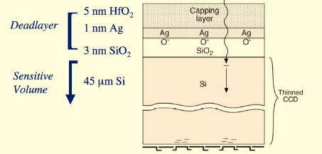
1Figure 1: Schematic of back-surface of a back-illuminated detector treated with the chemisorption
process. From Lesser et al., 2004.
In the next section we briefly describe the structure produced by the chemisorption backside
treatment process; subsequent sections describe quantum efficiency & spectral resolution, cosmetics,
dark current, radiation sensitivity and background rejection efficiency. The final sections summarize
our total test time with these detectors and outline differences in detector operating- and event
detection-parameters for FI and BI devices.
3 Backside structure produced by the chemisorption charging pro-
cess
The backside structure is shown schematically in Figure 1 from [Lesser et al. 2004]. The process
begins with a thinned wafer on which CCDs have already been fabricated. In our case, the wafers
are thinned, nominally, to 45µm. In the chemisorption charging process, the back surface of the
thinned wafer is first oxidized. The resulting 3 nm-thick oxide layer is then coated with a very thin
(∼ 1 nm) layer of silver; the silver is then capped with a 5nm layer of hafnium oxide. According
to [Lesser et al. 2004], the silver catlyzes dissociation of molecular oxygen on the surface during
processing, leaving fixed, negatively charged oxygen atoms on the surface. These ions improve the
collection of photo-electrons deposited near the back surface. Note that the gate structure of a
front-illuminated CCD presents a deadlayer ∼ 500 nm thick, so the chemisorption charging process
offers, in principle, a factor of ∼ 50 reduction in deadlayer thickness.
4 Measured Quantum Efficiency
Measured, spatially-averaged X-ray quantum detection efficiency (QE) for device w1.11c6 is shown
in Figure 2. The points were obtained using the standard CSR calibration procedure. The absolute
quantum efficiency was measured with respect to a (front-illuminated) reference CCD detector
that has been calibrated at the PTB beamline at the BESSY synchrotron. Random errors due to
counting statistics are neglible; systematic errors are probably about 5% of the measured quantum
2Material Thickness
Deadlayer Thicknesses:
SiO2 < 18 nm
HfO2 < 3 nm
Si 70 ± 23 nm
Sensitive layer thickness:
Si 37.6 ± 1.5µm
Table 1: Best-fit QE model parameter values for BI device w1.11c6. Upper limits and error ranges
are at 90% confidence for a single parameter.
efficiency at all energies above 277 eV. At 277 eV, the quantum efficiency of the reference detector
is not so well known, and we’ve assumed an error in the measured BI device QE of 25% in fitting
the model. For reference, typical FI device QE is shown as the dotted curve in Figure 2.
The BI quantum efficiency measurements shown in Figure 2 have not been corrected for pileup,
which may be significant at the lowest energies, so the actual QE of the device may be somewhat
higher than is shown in the figure at energies below 1 keV.
We fit deadlayer models containing the components shown in Figure 1, multiplied by an overall
scale factor and by an effective deadlayer of silicon to represent charge losses near the back surface.
We also allowed the overall thickness of the device (nominally 45µm) to be a free parameter in
the model. The best-fit model, shown as the solid line in Figure 2, has parameter values listed in
Table 1.
Three features of the best-fit model are particularly interesting. First, the very thin silicon
dioxide and hafnium oxide layers evidently have little effect on the device quantum efficiency; the
best-fit thicknesses for these layers are consistent with 0. Second, the model contains an apparent
deadlayer of silicon which, at ∼ 70nm is considerably thicker than the oxide layers, though much
thinner than the deadlayer of a front-illuminated CCD (∼ 550 nm). Finally, the apparent thickness
of the device is about 38 µm, which is less than the thickness of the depletion region in XIS front-
illuminated devices (60 − 65µm.) As a result, the quantum efficiency of the BI devices is less than
that of an FI device at energies E> 4.5 keV or so.
Finally, we compare the overall effective area of a single FI vs. a single BI XIS sensor in Figure 3.
Here we have included the XRT-I effective area and thermal shield (courtesy of Ishida-san) and
the XIS optical blocking filter (courtesy of Kitamoto-san.) This figure shows that the fractional
increases in effective area below 2 keV are generally much larger than the fractional loss of effective
area at high energies. Note that the BI CCD provides significant collecting area below the carbon
K-edge at 284 eV.
5 Spectral Resolution
The spectral resolution of BI and FI XIS devices is compared in Figure 4. The back-illuminated
CCDs we are considering for the XIS have spectral resolution quite comparable to that of FI
devices. In this regard they are quite different from all previous generations of back-illuminated
X-ray CCD devices, including those used on Chandra and XMM/Newton, which have spectral
resolution roughly a factor of two worse than similar FI devices.
Figure 4 shows that the XIS BI devices have spectral resolution that is comparable to, though
somewhat worse (FWHM ∼ 15 − 20% greater) than the FI devices at the lowest energies. The BI
3Figure 2: Measured absolute quantum efficiency (points) and best-fit quantum efficiency model
(solid line) for back-illuminated device w1.11c6. The best-fit measured QE of front-illuminated
XIS device w1.3c6 is shown as the dotted curve.
4Figure 3: Comparison of effective area, for one XIS sensor, for BI (red) and FI(black) CCDs. Note
that logarithmic axes are used. The XRT-I effective area, XRT thermal shield transmission, and
XIS optical blocking filter transmission are included in the calculation. The CCD efficiencies are
best-fit models to measurements of w1.11c6 (BI) and w1.3c6(FI), respectively.
5Figure 4: Comparison of spectral resolution (FWHM in eV) for back-illuminated (red points) and
front-illuminated (green points) XIS devices. The optimum split event thresholds are different for
the two device types. Data are from BI device w1.11c6 and FI device w1.7c5.
devices actually have slightly better spectral resolution at the highest energies. Note that, for the BI
devices, a split threshold of 7e− seems to provide the best compromise between quantum efficiency
and spectral resolution at low eneriges. (All BI quantum efficiencies reported were obtained with a
split threshold of 7e− ). The BI split threshold is thus considerably lower than the 13e− value used
for FI devices.
To compare the scientific quality of spectra produced by the two device types, we show in
Figure 5 simulated spectra for the supernova remnant E0102-72.3. In each case the count rates
pertain to a single XIS sensor. A very long exposure (105 s) to this bright source was simulated to
illustrate the response differences between the BI and FI devices. The spectral model is based on
the the Chandra HETG spectrum of this source ([Flanagan et al., 2004]). The simulations show
that the same spectral features are clearly resolvable by both devices, and that the BI devices
provide a factor of 3-4 higher counting rate at the O VIII Lyman α (0.66 keV) and OVII triplet
(0.57 keV), respectively. Integrated over the 0.2-2.5 keV band, the BI counting rate is a factor of
two greater than the FI counting rate for this source.
For comparison to current-generation CCDs, we compare in Figure 6 the simulated XIS spectra
of E0102-72.3 (repeated from Figure 5) to simulations (obtained with the same spectral model)
6Figure 5: Simulated spectra of the SNR E0102-72.3 for BI (red) and FI (green) devices. In each
case the counting rates are for a single sensor. The same spectral features are visible with both
device types but the BI device provides a counting rate higher by as much as a factor of 4 (at the
OVIII triplet at 0.57 keV.) The broadband (0.2-2.5 keV) couting rate is higher for the BI device
by a factor of 2.
of Chandra ACIS-S and XMM/Newton EPIC-PN observations of this source. The XIS BI device
provides much higher spectral resolution than either of the current generation observatories. Note
that a single XIS sensor is roughly equivalent in effective area in this energy range to Chandra
ACIS-S, while two XIS BI sensors provide about the same collecting area in as XMM-EPIC-PN,
but the XIS BI provides with much better spectral resolution than either ACIS or EPIC-PN.
6 Dark Current and Cosmetics
The mean (spatially averaged) dark current of BI and FI devices is shown as a function of tem-
perature in Figure 7. The BI devices have uniformly higher dark current. At a nominal operating
temperature of -90C, and a frame time of 8s, however, mean dark current will be less than 1 e−
pixel−1 per frame, and so is neglible from a performance point of view.
Statistics of hot pixels and bad columns are compared for a number of devices in Table 2. Hot
pixels have exceptionally high dark current, and are defined for purposes of this table as pixels
that show an anomalously high event rate (more than 10 standard deviations above the mean)
during X-ray calibration Although the total number of hot pixels seems to be higher in the BI
devices, most of these are concentrated in one or two defective columns. If these defective columns
are excluded, then the number of hot pixels is comparable in the BI and FI devices. It should be
noted that the effect of hot pixels depends on the method for dark level determination. The XIS
7Figure 6: Simulated spectra of the SNR E0102-72.38for XIS (top) ACIS-S (middle) and EPIC-PN (bottom) using a spectral model derived from Chandra grating data. The top panel shows both BI (red) and FI (green) spectra for one XIS sensor, repeated from the previous figure. One XIS BI sensor provides effective area equivalent to Chandra ACIS-S, and two are equivalent to XMM EPIC-PN in this energy range, but XIS BI has much better spectral resolution. (Vertical scales differ.)
Figure 7: Comparison of dark current measured for back-illuminated (red points) and front-
illuminated (green points) XIS devices. At the nominal frame time of 8s or less, and the nominal
operating temperature of -90C, dark current will be negligible for both device types.

                                               9
Device FI/BI Hot Pixels Bad Columns Remarks
Total Isolated
w1.14c8 FI 48 48 TBD Flight spare
w1.14c7 FI 18 18 34
w1.3c6 FI 54 30 27 24 hot pixels in worst column
w1.7c6 FI 45 45 36
w1.7c5 FI 31 31 24
w1.11c6 BI 635 39 TBD 596 hot pixels in 2 worst columns
w1.8c6 BI 1020 24 TBD 996 hot pixels in 2 worst columns
w1.8c5 BI 31 31 18 Flight candidate
Table 2: Hot pixel and defective column counts for the XIS flight FI devices and for several BI
devices. “Isolated” hot pixels are those remaining after one or two columns containing more than
10 hot pixels each are excluded.
DE provides for pixel-by-pixel dark level determination, so hot pixels can effectively be vetoed by
onboard processing.
A bad column is one in which at least 10% of the column is blocked and so effectively photo-
insensitive. Bad columns are identifed from very long (∼ 107 -event) exposures to an X-ray calibra-
tion source. The BI and FI devices have similar numbers of bad columns.
7 Radiation Tolerance
We have irradiated one front-illuminated and one back-illuminated XIS CCD with 40-MeV pro-
tons. The experiments were done at the Northeast Proton Therapy Center affiliated with the
Massachusetts General Hospital. In these tests, 235-MeV protons produced in a cylctron pass
through a plastic degrader, emerging with an energy of 40 MeV (± roughly 5 MeV). The proton
beam is then “collimated” by a ∼ 1 cm-diameter circular aperture in a ∼ 5 cm-thick lead shield
before striking the CCD. Thus only a portion of the (2.5 cm × 2.5 cm ) CCD is actually irradiated.
Devices are irradiated at room temperature with all leads shorted. For each device the total fluence
(2.0 ± 0.2 × 10⁹ protons cm−2 ) is delivered in a period of 1 minute or so. We esimtate that this
dose is equivalent to roughly 2 years exposure to on-orbit proton irradiation.
Protons of this energy increase dark current and charge transfer efficiency (CTI.) The change
in CTI manifests itself in decreasing pulse-height (“gain”) and declining spectral resolution with
increasing row number. Plots of the center-pixel pulse-height vs. row relationship both before and
after irradiation, for both BI and FI devices are shown in Figure 8. These curves were obtained
by illuminating the irradiated device with X-rays from a radioactive 55 Fe source; the detector
temperature was -90C during the CTI measurements. The slope of the pulse-height vs. row
characteritic is proportional to the CTI. The change in this slope, measured in the irradiated
portion of the CCD, gives the change in CTI due to the proton irradiation. Corresponding changes
in spectral resolution (FWHM at 5.9 keV) are shown in Figure 9.
The nominal CTI changes (at 5.9 keV) due to the proton irradiation are compared in Table 3.
The BI device appears to have experienced a somewhat larger change in CTI than the FI device,
by a factor of 1.5 ± 0.15. It is not clear why this is so. Three possibly contributing factors may
be i) The modest increase in linear energy transfer (dE/dx) of the incident protons as a result of
10Figure 8: Center-pixel pulseheight of 5.9 keV X-ray events vs CCD row number for BI (top) and
FI(bottom) devices irradiated with 2.0 ± 0.2 × 10⁹ p cm−2 of 40 MeV protons. Pre-irradiation data
are shown for comparison, and the effect of including charge-injection after the irradiated side is
also shown.
11Figure 9: Spectral resolution (FWHM)of 5.9 keV X-ray events vs CCD row number for BI (top)
and FI(bottom) devices irradiated with 2.0 ± 0.2 × 10⁹ p cm−2 of 40 MeV protons. Pre-irradiation
data are shown for comparison, and the effect of including charge-injection after the irradiation is
also shown.
12Device FI/BI CTI Change due to Irradiation
Without Charge Injection With Charge Injection
w1.8c6 BI 8.8 ± 0.7 1.6 ± 0.7
w1.6c1 FI 5.7 ± 0.2 0.4 ± 0.3
Table 3: Change in CTI (in units of 10−5 per pixel measured at 5.9 keV) due to irradiation by 40
MeV protons (nominal fluence 2.0 × 10⁹ protons cm−2 , roughly equivalent to 2 years of on-orbit
exposure) for the XIS BI and FI devices. Values obtained with and without charge injection are
listed.
traversing the ∼ 40µm thick silicon in the BI device before reaching the buried channel. This effect
might be expected to increase the BI radiation sensitivity we measure by about 10%, relative to
the FI devices; ii) the different clock voltages used for the two types of device; and iii) the smaller
sacrificial charge effect in the BI devices due to the absence of undepleted silicon. We note that
when charge injection is employed, the radiation sensitivity of both device types is significantly
reduced, and in fact is formally indistinguishable with these data.
8 Background Rejection Efficiency
In order to check the relative background rejection efficiencies of the FI and BI devices, one CCD
of each type was illuminated by a 60 Co source. The gammas and secondary electrons from this
source mimic, to some extent, the charged particle background encountered on-orbit. Standard
X-ray event selection criteria were applied, but for reasons described above in the discussion of
spectral resolution, the BI data were processed using a split-event threshold of 7 adu (roughly 1
adu ∼ 1 e− ) while a split threshold of 13 adu was used for the FI data. The resulting residual
background spectra are compared in Figure 10.
Figure 10 shows that, at energies below about 1.5 keV, the residual background (and hence the
charged particle background rejection efficiency) is about the same for the two detector types. In
the vicinity of the the silicon K fluorescence line at 1.74 keV, the BI rejection efficiency is much
better than the FI; integrated over the 1-2.5 keV, the BI rejection efficiency is better by a factor of
roughly 2. At higher energies, the FI rejection efficiency gets better relative to the BI. Integrated
over the 2.5 - 12 keV band, the FI rejection efficiency is better by a factor of about 2.5. The large
undepleted bulk of the FI devices evidently enhaces the the rejection efficiency for high-energy
particles, although it also apparently causes a brighter silicon fluorescence line.
9 Operating Experience
9.1 Test time summary
We have tested 4 BI devices to date, two each from two wafers. A third wafer is in process at this
writing. Wafer 11 devices were (intentionally) fabricated without charge injection. Wafer 8 devices
have charge injection.
We have subjected one device (w1.8c5) to a complete calibration (very roughly 200 hours of
operation over a three-week period. We believe this device is of flight quality and we expect to
install it in a flight sensor base during the month of February.
We have accumulated a total of approximately 300 hours of test time on the other three devices
over a four month period. One of these devices (w1.11c6) has received a nearly complete calibration
13Figure 10: Residual background spectra produced by a 60 Co source in BI (red) and FI (green)
CCDs. At energies below about 1.5 keV, the residual background (and hence the charged particle
background rejection efficiency) is about the same for the two detector types. At higher energies,
the FI rejection efficiency is better by a factor of about 3.
14and is not presently regarded as a flight candidate only beacuse it is not equipped with charge
injection. Another device (w1.8c6) has been subjected to at least 24 thermal cycles; this same
device has been irradiated with 40 MeV protons. Once the proper operating point for the BI
devices was established (see below), we found no evidence for peculiar or unstable behavior. We
are continuing testing to check stability.
We expect delivery of additional BI devices (from the third wafer to be treated with the
chemisorption charging process) within the month.
9.2 Differences between FI and BI device operating points.
Currently the FI uses +7 -6 volt serial clocks (dacs=140, 120). These values have propagated from
the original Astro-E design. While there is some evidence that they may not be optimal these
values provide good performance in the FI devices. For the (4) BI devices we have found that these
levels are inappropriate since they produce noise in excess of 20e per readout. Instead, values of
+4.5 -4.5 volt (dacs=90, 90) are used for the serial clocks. Further reduction of serial clock level
complicates the charge injection operation and does not improve performance.
The current BI devices do not work well if the image clock level moves into inversion. For
this reason we use +12 -2.5 volts for the image clock and for convenience have removed the SEQI
commands from the sequencer. The SEQI commands could be restored if power consumption
during parallel transfer becomes an issue. A consequence of these image clock voltages is that a
one-time “jitter dacs” step is required each time the CCD is power is turned on . (Such a step is
routinely used in ACIS operations.) As expected, the BI produces more split events at all energies
than does the FI. Consequently the importance of the previous noise-reduction steps is magnified
since more pixels are used per event. Also, the split threshold for the BI needs to be lower to
recover event charge.
References
[Lesser et al. 2004] Burke, B., Lesser, M. et al. 2004 IEEE Nuclear Science Symposium (submitted).
[Flanagan et al., 2004] Flanagan, K.A., Canizares, C. R., Dewey, D., Houck, J. C., Fredericks, A.
C., Schattenburg, M. L., Markert, T. H. & Davis, D. S., 2004, ApJ, (in press). (astro-ph/0312509)
15You can also read