Reliable Nanofabrication of Single-Crystal Diamond Photonic Nanostructures for Nanoscale Sensing
←
→
Page content transcription
If your browser does not render page correctly, please read the page content below
micromachines

Article
Reliable Nanofabrication of Single-Crystal Diamond
Photonic Nanostructures for Nanoscale Sensing
Mariusz Radtke † , Richard Nelz              , Abdallah Slablab   and Elke Neu *
 Faculty of Natural Sciences and Technology, Saarland University, Physics, Campus E2.6,
 66123 Saarbrücken, Germany
 * Correspondence: elkeneu@physik.uni-saarland.de
 † Current address: Department of Organic and Macromolecular Chemistry, Ghent University Krijgslaan 281,
   building S4, 9000 Gent, Belgium.

 Received: 26 September 2019; Accepted: 17 October 2019; Published: 24 October 2019

 Abstract: In this manuscript, we outline a reliable procedure to manufacture photonic nanostructures
 from single-crystal diamond (SCD). Photonic nanostructures, in our case SCD nanopillars on thin
 (
Micromachines 2019, 10, 718                                                                         2 of 10

magnitude slower than SCD using typical etching recipes [12]. In general, HSQ enables creating
very small mask structures down to 20 nm [13]. SCD structures etched using HSQ masks show
smooth sidewalls [12]. Smooth sidewalls ensure low light scattering from photonic structures and
defined waveguide properties. Consequently, HSQ masks enable etching almost cylindrical pillars with
optimized shape and well-defined photonic properties [6,9,12,14,15]. On the other hand, we find that
HSQ has a non-optimal adhesion to SCD. In previous work, this challenge has often been addressed
using metallic inter-layers between HSQ and SCD, e.g., titanium [16]. However, even very thin
(
Micromachines 2019, 10, 718 3 of 10
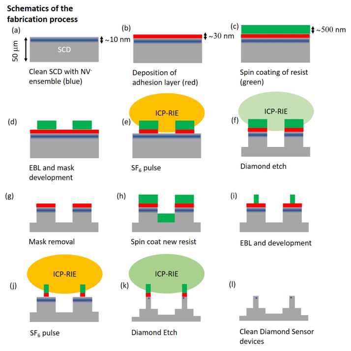
Figure 1. (a) The process starts with an SCD sample with a shallow layer of NV centers. Subsequently,
we deposit (b) a silicon adhesion layer and (c) spin coat HSQ. (d) We use electron beam lithography
(EBL) to structure the HSQ resist and obtain masks for the platforms. Using ICP-RIE, (e) we remove
the silicon layer in-between the HSQ mask and (f) perform the structuring etch for SCD. (g) We finalize
platform structuring via removing residual HSQ. We now (h) spin coat HSQ onto the remaining silicon
layer and (i) perform EBL again. We repeat the ICP-RIE procedure, firstly (j) removing the silicon layer
and then (k) etching the pillars into SCD. In a last step, (l) we remove residual HSQ as well as silicon to
obtain clean SCD devices.
2. Sample Pre-Treatment
We purchased high-purity, (100)-oriented, chemical vapor deposited, SCD from Element Six
(electronic grade quality, [N]s < 5 ppb, B < 1 ppb). As we aimed for free standing SCD devices
consisting of nanopillars on platforms, the SCD plates (size 2 × 4 mm2 ) were polished down to
thickness of 50 µm (Delaware Diamond Knives, Wilmington, DE, US). The SCD surface showed an
initial roughness of Ra < 3 nm. As the mechanical polishing of the SCD can leave highly contaminated
surfaces, we first wiped the sample surface using clean-room wipes and performed cleaning in an
ultrasonic bath (solvents: isopropanol and acetone). We then cleaned the sample in boiling acids
(1:1:1 mixture of sulfuric acid, perchloric acid and nitric acid, 5 mL each).
Mechanical polishing is suspected to introduce damage that potentially extends several
micrometers deep into the SCD material [19,20]. To remove this potentially damaged and strained
material, we applied ICP-RIE to our SCD samples. We avoided the use of toxic or corrosive gases in
the process following our previously published routine [21]. We used a Plasmalab 100 ICP-RIE reactor
(Oxford instruments, Abington, UK) and removed the topmost 3–5 µm of SCD from each side. WeMicromachines 2019, 10, 718 4 of 10
used a combination of SF6 ,O2 , Ar biased plasmas with mixed RF and ICP discharges. Following recent
approaches [22,23], we terminated the etching using low-damage, 0 V bias plasma with pure oxygen.
The use of such soft etching was motivated by the potential close-to-surface damage due to highly
biased ICP etching [24]. We typically obtain very smooth surfaces with an rms roughness of ∼1 nm.
Using the above described procedure, we avoided creating NV centers in potentially damaged
SCD. We formed a homogeneous layer of NV− centers by implanting nitrogen ions with a density of
2 × 10¹¹ ions/cm2 and an energy of 6 keV. During the implantation, the sample was tilted by 7◦ with
respect to the ion beam to avoid ion channeling. The SCD sample was then annealed in vacuum at
800 ◦ C followed by an acid clean. This treatment will typically leave our sample with a mixed oxygen
termination on the surface [25]. We found a contact angle for water of 67◦ [26], indicating a hydrophilic
surface. As the electron beam resist we want to apply to the SCD was dissolved in methyl isobutyl
ketone, a polar molecule, the resist’s solvent had high affinity to hydrophilic surfaces. Despite the,
in principle, fitting surface termination of the SCD sample, we observed non-reliable adhesion when
applying HSQ to the SCD surface.
3. Deposition of Adhesion Layer and HSQ Mask Structuring
Motivated by the lack of reliable adhesion of HSQ to clean SCD surfaces, we explored silicon as
an inter-layer. We expect this layer to foster adhesion between polysilicate HSQ resist and the native
oxide (SiO2 ) on the layer. To deposit the silicon adhesion layer, we used electron beam evaporation at
a pressure of 10−6 Torr and 10 kV acceleration voltage with elliptical beam scanning mode in an electron
beam evaporator “Pfeiffer Classic 500 L” machine. For the present work, we chose a thickness of the
silicon layer of 25 nm. We note that we also found sputtered silicon layers to efficiently foster adhesion
between SCD and HSQ. However, the SCD surface was attacked during the sputtering process. This in
our case led to excess blinking and bleaching of NV− centers in the final sensing devices and rules out
this approach for our application. We also note that we tested spin coating Ti-prime as an adhesion
promoter but did not obtain reliable results. We furthermore tested chromium layers as alternative
to quickly oxidizing titanium layers [16]. Using this approach, we faced micromasking effects most
probably arising from the incomplete, non-reliable wet-chemical removal of chromium layers. We note
that our silicon layers still enable efficient HSQ adhesion weeks after deposition and storage under
ambient conditions. We consequently conclude that the formation of a native oxide layer on the silicon,
which will occur during storage at ambient conditions, is not detrimental. Thus, technically speaking,
evaporation of silicon layers can be performed in batch processes for several SCD samples, which
eases the fabrication workflow and reduces machine time. The evaporated silicon layers are very
uniform and show a low roughness, as evidenced by AFM. We note that adhesion of the silicon layer to
SCD was very reliable and we never observed any hints of cracking or peeling throughout the whole
process, deduced from AFM and SEM microscopy. We have processed more than 10 samples using the
here described method and no SEM images showed peeling or cracking of the silicon layer. To avoid
any damage of the surface caused by contact with the tip (AFM) or amorphous carbon deposition
(from SEM chamber), no routine checks were performed prior each fabrication step. We note we also
observed the surface topography of samples covered with HSQ layers. In case of any silicon peeling,
this would be evident by folding of spin-coated HSQ.
To manufacture etch masks based on HSQ, we used Fox 16 resist (Dow Corning, Midland, MI,
USA), which we spin-coated onto the SCD plate. To ease handling of our small SCD plates, we glued
them to silicon carrier chips using crystalbond adhesive. We note that the silicon carrier can be removed
at the end of our nanofabrication process using acetone to dissolve crystalbond without damage to the
SCD nanostructures. Prior to spin coating, we heated the SCD sample on the silicon carrier for 10 min
at 120 ◦ C to remove any moisture from the surface. We applied roughly 0.3 mL of Fox 16 solution
to the SCD plate and spin-coated it at 1000 rpm for 10 s then increasing rotation speed to 3300 rpm
for 60 s. Subsequently, we pre-baked the sample at 90 ◦ C for 5 min. We note that great care has been
taken to not exceed the shelf life of the Fox 16 resist. As a result of the small size of our samples asMicromachines 2019, 10, 718 5 of 10
well as the spin coating on already etched structures in the latter stages of our fabrication process,
we can only estimate the thickness of the HSQ, which shows a significant variation from sample to
sample. From SEM images of pillar masks on platforms, we estimate a HSQ layer thickness of ∼0.9 µm.
Consequently, considering a pillar diameter of ∼200 nm, we demonstrate reliable adhesion of HSQ
masks with an aspect ratio of 4.5.
We inserted the SCD plate including the silicon carrier chip into our EBL machine (cold-cathode
SEM, Hitachi S45000, Chiyoda, Japan, equipped with RAITH Elphy software). We note that EBL of the
spin-coated HSQ layer has to be done directly after spin coating to avoid any reaction of HSQ with air.
We performed EBL at 30 kV acceleration voltage and 20 µA extracting current. The working distance is
kept at 15.3 mm for 400 × 400 µm2 fields. During our device fabrication, larger structures, namely the
rectangular holding platforms (size ∼ 3 × 20 µm2 ) as well as masks for nanopillars (diameter 200 nm),
were of interest. We wrote platforms using longitudinal writing mode and pillars using concentric
writing modes. The doses for large structures were established to be optimal as 0.49 mC/cm2 and
for pillar structures, with a variation with thickness of the HSQ layer, between 2.24 (planar SCD) and
7 mC/cm2 (pre-structured SCD with, e.g., platforms).
We developed the HSQ in 25% TMAH solution without swirling the solution. After 20 s, the SCD
sample was placed in ultra-pure 18 MOhm cm MiliQ water and subsequently immersed several times
in acetone and isopropanol. We note that the development has to take place directly after removing
the SCD plate from the EBL vacuum chamber.
4. Selective ICP-RIE of Adhesion Layer and SCD Structuring
A dedicated ICP/RIE plasma sequence based on O2 -based etching of SCD, preceded by a short
pulse of SF6 plasma, was designed. This sequence first selectively removes the silicon layer
between the HSQ-based mask structures and subsequently enables highly anisotropic etching of
SCD. The parameters of the plasmas are summarized in Table 1. In the final process, we ran the above
mentioned sequence without removing the sample from the ICP-RIE reactor in-between the plasma
steps to avoid any contamination.
Reliably removing the silicon layer without any residuals is vital to our process: We observed
a partial etch stop as well as strong micromasking when applying the O2 -based plasma without
applying the SF6 pulse (see Figure 2a). We deduced a complete and reliable removal of the silicon
adhesion layer from two facts: First, in SEM images taken directly after the SF6 pulse (see Figure 2b),
a clear contrast between etched and non-etched areas is visible. We also investigated the SF6 -based
etching process by means of optical emission spectroscopy shown in Figure 2c. In the spectrum a series
of emission lines corresponding to fluoride (F− ) was observed [27]. We attributed the etching of silicon
to this F− ions. Second, knowing that the O2 plasma used to etch SCD was not etching the silicon layer,
the absence of micromasking and very smooth surfaces in-between the etched structures (see Figure 3a)
proved the complete removal of the silicon layer. We note that using pure SF6 is vital to arrive at this
result, as introduction of other gases (Argon or Oxygen) at this stage generated severe micromasking.
Our SF6 plasma removes the silicon layer while maintaining a 1:20 selectivity in favor of the HSQ
mask. For our process, this means that, during removal of the 25 nm thick silicon adhesion layer, less
than 2 nm of the HSQ mask, which in our case is several hundreds of nanometer thick, will be lost.
This result corresponds well to similar plasmas obtained in different systems showing highly selective
silicon etching while conserving SiO2 (in our case HSQ) [28]. We furthermore observed no or minor
etching of SCD during the SF6 pulse and no roughening of the exposed SCD surface. We confirmed
full etching of the silicon layer using Raman spectroscopy and XPS, whereas the latter only showed
C1s and O1s peaks. Using EDX, we checked that there is no silicon contamination on the etched SCD
after the O2 -based plasma (see Figure 4).Micromachines 2019, 10, 718 6 of 10
Table 1. Etching plasma parameters. SF6 pulse used to selectively remove the evaporated silicon layer
(5 s including plasma ignition step). The O2 plasma is subsequently used as an anisotropic etch for
SCD to form the platforms as well as the pillars (10–15 min etching time).
Plasma ICP Power RF Power Gas Flux Etch Rate Pressure
W W sccm nm/min Pa
SF6 pulse 300 100 SF6 :25 Si: 1072 HSQ: 52 1.3
O2 plasma 500 200 O2 : 50 104 1.5
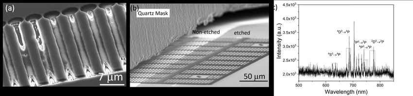
Figure 2. (a) Pattern of holding platforms etched with O2 plasma without applying the SF6 pulse plasma
to remove the silicon layer, the SEM image shows the bare SCD structures. Strong micro-masking and
corresponding roughening as well as a partial etch stop are visible (b) Scanning electron microscope
(SEM) image of SCD surface with HSQ structures, here platforms, after SF6 pulse. A part of the
platforms is covered with a quartz plate (marked in the image) during the SF6 pulse. The strongly
reduced brightness of the etched surface in contrast to non-etched surface indicates the complete
removal of the silicon adhesion layer. We furthermore observe no or minor etching of SCD during
the SF6 pulse and no roughening of the exposed SCD surface. (c) Optical emission spectrum of the
SF6 pulse plasma step indicating presence of fluoride (F− ) species responsible for selective removal of
silicon from the SCD surface.
Figure 3. (a) Devices at intermediate stage of the process with etched-in platforms. Note that the SEM
image shows the bare SCD structures that have been obtained via removing the adhesion layer using
the SF6 pulse followed by anisotropic O2 RIE and subsequent cleaning. (b) HSQ masks for pillars
etching written by EBL. The masks are residing on SCD platforms coated by a freshly evaporated
silicon layer. Note that the silicon layer is not discernible in the SEM images.
After successfully structuring our SCD platforms, we removed HSQ residuals using HF-based
buffered oxide etch by immersion of SCD for 20 min in the solution. Although this step removed the
native oxide from our silicon adhesion layer, the layer itself survived the process, as clearly discernible
from the EDX imaging in Figure 4b. Consequently, it can be re-used for consecutive steps. We then
spin-coated HSQ again, which in our case formed a layer on top as well as in-between the platforms.
We then re-emploedy EBL to create pillar masks on the platforms (see Figure 3b). We repeated the
etching to transfer the pillar mask into the SCD platform creating almost cylindrical pillars.Micromachines 2019, 10, 718 7 of 10
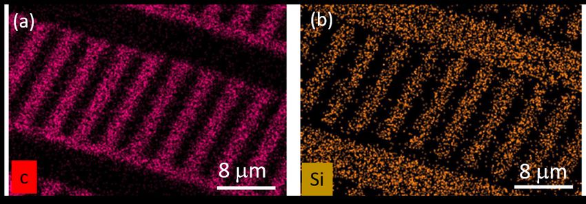
Figure 4. Energy dispersive X-ray (EDX) spectroscopy mapping of SCD cantilevers prepared by the
presented method. The EDX mapping has been performed after the SF6 plasma, the O2 plasma etching
the SCD structures (parameters see Table 1) and the wet chemical removal of residual HSQ: (a) carbon
signal; and (b) silicon signal. The two maps show complementary images, clearly indicating that,
in-between the platforms, we find bare SCD (carbon) with no silicon signal while on the platform,
the silicon adhesion layer survived and is ready to be used in the next processing step.
5. Final Devices and Device Characterization
To obtain clean SCD devices, we removed all HSQ residuals using HF-based buffered oxide
etch. We immersed the SCD into buffered oxide etch for 20 min which removes the HSQ as well as
any native oxide on the silicon layer. Afterwards, we immersed the SCD sample in 3M potassium
hydroxide at 80 ◦ C for 30 min to remove the silicon adhesion layer and revealed the clean SCD
structures. After this process, we repeated the three-acid cleaning described above before characterizing
the photoluminescence (PL) of NV− centers in the SCD nanostructures. Figure 5a displays devices
obtained using this process. We note that, to obtain free standing devices, which we mounted to quartz
capillaries as holders (see Figure 5b), the SCD plate has to be thinned from the non-structured side
until the devices are fully released. For more details on the mounting, see Reference [16]. To this
end, we employed previously published deep-etching routines [21] which are beyond the scope of
this manuscript.
Figure 5. Scanning probe devices manufactured using the described nanofabrication process. (a) Pillars
on platforms. The shown devices still need thinning of the SCD plate from the backside to release the
devices. (b) Mounted SCD scanning probe. On the right hand side, a quartz capillary is visible that
serves as a holder to mount the device to a scanning probe microscope.
To investigate the photonic properties of our SCD nanostructures, we used a custom-built confocal
microscope (numerical aperture 0.8). Details of the setup are given in References [22,29–31].
We first measured confocal PL maps of the structures (see Figure 6a,b) excited at 532 nm with
a power of 500 µW. We clearly observed intense PL (∼100 kcps) originating from single NV− centers
in the pillars (see Figure 6a). We estimated the maximum achievable PL of the NV− centers to be
>300 kcps comparable to previous work [16]. In addition, we investigated the background PL from
the etched surface (∼1 kcps), which is negligible compared to the NV− center PL from the pillar
(see Figure 6b).Micromachines 2019, 10, 718 8 of 10
Keeping background PL from etched surfaces low is important as it limits the signal-to-
background ratio and consequently the achievable magnetic field sensitivity [32]. Figure 6c shows an
exemplary optically detected magnetic resonance (ODMR) measured on single NV− centers in the
structures. Here, we measured an ODMR contrast of ∼15%. By investigating the coherence of the
NV− centers in the nanostructures, we found a coherence time of T2 ≤10 µs. We attributed this to the
NV− centers’ proximity to the surface which is in a good agreement with results from other groups
measuring the coherence of shallow NV− centers in three-acid-cleaned SCD [33]. Considering the
already low T2 , we cannot fully exclude a negative influence of the structuring on T2 .
(a) (b) (c)
Figure 6. (a,b) PL map of SCD platforms with individual nanopillars fabricated with the process
described in Section 4. The outer edge of the holding platform is indicated using a dashed line,
while the pillars appear as bright spots. To enable comparing the background PL from the platforms
with the PL of a few NV− centers in the pillars, we show the same PL map with two different scaling:
individual NV− centers in the pillars show PL countrates above 125 kcps at an excitation power
of 500 µW at 532 nm (a). (b) It is clearly discernible that the cantilevers show only a weak PL of
∼ 1 kcps. The enhanced background in-between the platform arises from a slight roughening between
the structures. We detect NV− PL in the wavelength range >650 nm. (c) An exemplary optically
detected magnetic resonance (ODMR) of one of the NV− centers in the pillar. The resonance (without
an external magnetic field) at 2.87 GHz is clearly visible and has a contrast of ∼15%.
6. Summary and Conclusions
In this paper, we present a reliable technology for nanofabrication of SCD structures. We used our
method to manufacture SCD scanning probes with shallowly embedded negative nitrogen vacancies.
The method introduces an evaporated silicon adhesion layer on the SCD surface to ease adhesion and
EBL with spin-coated HSQ-based Fox 16 resist. We present a methodology for the selective removal
of our silicon adhesive/decharging layer with SF6 plasma. In areas protected by the HSQ mask,
silicon layer survives etching as well as wet chemical removal of the residual HSQ mask and can be
re-used for further nanofabrication, in our case for pillars on SCD platform. The shallowly implanted
NV− centers survived the nanofabrication process. We found this method to be reliable, which is
a considerable advancement in SCD nanofabrication technology that can be expanded to various kinds
of SCD structures including SCD cantilever or cavity structures (e.g., photonic crystals).
Author Contributions: Funding acquisition, E.N.; Investigation, M.R., R.N., A.S. and E.N.; Methodology, M.R.,
R.N., A.S. and E.N; Supervision, E.N.; Writing—original draft, M.R., R.N. and E.N.; Writing—review and editing,
M.R., R.N., A.S. and E.N.
Funding: This research was funded by NanoMatFutur grant of the German Ministry of Education and Research
(FKZ13N13547).
Acknowledgments: We would like to acknowledge Sandra Wolff (TU Kaiserslautern, Germany) for help with
electron beam evaporation, Jörg Schmauch (INM, Germany) for his help with acquiring high-quality SEM images
and Rene Hensel (INM, Germany) for granting access to the ICP/RIE reactor. We acknowledge Michel Challier for
his assistance and Andreas Ruh (Saarland University, Germany) for his help with EDX. We gratefully acknowledge
cooperation and fruitful discussion with QNAMI (Basel), especially with Felipe Favaro De Oliveira and Patrick
Maletinsky on the evaluation of our novel nanofab method. We note that the results presented in this study are
filed for a patent, application number: EP19198772.6.Micromachines 2019, 10, 718 9 of 10
Conflicts of Interest: The authors declare no conflict of interest.
References
1. Atatüre, M.; Englund, D.; Vamivakas, N.; Lee, S.Y.; Wrachtrup, J. Material platforms for spin-based photonic
quantum technologies. Nat. Rev. Mater. 2018, 3, 38. [CrossRef]
2. Casola, F.; van der Sar, T.; Yacoby, A. Probing condensed matter physics with magnetometry based on
nitrogen-vacancy centres in diamond. Nat. Rev. Mater. 2018, 3, 17088. [CrossRef]
3. Kucsko, G.; Maurer, P.; Yao, N.; Kubo, M.; Noh, H.; Lo, P.; Park, H.; Lukin, M. Nanometre-scale thermometry
in a living cell. Nature 2013, 500, 54–58. [CrossRef] [PubMed]
4. Teissier, J.; Barfuss, A.; Appel, P.; Neu, E.; Maletinsky, P. Strain coupling of a nitrogen-vacancy center spin to
a diamond mechanical oscillator. Phys. Rev. Lett. 2014, 113, 020503. [CrossRef] [PubMed]
5. Dolde, F.; Doherty, M.W.; Michl, J.; Jakobi, I.; Naydenov, B.; Pezzagna, S.; Meijer, J.; Neumann, P.; Jelezko, F.;
Manson, N.B.; et al. Nanoscale detection of a single fundamental charge in ambient conditions using the
NV- center in diamond. Phys. Rev. Lett. 2014, 112, 097603. [CrossRef] [PubMed]
6. Maletinsky, P.; Hong, S.; Grinolds, M.; Hausmann, B.; Lukin, M.; Walsworth, R.; Loncar, M.;
Yacoby, A. A robust scanning diamond sensor for nanoscale imaging with single nitrogen-vacancy centres.
Nat. Nanotechnol. 2012, 7, 320–324. [CrossRef] [PubMed]
7. Neumann, P.; Kolesov, R.; Naydenov, B.; Beck, J.; Rempp, F.; Steiner, M.; Jacques, V.; Balasubramanian, G.;
Markham, M.L.; Twitchen, D.J.; et al. Quantum register based on coupled electron spins in
a room-temperature solid. Nat. Phys. 2010, 6, 249–253. [CrossRef]
8. Kurtsiefer, C.; Mayer, S.; Zarda, P.; Weinfurter, H. Stable solid-state source of single photons. Phys. Rev. Lett.
2000, 85, 290–293. [CrossRef]
9. Babinec, T.; Hausmann, B.; Khan, M.; Zhang, Y.; Maze, J.; Hemmer, P.; Loncar, M. A diamond nanowire
single-photon source. Nat. Nanotechnol. 2010, 5, 195–199. [CrossRef]
10. Gruber, A.; Dräbenstedt, A.; Tietz, C.; Fleury, L.; Wrachtrup, J.; von Borczyskowski, C. Scanning confocal
optical microscopy and magnetic resonance on single defect centers. Science 1997, 276, 2012–2014. [CrossRef]
11. Zaitsev, A. Optical Properties of Diamond: A Data Handbook; Springer: Berlin, Germany, 2001.
12. Hausmann, B.J.; Khan, M.; Zhang, Y.; Babinec, T.M.; Martinick, K.; McCutcheon, M.; Hemmer, P.R.; Loncar, M.
Fabrication of diamond nanowires for quantum information processing applications. Diam. Relat. Mater.
2010, 19, 621–629. [CrossRef]
13. Grigorescu, A.; Hagen, C. Resists for sub-20-nm electron beam lithography with a focus on HSQ: State of
the art. Nanotechnology 2009, 20, 292001. [CrossRef] [PubMed]
14. Neu, E.; Appel, P.; Ganzhorn, M.; Miguel-Sanchez, J.; Lesik, M.; Mille, V.; Jacques, V.; Tallaire, A.; Achard,
J.; Maletinsky, P. Photonic nano-structures on (111)-oriented diamond. Appl. Phys. Lett. 2014, 104, 153108.
[CrossRef]
15. Fuchs, P.; Challier, M.; Neu, E. Optimized single-crystal diamond scanning probes for high sensitivity
magnetometry. New J. Phys. 2018, 20, 125001. [CrossRef]
16. Appel, P.; Neu, E.; Ganzhorn, M.; Barfuss, A.; Batzer, M.; Gratz, M.; Tschöpe, A.; Maletinsky, P. Fabrication
of all diamond scanning probes for nanoscale magnetometry. Rev. Sci. Instrum. 2016, 87, 063703. [CrossRef]
17. Lillie, S.E.; Broadway, D.A.; Dontschuk, N.; Zavabeti, A.; Simpson, D.A.; Teraji, T.; Daeneke, T.;
Hollenberg, L.C.; Tetienne, J.P. Magnetic noise from ultrathin abrasively deposited materials on diamond.
Phys. Rev. Mater. 2018, 2, 116002. [CrossRef]
18. Xie, L.; Zhou, T.X.; Stöhr, R.J.; Yacoby, A. Crystallographic orientation dependent reactive ion etching in
single crystal diamond. Adv. Mater. 2018, 30, 1705501. [CrossRef]
19. Volpe, P.N.; Muret, P.; Omnes, F.; Achard, J.; Silva, F.; Brinza, O.; Gicquel, A. Defect analysis and
excitons diffusion in undoped homoepitaxial diamond films after polishing and oxygen plasma etching.
Diam. Relat. Mater. 2009, 18, 1205–1210. [CrossRef]
20. Naamoun, M.; Tallaire, A.; Silva, F.; Achard, J.; Doppelt, P.; Gicquel, A. Etch-pit formation mechanism
induced on HPHT and CVD diamond single crystals by H2 /O2 plasma etching treatment. Phys. Stat. Solidi
2012, 209, 1715–1720. [CrossRef]Micromachines 2019, 10, 718 10 of 10
21. Challier, M.; Sonusen, S.; Barfuss, A.; Rohner, D.; Riedel, D.; Koelbl, J.; Ganzhorn, M.; Appel, P.;
Maletinsky, P.; Neu, E. Advanced fabrication of single-crystal diamond membranes for quantum technologies.
Micromachines 2018, 9, 148. [CrossRef]
22. Radtke, M.; Nelz, R.; Render, L.; Neu, E. Plasma treatments and photonic nanostructures for shallow nitrogen
vacancy centers in diamond. arXiv 2019, submitted.
23. De Oliveira, F.F.; Momenzadeh, S.A.; Wang, Y.; Konuma, M.; Markham, M.; Edmonds, A.M.; Denisenko,
A.; Wrachtrup, J. Effect of low-damage inductively coupled plasma on shallow nitrogen-vacancy centers in
diamond. Appl. Phys. Lett. 2015, 107, 073107. [CrossRef]
24. Kato, Y.; Kawashima, H.; Makino, T.; Ogura, M.; Traoré, A.; Ozawa, N.; Yamasaki, S. Estimation
of inductively coupled plasma etching damage of boron-doped diamond using X-Ray photoelectron
spectroscopy. Phys. Status Solidi (A) 2017, 214, 1700233. [CrossRef]
25. Krueger, A.; Lang, D. Functionality is key: Recent progress in the surface modification of nanodiamond.
Adv. Funct. Mater. 2012, 22, 890–906. [CrossRef]
26. Challier, M.; Nelz, R.; Kiendl, B.; Slablab, A.; Radtke, M.; Mueller, F.; Krueger, A.; Neu, E. Wet Chemical
Fluorine Treatment of Diamond: Towards Hydrophobic Diamond Nano-Devices for Single NV Sensing.
Neu, E. Saarland University, Saarbrücken, Germany. Unpublished work, 2019.
27. dAgostino, R.; Flamm, D.L. Plasma etching of Si and SiO2 in SF6 mixtures. J. Appl. Phys. 1981, 52, 162–167.
[CrossRef]
28. Morshed, M.; Daniels, S. Electron density and optical emission measurements of SF6 /O2 plasmas for silicon
etch processes. Plasma Sci. Technol. 2012, 14, 316–320. [CrossRef]
29. Nelz, R.; Fuchs, P.; Opaluch, O.; Sonusen, S.; Savenko, N.; Podgursky, V.; Neu, E. Color center fluorescence
and spin manipulation in single crystal, pyramidal diamond tips. Appl. Phys. Lett. 2016, 109, 193105.
[CrossRef]
30. Nelz, R.; Görlitz, J.; Herrmann, D.; Slablab, A.; Challier, M.; Radtke, M.; Fischer, M.; Gsell, S.; Schreck, M.;
Becher, C.; et al. Toward wafer-scale diamond nano-and quantum technologies. Apl. Mater. 2019, 7, 011108.
[CrossRef]
31. Nelz, R.; Radtke, M.; Slablab, A.; Kianinia, M.; Li, C.; Xu, Z.Q.; Bradac, C.; Aharonovich, I.; Neu, E. Near-field
energy transfer between a luminescent 2D material and color centers in diamond. arXiv 2019, 1907, 12248.
32. Rondin, L.; Tetienne, J.P.; Hingant, T.; Roch, J.F.; Maletinsky, P.; Jacques, V. Magnetometry with
nitrogen-vacancy defects in diamond. Rep. Prog. Phys. 2014, 77, 056503. [CrossRef] [PubMed]
33. Sangtawesin, S.; Dwyer, B.L.; Srinivasan, S.; Allred, J.J.; Rodgers, L.V.; De Greve, K.; Stacey, A.; Dontschuk, N.;
O’Donnell, K.M.; Hu, D.; et al. Origins of diamond surface noise probed by correlating single spin
measurements with surface spectroscopy. Phys. Rev. 2019, 9, 031052. [CrossRef]
c 2019 by the authors. Licensee MDPI, Basel, Switzerland. This article is an open access
article distributed under the terms and conditions of the Creative Commons Attribution
(CC BY) license (http://creativecommons.org/licenses/by/4.0/).You can also read