Spaser or plasmonic nanolaser? - Reminiscences of discussions and arguments with Mark Stockman - De Gruyter
←
→
Page content transcription
If your browser does not render page correctly, please read the page content below

Nanophotonics 2021; 10(14): 3619–3622

Perspective

Cun-Zheng Ning*

Spaser or plasmonic nanolaser? – Reminiscences
of discussions and arguments with Mark
Stockman
https://doi.org/10.1515/nanoph-2021-0291                                using, instead of nanowires, sub-wavelength-size wires of
Received June 9, 2021; accepted June 28, 2021;                          diameters on the order of 500 nm or larger. We had been
published online July 13, 2021                                          struggling to shrink the diameter of nanowire lasers because
                                                                        the modes become less confined at smaller diameters [7]. My
Abstract: This essay is my reminiscences of many inter-
                                                                        then postdoc, Alex Maslov, and I considered the concept of
esting discussions I had with Mark Stockman over the
                                                                        coating our nanowires with silver to use the surface plasmon
years, mostly around the spaser, its meaning, and its
                                                                        polariton (SPP) modes instead of pure dielectric modes,
relationship with plasmonic nanolasers.
                                                                        which are always limited by the diffraction limit. Despite the
Keywords: nanolaser; plasmonics; semiconductor laser;                   initial skepticism from my laser colleagues, Alex’s simula-
spaser.                                                                 tion showed promising results [8]: our semiconductor-metal
                                                                        core–shell structure was shown to support SPP modes for
The sad news of Mark Stockman’s untimely death shocked                  structures with core diameter as small as 10s of nm. Most
me greatly. Barely a few months earlier, we were still                  important of all, the optical gain in the semiconductor core
communicating regularly on the paper [1] we were writing                may overcome the expected large plasmonic loss of the
together in celebration of the 10th anniversary of the first             shell. Our next task was to conformally coat a layer of silver
experimental realizations [2–4] of the spaser, a landmark               onto semiconductor nanowires to form a shell; part of this
invention first proposed by Bergman and Stockman in                      work was in collaboration with Peidong Yang from Berkeley
2003 [5]!                                                               within our then DARPA NACHOS (Nanoscale Architectures
     I first met Mark shortly after the publication of the now          for Coherent Hyper-Optic Sources) project. The task of
well-known Bergman–Stockman paper [5]. As a laser per-                  applying a conformal silver coating onto a nanowire turned
son, I was very intrigued by the idea of the stimulated                 out to be quite a challenge!
generation of plasmons. To me, the idea was (and remains) a                  Despite this challenge, I was optimistic enough about
truly profound new physics concept. My group was working                the core–shell SPP idea and the promising simulation results
on semiconductor nanowire lasers as part of overall efforts             [8]. Based on our nanowire laser results and the core–shell
in making ever-smaller lasers. Mark convinced me that their             SPP simulation, I started giving talks around 2007 with titles
spaser had nothing to do with photons, rather, only                     such as “Nanowire with and without a plasmonic shell: how
confined plasmons were involved. I commented to him that                 small can a nanolaser be?”. One of these talks was my IEEE
the spaser would probably not be useful for my lasers, but              Distinguished Lecture at the IEEE Benelux Chapter in Eind-
that it would be good as a fully coherent electron source for a         hoven, the Netherlands. Martin Hill, one of my local hosts,
new generation of electron microscopes! I subsequently                  after seeing the announcement of my talk, informed me that
forgot about the concept until a few years later.                       he was working on similar concepts. Our meeting changed
     In the meantime, our efforts of making smaller lasers              the trajectory of our approach to plasmonic nanolasers.
using semiconductor nanowires ran into serious difficulties.            Martin was also working on a core–shell structure based on a
My colleague, Alan Chin, and I were able to demonstrate the             superior approach in terms of fabrication [9]. Instead of using
first “nanowire” lasers in the infrared (λ = 1600 nm) [6]               free-standing nanowires as starting structures, he used the
                                                                        conventional lithographical approach to etch small pillars
                                                                        out of a conventional wafer, making his fabrication approach
*Corresponding author: Cun-Zheng Ning, School of Electrical,
                                                                        more compatible with mainstream III–V semiconductor
Computer, and Energy Engineering, Arizona State University, Tempe,
AZ 85287, USA; and Department of Electronic Engineering, Tsinghua       processing techniques. Martin’s original paper [9] showed
University, Beijing, China, E-mail: cning@asu.edu                       lasing in dielectric modes in an otherwise similar core–shell

  Open Access. © 2021 Cun-Zheng Ning, published by De Gruyter.       This work is licensed under the Creative Commons Attribution 4.0 International
License.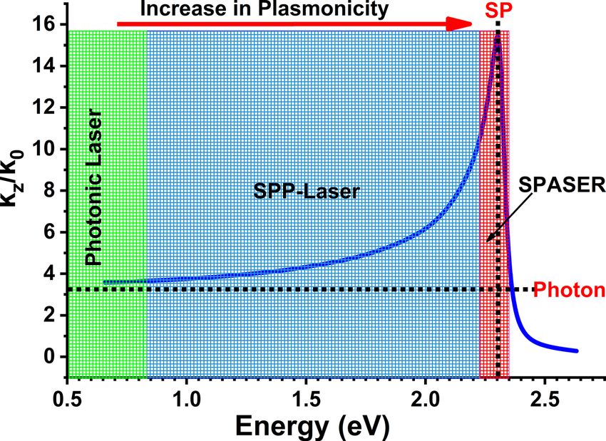
3620          C.-Z. Ning: Spaser or plasmonic nanolaser?

structure. Thus, following one of the Silicon Valley mottos: “If   meeting, when he visited me at Tsinghua in 2019, we had
you can’t beat them, buy them”, I was lucky enough to get          some extended discussions. I showed him again the disper-
Martin to join my then-new group at Arizona State to work on       sion curve (Figure 1), but with a more blurred boundary be-
the core–shell laser in 2008. The result was the demonstra-        tween the SPP-laser regime and the SPASER regime. We
tion of lasing in a similar structure, but now in an SPP mode      finally agreed that there is no difference in the essential
rather than an optical mode; the results were eventually           physics between the “SPP-laser” regime and the spaser
published in Optics Express [2] after being rejected by a few      regime (Figure 1). It is all a matter of degree in “plasmonicity”.
other journals because of the apparent similarity with Mar-        Looking back, our use of the term "plasmonic nanolasers"
tin’s earlier laser [9]. During the three to four years of our     was mostly a natural evolution of our previous nanowire-
working on the core–shell SPP laser, I had completely              based nanolasers combined with the new ingredient of SPP
forgotten about the Bergman-Stockman spaser concept [5]. I         modes. My reluctance of adopting SPASERs was also related
did not realize the close resemblance of SPP modes with the        to my incorrect perception of the spaser being at (or extremely
spaser concept initially. Nevertheless, Mark was very excited      close to) the SPP resonance (Figure 1). Mark’s original
when we met again after the Optics Express paper was pub-          comment about the absence of photons in the spaser process
lished [2]. He thought the results in the paper were proof of      in our very first meeting probably played a role also. I am
the spaser concept. I almost immediately expressed my              pleased that we were able to reach an agreement at that
disagreement with his thought. A few times at various con-         Tsinghua meeting, as it turned out to be our last meeting ever.
ferences, Mark stood up to ask me or one of my students:                Another related discussion I had with Mark involved
“why don’t you call it spaser?” My answer was always:              the acronym spaser itself; the purpose of this discussion
“because I don’t believe our device is a spaser.” The contin-      was not to challenge their creation of the acronym, but
uation of similar exchanges prompted me to consider the            primarily to confirm my understanding of the physics
similarities between the spaser and what we called a plas-         processes involved and to understand the differences and
monic nanolaser. I thought a simple dispersion relation            similarities between the spaser and the laser. My under-
would be able to convince Mark of the difference between the       standing is presented in Figure 2. I showed him an earlier
two devices. At one of the subsequent conferences, I showed        version of the lower row of Figure 2 around 2010 (see Fig. 10
Mark the SPP dispersion curve shown in Figure 1 and asked          in ref. [11]). I emphasized to him that there was no “Stim-
him: “can we agree on this distinction between the                 ulated Emission of Radiation” because there are no prop-
SPP-nanolaser and the spaser?” Mark reluctantly agreed.            agating photons (radiation) being emitted, as he told me in
Although similar arguments never occurred again, I knew            our first meeting; rather, the process is “Stimulated Energy
Mark was not fully in agreement with me. During our last           Transfer” from excited emitters to plasmons in metal

                                                                                          Figure 1: The normalized propagation
                                                                                          wavevector versus energy plot for a
                                                                                          semiconductor-silver interface; the range of
                                                                                          energy is divided roughly into three regions
                                                                                          depending on the “plasmonicity”, or the
                                                                                          degree of proximity to the surface plasmon
                                                                                          resonance (SP). We call the three regions:
                                                                                          photonic laser (conventional laser),
                                                                                          SPP-Laser, and SPASER. However, as Mark
                                                                                          insisted and I initially opposed, there is no
                                                                                          essential difference between the SPP-laser
                                                                                          and the SPASER (figure adapted from
                                                                                          Ref. [10]).
C.-Z. Ning: Spaser or plasmonic nanolaser?             3621

Figure 2: A step-by-step comparison between the conventional laser (top row) and the SPASER (bottom row) highlighting the key differences
and similarities. The green circle represents an emitter and the blue elliptical mirrors (top row) or a plasmonic metal object (bottom row). a, A:
the excited emitter (electron, the red dot, is in the upper state) in the presence of the cavity (a) or the plasmonic metallic structure (A) with
distance, d, much smaller than the wavelength, λ. b, B: Due to the presence of the cavity (b) or plasmonic metal (B), spontaneous emission into
cavity mode represented by the horizontal red arrows (b) or spontaneous energy transfer to the metallic structure to excite surface plasmon
mode (the red cloud around the blue metallic structure) (B) dominates over spontaneous emission into free space as indicated by the crossed
emission wiggles. Γpl and Γf stand for the rate of energy transfer to plasmons and that of emission into free space, respectively. c, C: The
emitter is re-excited in the presence of pre-existing cavity mode (c) and plasmonic mode (C). d, D: The pre-existing cavity mode (d) or plasmonic
oscillation (D) forces (stimulates) the excited emitter to emit the same photon (d) or plasmon (D) instead of emitting spontaneously into the
free space. The continuation of step d (stimulated emission of radiation) or D (stimulated energy transfer) eventually leads to lasing (d) or
spasing (D). For the Spaser in the lower row, we also indicate the possible far-field emission from the plasmons (red straight arrows in B, C, and
D). It is important to note that such far-field originates from the plasmon oscillation from the metallic structure, rather than from the emitter
directly. The bottom row is based on an earlier version in [11].

structures (Figure 2B, C, and D) and occurs exclusively in                 with my comment! I also expressed my opinion in my 2010
the nearfield, with no photon emission. Although I was                      tutorial [11] by using a version of a figure similar to the
joking that we should use the acronym SPASET for Surface                   lower row of Figure 2, mostly to highlight the new aspects
Plasmon Amplification through Stimulated Energy Trans-                      of the spaser. However, my intention was never to change
fer, instead of spaser, I could tell that Mark was not pleased             the acronym as I agree that the spaser is a better acronym

                                                                                                    Figure 3: Mark Stockman and I were having a
                                                                                                    conversation during our last meeting at
                                                                                                    Tsinghua University on July 12, 2019.
3622 C.-Z. Ning: Spaser or plasmonic nanolaser?
than SPASET in many senses, especially in conveying the Acknowledgment: The author thanks Alan Chin for his
similarity to the laser. Although I did not mention the careful reading of the paper and for making corrections.
SPASET term after our first discussion, I did show him the Author contributions: All the authors have accepted
comparison between the laser and the spaser as presented responsibility for the entire content of this submitted
in Figure 2 at our Tsinghua mini-symposium. I was happy manuscript and approved submission.
that we were in complete agreement about the differences Research funding: None declared.
and similarities between the laser and the spaser. Conflict of interest statement: The authors declare no
Mark was not only a brilliantly creative scholar but also conflicts of interest regarding this article.
an extremely warm and generous person. Many of us will
forever miss his big hugs. Over the years, we had many
discussions and arguments, sometimes quite heated, References
especially at the beginning of our plasmonic nanolaser
research. However, we remained very friendly and enjoyed [1] S. I. Azzam, A. V. Kildishev, R. M. Ma, et al., “Ten years of spasers
many meals together. I was very impressed with his love of and plasmonic nanolasers,” Light Sci. Appl., vol. 9, pp. 1–21,
2020.
good wines and lobster tails (I remember he ordered them
[2] M. T. Hill, M. Marell, E. S. Leong, et al., “Lasing in metal-insulator-
at least twice over the years!). I was especially happy when metal sub-wavelength plasmonic waveguides,” Opt. Express,
he told me that he was coming to China in the summer of vol. 17, pp. 11107–11112, 2009.
2019 because that allowed me a chance to meet and discuss [3] R. F. Oulton, V. J. Sorger, T. Zentgraf, et al., “Plasmon lasers at
spaser physics with him again. We, together with Renmin deep subwavelength scale,” Nature, vol. 461, pp. 629–632,
Ma, held a mini-symposium to celebrate the first experi- 2009.
[4] M. A. Noginov, G. Zhu, A. M. Belgrave, et al., “Demonstration of
mental observations [2–4] of spasers and plasmonic
a spaser-based nanolaser,” Nature, vol. 460, pp. 1110–1112,
nanolasers at Tsinghua (see the picture in Figure 3). Un- 2009.
fortunately, that meeting became our last one. [5] D. J. Bergman and M. I. Stockman, “Surface plasmon
On a lighter and more humorous note, one of our last amplification by stimulated emission of radiation: quantum
interactions involved reimbursement of his flight ticket for generation of coherent surface plasmons in nanosystems,” Phys.
Rev. Lett., vol. 90, p. 027402, 2003.
that last trip to China via wiring the money to his US ac-
[6] A. H. Chin, S. Vaddiraju, A. V. Maslov, C. Z. Ning, M. K. Sunkara,
count. After a few rounds of emails with an accountant, and M. Meyyappan, “Near-infrared semiconductor
who insisted that he must use his real name, Mark was subwavelength-wire lasers,” Appl. Phys. Lett., vol. 88, p. 163115,
frustrated and forwarded me their emails, attaching the 2006.
image of the instructions in Chinese. The instructions in [7] A. V. Maslov and C. Z. Ning, “Reflection of guided modes in a
Chinese state that the recipient must be a real person and semiconductor nanowire laser,” Appl. Phys. Lett., vol. 83,
p. 1237, 2003.
the name cannot be a “bank”, “stock”, or “security”. I
[8] A. V. Maslov and C. Z. Ning, “Size reduction of a semiconductor
immediately realized the problem, resulting in the nanowire laser by using metal coating,” Phys. Simul.
following email exchange: Optoelectron. Dev. XV, vol. 6468, p. 64680I, 2007.
[9] M. T. Hill, Y. S. Oei, B. Smalbrugge, et al., “Lasing in metallic-
Me: Mark, I found out what was wrong. It is hilarious! You have coated nanocavities,” Nat. Photonics, vol. 1, pp. 589–594, 2007.
the wrong family name that contains “Stock”. [10] C. Z. Ning, “Nanolasers: current status of the trailblazer of
Mark: Gosh, you are right! It is hilarious! Please explain to them synergetics,” in Selforganization in Complex Systems: The Past,
that I am not traded on stock markets yet as of now. Present, and Future of Synergetics, G. Wunner and A. Pelster,
Eds., Springer, 2016, pp. 109–128.
Let us hope that, with our collective efforts, one day a [11] C. Z. Ning, “Semiconductor nanolasers,” Phys. Status Solidi
company making spasers WILL be traded on stock markets! Basic Solid State Phys., vol. 247, pp. 774–788, 2010.You can also read