Special Issue on Lasers in Materials Science - Experimental Setup of Pulsed Laser Deposition at Laser Materials Processing Division, RRCAT, Indore
←
→
Page content transcription
If your browser does not render page correctly, please read the page content below
A Bulletin of the Indian Laser Association              Vol. 19, No.2, August 2008

                  Special Issue on
             Lasers in Materials Science

             Experimental Setup of Pulsed Laser Deposition at
            Laser Materials Processing Division, RRCAT, Indore
ILA Executive Committee                                           Editorial Team of
    President                                             Editor
       P.D. Gupta,                                           L.M. Kukreja                 (RRCAT, Indore)
       RRCAT, Indore
    Vice President
       V.K. Mago,                                         Editorial Board
       BARC, Mumbai                                          K. Dasgupta                  (BARC, Mumbai)
    Gen.Secy. I                                              P.K. Datta                   (IIT, Kharagpur)
       V.P.N. Nampoori,                                      S.P. Gaba                    (IRDE, Dehradun)
       CUSAT, Kochi
    Gen.Secy. II                                             P.K. Gupta                   (RRCAT, Indore)
       S. V. Nakhe,                                          A.K. Nath                    (IIT, Kharagpur)
       RRCAT, Indore                                         P. Radhakrishnan             (CUSAT, Kochi)
    Treasurer                                                H. Ramchandran               (RRI, Bangalore)
       H.S. Vora,
       RRCAT, Indore                                         P. Ramamurthy                (University of Chennai)
    Regional Representatives                                 G. Ravindrakumar             (TIFR, Mumbai)
       R. Vijaya,                                            BVR Tata                     (IGCAR, Kalpakkam)
       IIT, Mumbai                                           R.K. Thareja                 (IIT, Kanpur)
       Suranjan Pal,
       LASTEC, Delhi                                         K. Thyagrajan                (IIT, Delhi)
       Vasant Natarajan
       IISc, Bangalore                                    Editorial Working Committee (RRCAT, Indore)
       S. Khijwania,                                         Pankaj Misra       J. Jayabalan
       IIT,Guwahati
                                                             Tarun Sharma       V.S. Tiwari
       Kamal Das,
       CGCRI,Kolkata                                         Rajiv Jain         A.K. Sharma
    Corporate Representative                                 P.K. Mukhopadhyay Rakesh Kaul
       Laser Spectra Services,                               H.S. Patel         Sendhil Raja
       Bangalore

 Cover Photo :
                                                   Photograph shows the experimental setup of pulsed laser deposition
                                                   (PLD) at Laser Materials Processing Division (LMPD) of RRCAT.
                                                    rd
                                                   3 harmonics of a Q-Switched Nd:YAG laser (355 nm, 6 ns and 10
                                                   Hz) with a maximum energy of ~ 400 mJ/pulse is used to ablate
                                                   materials from their high density targets inside a vacuum growth
                                                   chamber. This ablation event produces a transient, highly luminous
                                                   plasma plume (shown in the top right inset) that expands rapidly
                                                   away from the target surface. The ablated material is condensed on a
                                                   solid substrate resulting in the formation of quantum structures or
                                                   the bulk like thin films depending upon the time and other
 conditions of deposition. The picture in the bottom left inset shows the atomic force micrograph of GaSb quantum
 dots grown on Silicon using PLD. The growth process may be supplemented by a passive or a reactive ambient and
 under optimal conditions of deposition, the ratio of the chemical composition of the target and the grown films can
 be the same. (for a relevant article please see page no. 9)
Vol. 19, No.2, August 2008                                                http://www.ila.org.in

                                             Contents
From the Editor                                                                                  1
From Indian Laser Laboratories
       Laser Based Surface Microstructuring of Lanthanum Hexaboride and                          2
       Silicon Samples for Enhanced Field Emission Effect
       Sucharita Sinha
       Ultrafast Carrier Dynamics Measurements in Reflection and Transmission Mode               3
       J.Jayabalan, Salahuddin Khan, Asha Singh, Rama Chari and S.C.Mehendale
       Sequential Pulsed Laser Deposition of Si Doped ZnO Thin Films for                         4
       Transparent Conducting Electrode Applications
       A. K. Das, P. Misra and L. M. Kukreja
Feature Articles
       Development of Novel Optical Materials for Potential Applications in                      5
       Integrated Optics and Lasers:
       R. K. Thareja
       Pulsed Laser Deposition of Semiconductors' Nanostructures                                 9
       P. Misra and L. M. Kukreja
       Laser Shock Adhesion Test (LASAT) : An Innovation Dedicated to Industry                    17
       M. Boustie, M. Arrigoni, L. Berthe, C. Bolis, S. Barradas, M. Jeandin, F. Pons and H.L. He
       Material Processing with Laser                                                            22
       R. Kaul, P. Ganesh, C.P. Paul, B.T. Rao and L.M. Kukreja
       Applications of Lasers in the Spectroscopic Characterization of                           28
       Semiconductor Bulk and Quantum Structures
       T. K. Sharma and S.M. Oak
       Raman Characterization of Materials                                                       31
       Vasant G. Sathe
Obituary
       Prof. Willis Eugene Lamb (1913 - 2008)                                                    33
Announcements
       Eighth DAE-BRNS National Laser Symposium (NLS -2008) January 7 to 10, 2009                34
       ILA Short Courses on Laser Related Topics                                                 38
       International Conference on Fiber Optics and Photonics (PHOTONICS-2008),
       December 13-17, 2008
FROM THE EDITOR....

              As we all know, research and developments in materials science have a direct
              bearing on the quality of life. And lasers have undoubtedly underpinned the
              growth of materials science in a significant way during more than last four
              decades. Followed by the early developments on conventional applications of
              lasers in materials processing such as cutting, welding, drilling and surface
              modifications etc, lasers were applied for more advanced applications in
              materials science such as pulsed laser deposition of thin films and
              nanostructures of a host of materials, in particular superconductors and oxide
              semiconductors, laser peening and laser rapid manufacturing etc. These
              developments spurred not only the growth of newer lasers with enhanced
              adaptability but also opened avenues for newer industries in the arena of
              materials engineering. Equally important are the applications of lasers for
              materials testing through nondestructive methodologies such as holography,
              speckle interferometry etc. These methodologies have helped materials
              scientists to understand the properties of materials under different conditions of
              their applications. Keeping such an important contribution of lasers in the field
              of materials science in view, we have dedicated this issue of Kiran to this theme.

              Besides the thematic articles of this special issue, we have our usual features
              ‘from Indian Laser Labs’, announcements about the forthcoming conferences
              like Photonics 2008, National Laser Symposium (NLS - 08) and the short
              courses for young scholars being organized by Indian Laser Association prior to
              NLS - 08. I hope you will find this issue of ‘Kiran’ both interesting and
              informative.

              For the laser community it is saddening to note that Prof. Willis Eugene Lamb is
              no more. He passed away on May 15, 2008. Prof. Lamb’s contributions to laser
              physics are foundational and historical. He was honored with Nobel Prize in
              1955. On the last page of this issue we pay our homage to this great scientist and
              a perfectionist.

              Lalit M. Kukreja
              August 8, 2008

                                        1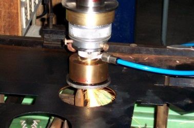
From Indian Laser Laboratories

     Laser Based Surface Microstructuring of Lanthanum Hexaboride
         and Silicon Samples for Enhanced Field Emission Effect

      A novel technique of Laser based surface          such laser treated samples have shown enhanced
microstructuring has been successfully                  field emission effect with good emission stability,
demonstrated at Laser and Plasma Technology             high current density and low turn on field, largely
Division, BARC in collaboration with                    confirming that these improved field emission
Department of Physics, University of Pune. This         characteristics are due to the dense array of
simple single step laser ablation technique leads       spontaneously aligned microstructures generated
to formation of periodic ripples and an array of        through the process of laser surface irradiation
self aligned conical columnar structures on the         and associated field enhancement at these micro-
laser treated surface. These spikes or micro-           tips.
columnar periodic surface features having sub-
                                                        (a)
micron tip diameter have been observed to work
as high current density emission cathodes
operating at low voltage similar to micro-tip
arrays, having potential application in micro-
electronics as cold cathode field emitters.

     Scientists at L&PTD, BARC used a mode-
locked pulsed picosecond Nd:YAG laser
operating at its second harmonic wavelength of
532nm, delivering laser pulses of 35picoseconds
pulse duration and pulse energy of 20mJ to
demonstrate this process of laser based surface
microstructuring. While, use of Lanthanum
Hexaboride as an excellent electron source has
been widely reported for its high brightness and        (b)
long life, Silicon too has been extensively
investigated as a potential cold cathode electron
source largely because of easy integration of
Silicon tips to existing Silicon based
microelectronic devices.

      Lanthanum Hexaboride and Silicon pellets
were subjected to laser treatment under a vacuum
of about 10-2 mbar, for varying exposure times.
Using appropriate focusing optics the incident
                                                2
laser fluence was varied over a range of 0.5J/cm
            2
to 10J/cm for both the samples. Surface
microstructure and morphology of these laser
treated samples were subsequently examined
under a Scanning Electron Microscope (SEM).                   Fig.1 SEM Image of Laser treated
                                                              (a) Lanthanum Hexaboride, and (b) Silicon.
Typical SEM images of laser treated Lanthanum
Haxaboride and Silicon samples showing conical
microstructures are shown in Fig.1. Field                                             Sucharita Sinha
emission measurements when performed with                         Laser and Plasma Technology Division
                                                                        Bhabha Atomic Research Centre
                                                                                      Mumbai-400 085

                                                    2
From Indian Laser Laboratories
Ultrafast Carrier Dynamics Measurements
in Reflection and Transmission Mode
Measurements of photo-induced and reflectivity measurements in solid and liquid
transmission or reflectivity can provide samples. The output of a 100fs, 82 MHz Ti:
information about the carrier dynamics in metal Sapphire laser is split into a strong pump and a
and semiconductor quantum structures. In metals weak probe which are then spatially overlapped
the absorption of incident light causes a smearing on the sample with a variable time delay between
of the Fermi-surface, which modifies the inter- them. The maximum time delay is usually
band and intra-band absorption. In restricted to 200 ps but can be extended up to 1 ns
semiconductors photo-generated carriers induce a if required. Mechanical chopping of the pump and
change of absorption due to effects like band lock-in detection of the probe enables
filling, band gap renormalization, screening and measurement of small changes in the transmission
free-carrier absorption. In a pump-probe or reflectivity of the sample. Figs 1 and 2 show
configuration the pump pulse induced changes in examples of transient transmission and reflection
absorption cause a modification of the refractive measurements done in our lab. We collaborate
index, which in turn changes the transmitted or with groups developing novel nanostructured
reflected energy in the probe. By monitoring the materials.
sign, magnitude and recovery time of these
changes it is possible to study electron-electron
and electron-phonon scattering in metals, while in
semiconductors carrier capture, carrier cooling
and carrier decay can be studied.
In our lab we have installed a pump-probe
set-up for measurement of transient transmission
Fig 2. The transient changes in the reflected
intensity of a quantum well sample at two
different pump powers. The reflectivity change is
negative and shows a fast and a slow component.
J.Jayabalan, Salahuddin Khan,
Asha Singh, Rama Chari and S.C.Mehendale
Fig 1. The transient changes in the transmission of
metal nanoplatelet colloid for different pump powers. Laser Physics Applications Division
To reduce the possibility of thermal degradation the Raja Ramanna Centre for Advanced Technology
sample was kept under constant flow through a 1 mm Indore 452013
cell. For 10 mW pump power the decay time is 710 fs.
3From Indian Laser Laboratories
Sequential Pulsed Laser Deposition of Si doped ZnO Thin
Films for Transparent Conducting Electrode Applications
Sequential pulsed laser deposition was used found to decrease drastically with Si doping and
-4
to grow highly oriented Si doped ZnO thin films reach a minimum value of about 6.2×10 ohm-
with different Si concentrations on (0001) single cm. Carrier concentration was also found to
20 -3
crystal sapphire substrates for use in transparent enhanced and reach a value of about 3×10 cm
conducting electrode applications. The compared to the value ~ obtained for undoped
composition of the films was varied by ZnO film. All the films were highly transparent up
controlling the ablation time of Si target to ~ 80% in visible spectral region (400-800nm)
compared to that of the ZnO target. The Si for all the compositions as seen in figure 2.;
ablation time was kept fixed at 1 sec while ZnO however the absorption edge of ZnO was found to
ablation time was varied in the range of 10 to 50 shift monotonically towards blue with increasing
sec to get different concentrations of Si in ZnO. Si doping. The increase in the bandgap of ZnO
these sequences were repeated in predefined way with Si doping was explained by considering the
to achieve nearly same film thicknesses of ~150 competing effect between Burstein-Moss shift
rd
nm. The 3 harmonic of a Q-switched Nd:YAG and band gap renormalization due to high carrier
laser at a fluence of ~1 J/cm2 was used for the concentration. The highly transparent and metal
ablation. The substrate temperature was like conducting Si doped ZnO films have the
o
maintained at ~600 C to facilitate proper doping potentials to be used as transparent conducting
of Si in ZnO. electrodes in display panels, solar cells and
organic semiconductor based electronic and
The deposition chamber was evacuated to a photonic devices.
-6
base pressure of 1×10 mbar prior to deposition
and then filled with oxygen ambient up to a
pressure of ~ 1×10⁻⁴ mbar during the deposition.
EDX measurement showed that the Si content in
the films increased monotonically with increasing
Si ablation time compared to that of ZnO. the
resistivity of the films shown in figure 1,was
Fig 2: Transmission spectra for different
Si to ZnO ablation duration ratio
A. K. Das, P. Misra and L. M. Kukreja
Laser Materials Processing Division
Fig 1: Variation of resistivity with Raja Ramanna Centre for Advanced Technology
Si to ZnO ablation duration ratio
Indore 452 013
4Feature Article
Development of Novel Optical Materials for
Potential Applications in Integrated Optics and Lasers
The main driving force behind such efforts oxides and nitrides for potential applications as
has been the development of blue-green diodes lasing and nonlinear medium for short
and lasers for optical recording and optical wavelength lasers, 1-d photonic crystal
waveguides, not with standing several other applications (multilayer -films) e.g; Zn1-x MgxO,
applications such as printing, communications, SiO2, and Al2O3, UV sensors (band-gap
and various sensor applications. In optical engineering-extend cutoff wavelength from UV-
recording systems, information is recorded in bits A (320-400nm) to UV-B (280-320 nm)) for use in
and read by a semiconductor laser whose output is radiation monitoring, ultra-high temperature
focused to a diffraction-limited spot. A significant flame detection, and airborne missile warning
gain in recording density as well as data transfer systems. We have recently demonstrated laser
rate can be achieved by simply using lasers (micro action in UV in ZnO nanocrystalline films. Figure
lasers) that operate at shorter wavelengths. The 1 shows laser action in pulsed laser deposited ZnO
key issue of the micro laser is to confine light in a thin film. Figure 2 shows Bandgap variation of
small volume with dimensions of the order of Mg0.1Zn0.9O and Mg0.3Zn0.7O films with substrate
optical wavelength. The fabrication of these lasers temperature.
requires expensive state of the art crystal growth
and micro- fabrication facilities. The current
research effort has been on making nonlinear
optical wave-guides of LiNbO3 and KPT.
However, these wave-guides are made from
expensive single crystals facilities.
Fig. 2
Pulsed laser ablation
The use of LIBS as an analytical tool has
considerably grown over the past 10 years. Being
based on laser-induced plasma that can be
produced in all most all media e.g. gas, liquid,
conducting or non-conducting solids, LIBS can
be regarded as a unique sampling, atomization,
excitation and ionization source. One major
advantage of LIBS analysis over other methods is
Fig. 1 that the spatial information for the distribution of
Therefore, it is desirable to look for elements is preserved. Thus has potential for the
alternatives like thin films with large non- linear analysis of minerals and potentially toxic
response. Our emphasis has been on investigating elements within calcified tissue e.g. teeth and
laser deposited nanocrystalline thin films of bones, and dental materials. Using the technique it
5should be possible to distinguish unequivocally 3
p-3p at 507.8 nm) is observed in the emission
between healthy and caries infected teeth. The spectrum of laser-ablated aluminum plasma at 70
technique can also be applied to trace the temporal Torr nitrogen ambient 6-8 mm away from the
evolution of pollutants in environment. We have aluminum target. A one-to-one correlation
studied titanium (Ti), silicon (Si), zinc (Zn), lead between the reaction enthalpy and the laser
(Pb), carbon (C), and aluminum (Al) etc, the fluence was observed, more endothermic the
elements that are important to medical, biological reaction higher is the fluence required for the
and environmental exposure studies. For formation of nitrides and oxide compounds.
example, chronic accumulation of lead and Figure 4 shows Optical emission spectrum of
aluminum in the body may affect the inner organs. aluminum plasma in ambient atmosphere of
In order to visualize the behavior of the selected nitrogen at 1 mTorr and 70 Torr. Inset shows AlN
atomic and molecular species, we have used a band with maximum intensity observed at an
combination of the laser spectroscopy with an ambient pressure of 70 Torr and 8 mm away from
imaging technique. In addition to optical emission the target. Figure 5 shows spatially resolved
spectroscopy, laser induced fluorescence (2-D emission spectrum of CN band at 0.1 Torr of
imaging) is being used for Spectroscopic ambient nitrogen pressure at fluence of 12 Jcm .
-2
applications (Spectro-chemical analysis, Species Inset shows time integrated spectrum of CN
in various states: carbon, aluminum, copper etc. bands. The ICCD imaging of the expanding
The technique can be used for Biomedical plasma using fast photography showed instability
applications (Imaging: spectral and microscopy at the plasma-gas interface, quantified as the
and Horticulture (Quality of fruits) applications. Rayleigh-Taylor instability with growth time of
The LIF technique allows the detection of ground instability estimated in the range 0.09 to 4 ms. Fig.
state or long-lived, non-radiative, excited-state
atoms, molecules or radicals. Figure 3 shows C2
and C3 LIF images at various ambient pressures of
N2 gas
Fig. 3
In recent years we have extensively studied Fig. 4
the pulsed laser-ablation of aluminum, carbon,
and titanium plasma in nitrogen and oxygen
ambient to understand the formation of AlN, CN,
and TiO using optical emission spectroscopy,
plume dynamics of the expanding plasma,
instability, mechanism and estimation of the
strength of self-generated magnetic field using
fast photography, and anisotropic emission in the
laser-ablated plasma using both space- and time-
resolved optical emission spectroscopy with
nanosecond and picosecond laser pulses.
Formation of AlN band (0-0 band head transition
Fig. 5
66 shows Al plasma expanding in nitrogen and 9 ´ 105 K at 0.1 Torr and 1.6 ´ 106 cm s-1, 2.3 ´
ambient. Fig 7 (a) shows shock wave formation at 107 Nm-2, and 1.6 ´ 105 K at 70 Torr, respectively,
0.1 Torr, and (b) RT instability at plasma-gas at a delay time of 160 ns. However, at pressures of
interface at 1 Torr ambient nitrogen pressure and 10 and 70 Torr V and Tv showed an oscillatory
300 ns delay time. behavior at delay times greater than 260 ns. The
In order to understand the plasma dynamics oscillatory behavior is attributed to the occurrence
from images we used the shock wave model of the of instability in the plasma that grew at later stages
n
form R = at where a is a constant, and drag model of expansion.
-bt
of the form R = Ro(1–e ) relating the distance of For the first time an attempt is made to
plasma plume front R at different delay time t with estimate the strength of the self-generated
respect to the laser pulse , where Ro is the stopping magnetic field B in the plasma near the focal spot
distance (distance at which the plume comes to using ICCD images and was found to be around
rest), and b is the stopping coefficient. 26 kG. Steep pressure gradient at the plasma-gas
interface seems to be the cause that generates
these fields. An attempt is made to study the
polarization of plasma at various background
pressures and incident laser energies. The
polarization, alignment of the ions in specific
upper level results from spatial anisotropy of the
plasma. Since our plasma is optical thin, the origin
of this alignment could be spatially anisotropic
velocity distribution arising due to Maxwellian
distribution with different temperature in
Fig. 6
Fig. 7
Hydrodynamic equations are used to
calculate the vapor density, vapor pressure (Pv),
and vapor temperature (Tv), respectively, just
behind the plasma front. Velocity (V), Pv, and Tv
were found to be 3.8 ´ 10 cm s , 1.8 ´ 10 Nm ,
6 -1 5 -2
Fig. 8
7different directions. Therefore, degree of
polarization is a measure of anisotropy in the
electron distribution function in laser-induced
plasmas. It is defined as P = (III-I^)/(III+I^) where III
is the intensity of the laser light whose component
is parallel to the plane of laser incidence and I^ the
intensity perpendicular to the plane of laser
2
incidence. We used Al III transition 4s S1/2 – 4p
2 o
P 3/2 at 569.6 nm to measure P. Figure 8 shows the
polarization resolved images and spectrum of
horizontal and vertical components of Al III
plasma emission at 0.1 Torr ambient pressure of
nitrogen. The degree of polarization Fig. 9
measurements for Al III transition 4s 2S1/2 – 4p 2Po3/2
at 569.6 nm showed pulse width dependence i.e.
more anisotropy with picoseconds laser pulse as
ambient atmosphere of inert gas.
compared to that with nanosecond laser pulse.
The evolution of cluster size is obtained by
In order to study shocks generated due to low
incorporating diffusion of ambient gas into an
intensity irradiation pump-probe experiments
adiabatically expanding plume. The onset time
where plasma forms one arm of the Mach-
dependence on ambient pressure follows a simple
Zehnder Interferometer (MZI) are carried out.
relation of the form {}. The reasonable agreement
The plasma is produced using ns pulse whereas 35
of simulated results for Si with experimental
ps laser (green) is used to temporally probe the
observations implies that model is adequate to
plume. The interferograms and shadowgrams are
simulate Si cluster formation in the ablation
recorded on CCD-camera kept perpendicular to
plume.
the target surface. From the fringe shift we
estimate electron density of 7 x 1018 cm-3 in The work reported is supported by IITK,
ambient air. The radial density contours are DST and DRDO.
converted in to axial variation of density using
Abel inversion technique. Figure 9 show s typical
pump-probe experimental lay out. Recently R. K. Thareja
preparation of nano-particles by laser-ablation Department of Physics &
has gained lot of interest because of its advantages Center for Laser Technology
over other methods for creating nanoparticles. Indian Institute of Technology,
We have developed a simple model to simulate the Kanpur-208016
clusters formation in laser ablated plume in an
8Pulsed Laser Deposition of
Semiconductors’ Nanostructures
Introduction non-availability of reliable short pulse laser with
suitable peak power, wavelength and repetition
Pulsed Laser Deposition or PLD for short is
rate, which resulted in the non-congruent
an advanced application of lasers in materials
evaporation of material and inferior material
science. PLD is a versatile and perhaps one of the
quality of the grown films using Pulsed Laser
simplest growth methodologies to deposit thin
Deposition (PLD) specially as compared to those
films and quantum structures of variety of
grown by other well established techniques such
materials using high power lasers [1-3]. The high
as Molecular Beam Epitaxy (MBE) and Metal
power laser pulses are used to ablate materials
Organic Chemical vapor Deposition (MOCVD)
from their high density targets in vacuum. This
etc. With the advancement of laser technology
ablation event produces a transient, highly
during initial years of 1970 – 80 and development
luminous plasma plume that expands rapidly
of Q-switched lasers to produce short duration
away from the target surface. The ablated material
pulses with high peak power the congruent
is condensed on a solid substrate resulting in the
evaporation of complex materials could be
formation of quantum structures or the bulk like
demonstrated successfully [5]. This was and still
thin films depending upon the time and other
one of the major advantages of this technique.
conditions of deposition. The growth process may
Another visible achievement in this sequence,
be supplemented by a passive or a reactive
which accelerated the PLD activity, was the
ambient and under optimal conditions of
availability of short wavelength lasers such as
deposition, the ratio of the chemical composition
excimer lasers or conversion of IR wavelength
of the target and the grown film can be the same.
through the process of second and third harmonic
Despite its inherent problems of particulates and
generation such as that from Nd:YAG lasers. The
large area scaling, PLD has emerged as a popular
major outcome of a short wavelength laser was in
choice for the growth of complex oxide materials
the considerable reduction of micron sized
mainly due to its extreme simplicity, congruent
particulates on the film surface which was a
evaporation and ease in handling reactive oxygen.
serious problem in the case of long wavelength
laser due to large absorption depth of the laser
light in the material. Subsequently the concept of
Historical Background and Evolution of PLD laser deposition in presence of a reactive
The efforts toward using Lasers in environment, established by Gapanov et al added
depositing thin films started soon after the further value to the methodology of PLD [6]. The
invention of reliable high power lasers. Early gas phase reactivity was found to enhanced due to
observations of the ease with which the material high kinetic energy of the ablated species which in
3
could be vaporized by the intense interaction of the range of ~1 – 10 eV [7]. Even today this is
high power laser pulses with material surface considered a unique feature of PLD. The advent of
demonstrated that the intense laser radiation could ultra-short pulse (femto-second) lasers has
be successfully used to deposit thin films of that enabled new insights into the realm of PLD [8].
material. In 1965 Turner and Smith [4] were the However the Ultra-short laser ablation physics is
first to demonstrate deposition of thin films using drastically different from that of conventional
high power Ruby laser. Although the work nanosecond laser ablation and a complete
performed by them was mostly exploratory, it understanding of the processes involved is still to
demonstrated the feasibility of thin film be emerged.
deposition using a pulsed laser. Scanty progress Realizing the importance of PLD for the
was noticed in this field until 1970 mainly due to growth of broad range of nanostructured materials
9for multitude of areas of science and technology, surface of target material. Interaction of
we have created PLD facility at our center during evaporated cloud with the incident laser beam
1998. One of our early goals was to be able to use results in cloud heating and plasma formation.
this technique to grow structures of nanometer Although the laser evaporation for the deposition
size with control on shape, dimensionality, size of thin films occurs at much lower power
and size dispersion etc, which was rather an densities, the plasma temperatures can be as high
4
intricate problem. At the incipient stages of as ~10 K [1, 2]. This plasma cloud Expands in to
‘nanofabrication’ of structures, materials vacuum or in an ambient atmosphere a very high
5 6
scientists were understandably apprehensive expansion velocity, of the order of 10 -10 cm/sec
about the use of PLD for growing nanometer size [7] and kinetic energy ~ 10-1000 eV. The laser
structures primarily because of its inherent ablated plasma plume is allowed to condense on a
limitations of this technique i.e. particulate substrate, which is mounted on an electrical
production and large average thermal energy of heater to control its temperature during the
the plume resulting from laser ablation of the deposition of the nanostructures. Since the laser
target material [1]. However, amongst other ablation results in congruent evaporation, multi
groups, we took this as an interesting scientific component materials can be deposited with nearly
exercise to devise and evolve ways of growing the same stoichiometry as in the target. Secondly,
nanostructures of deterministic characteristics the rate of evaporation per pulse is so low that one
using PLD. We have shown that despite its innate can deposit a layer with control on thickness as
limitations there is an optimized regime of growth fine as 0.1Å per pulse.
parameters in which this technique can indeed be
applied for fabrication of high quality
nanostructures.
Experimental Setup and Methodology
The PLD system developed at our laboratory
is shown in Fig. 1. It consists of a commercial
(Quantel make) Q-switched Nd:YAG laser
capable of providing 6ns laser pulses at variable
repetition rate up to10 Hz with energy per pulse up Fig. 1 : Schematic of the pulsed laser
to 1.6 J in fundamental (1.06 µm), about 800 mJ in deposition setup developed at RRCAT, Indore
second harmonic (533 nm) and 450 mJ in third
This deposition process is carried out in two
harmonic (355 nm). At these energies and pulse
different growth chambers, which are first
duration practically every known material on -6
evacuated to a base pressure of 10 Torr in case of
earth can be ablated to generate its plume. -9
one chamber and 10 in the other one, using a
However for all practical purposes we use the
turbomolecular pumps and can later be filled with
third harmonic of this laser because at the shortest
flowing gaseous ambient required for different
wavelength the absorption of the radiation is the
deposition conditions. The gaseous ambient may
highest and the plume is particulate free. In
be required for example, for obtaining
general when an intense laser beam is zapped on
stoichiometric composition of the deposited
to the solid targets some part of it is lost due to
structure or for supplying the species for doping
reflection, scattering etc. and the rest is absorbed
purposes. Since laser beam can pass through a
up to a certain depth into the target material, also
gaseous ambient, PLD works as good in the
known as absorption depth. The absorbed laser
presence of a gaseous ambient as in vacuum. The
energy is spent in intense localized heating of the
growth chambers are provided with a number of
target resulting melting and/or vaporization of the
102
electrical feed-throughs for supplying electrical at two different fluences of ~100 and 1250 J/m is
power to the substrate heater or for monitoring the shown in Fig. (a, b). At low laser fluence of ~100
substrate temperature online. After deposition of J/m2 , as shown in Fig. (a), only atomic and
the nanostructured materials their properties of diatomic Zn are present in the ablated plume.
interest are studied using a cornucopia of Most other signals in the low-mass range
characterization facilities like scanning probe represent salt ions resulting from unintentional
techniques, X-ray techniques, photoelectron impurities present in the ZnO target. Cluster
spectroscopy, Raman and magnetic techniques formation is not visible in the mass spectrum at
etc. mainly at other laboratories through this low fluence but molecular ZnO and Zn2O can
collaboration. be seen with low intensity. However the ZnO
cluster formation enhanced significantly with
increasing laser fluence. Fig. (b) shows this for a
2
Research Areas and Findings fluence of 1250 J/m . This mass spectrum
contains a complete series of (ZnO)n clusters up to
During last about one decade we have
pursued research on nanostructures of myriad of sizes (n) ~ 20. For cluster sizes up to about 10,
materials, the choice of which was swayed twin signals are identifiable, one peak
towards the relevance to the advanced corresponding to clusters of equal numbers of
technologies being pursued at our organization. zinc and oxygen atoms, and an additional peak
In this article we present our recent research corresponding to clusters with an added zinc
results and findings on semiconductor atom. The relative intensity of the latter species
nanostructures suitable for UV-visible photonic drops with cluster size. In addition, clusters with
devices. These material structures include two additional zinc atoms are formed up to n = 3.
multiple quantum wells of ZnO and quantum dots
of ZnO and Si in multilayer fashion. The findings
of our research in this field have been published in
a number of papers in peer reviewed journals and
in international conference proceedings. A
glimpse of our research findings in pertinent area
can be obtained from the representative sub-
domains, which are as follows:
Composition of Laser Ablated ZnO Plume and
Cluster Formation
Cluster physics is an important ramification
of nanoscience. One of the mechanisms of the
formation of clusters is the gas phase
condensation and this occurs in the laser ablated
plumes of the target materials also. We have
studied the composition of nitrogen laser
(wavelength: 337nm, pulse width: 3ns) driven
ablation plumes from ZnO target at different
fluences using a time-of-flight mass spectrometer
(TOF-MS) [9] and found that the ablation plume
contains very complex species ranging from
atoms to clusters with a distribution, which is
Fig. 1 : Time-of-flight mass spectra of ZnO
highly dependent on the laser fluence used. The
ablation plumes recorded in positive-ion mode
mass spectra of ZnO plume in positive ion mode
at fluences of (a) 100 J m-2 and (b) 1250 J m-2
11-5
Besides its value for understanding the ambient at a partial pressure of ~ 1x10 Torr. The
fundamental nature of the cluster formation, these average growth rate at the aforesaid fluence was
studies have important implications for the PLD found to be ~ 0.1 nm/sec for ZnO and ~ 0.08
grown nanostructures. If at a laser fluence nm/sec for MgZnO [13]. The Mg concentration in
formation of stable clusters (with magic peaks) the PLD grown MgZnO films was found to be ~
initiates, that fluence has to be excluded for the 34% using energy dispersive X-ray analysis
growth of the nanostructures free from such (EDAX). Prior to the growth of the MQWs a 50
clusters. nm thick ZnO buffer layer was grown on the
substrate at 750ºC. This buffer layer provided
ZnO Quantum Wells
highly crystalline, relaxed and smooth surface of
Currently ZnO, with its direct band gap of the ZnO template on sapphire for subsequent
about 3.3 eV at room temperature, is of immense growth of the high quality MQWs at lower
interest for blue and ultra-violet (UV) photonic temperatures [14]. Ten periods of ZnO/MgZnO
devices such as light-emitting diodes, laser MQW structure were grown at 600ºC. The barrier
diodes, solar blind UV photodetectors, etc. Its layer thickness was kept constant at ~ 8 nm while
large exciton binding energy of ~ 60 meV allows the ZnO active layer thickness was varied from ~
the excitonic transitions at room temperature. 4 to 1 nm to grow MQWs of different well layer
Besides this, ZnO is a well-known rugged and thicknesses with in-plane size of about 5mm x
radiation hard material for oxygen gas sensors, 5mm.
Surface Acoustic Wave devices, Varistors,
Optical absorption spectra, taken at room
Resonant Tunneling Devices, transparent
t e m p e r a t u r e ( R T ) u s i n g a U V- V I S
conductors, and UV screens etc [10-12]. The
spectrophotometer, are shown in fig. 3. These
evolution of next generation photonic devices and
spectra revealed an average transmission of ~80%
sensors etc. necessitates research on quantum
in the visible region for all the MQW samples. The
structures of ZnO. Among other quantum
absorption spectra of ~200 nm thick films of ZnO
structures the two dimensional quantum wells are
and MgZnO show their band-edges at expected
of particular importance due to their fascinating
~3.3 and 4.1 eV respectively along with the
size dependent physical properties such as large
conspicuous excitonic humps. Each absorption
oscillator strength of optical transitions, enhanced
spectrum of the MQWs consists of three well
excitonic binding energy, tunability of operating
resolved features. The broad shoulders at ~ 3.3
wavelength, very low threshold of lasing and
and ~4.1 eV obviously correspond to the ZnO
quantum transport properties. We have grown
buffer layer and the MgZnO barrier layers
high quality ZnO/MgZnO multiple quantum
respectively. It is noteworthy here that the
wells (MQWs) using pulsed laser deposition
constant position of the absorption edge
(PLD) on epi-polished (0001) sapphire substrates
corresponding to the barrier layers of MgZnO in
with r.m.s. surface roughness of ~ 0.3 nm. Third
all the MQW samples is indicative of negligibly
harmonic of a Q-switched Nd:YAG laser
small inter-diffusion of chemical species at the
operating at 355 nm, 10 Hz with 6 ns pulse width
2 ZnO/MgZnO interfaces. The central peaks in
was used at a fluence of ~ 0.6 J/cm to ablate
these absorption spectra are found to correspond
alternatively the sintered pallets of ZnO and
to the n=1 excitonic transition of the ZnO
MgZnO used as targets in the PLD growth
quantum wells. It can be seen that this peak
chamber. The MgZnO target consisted of calcined
undergoes monotonic blue-shift with decreasing
mixture of 10 mole % of high purity MgO and
well layer thickness from 4 nm to 1 nm as
remaining ZnO. The growth chamber was
-7
expected from the quantum confinement effects
initially evacuated to a base pressure of ~1x10 [15].
Torr using a turbo-molecular pump and
depositions were carried in high purity oxygen The photoluminescence (PL) studies of the
MQWs were carried out in two separate
12experiments. One study was carried out at our peaks increased monotonically with decreasing
laboratory using the HeCd laser (wavelength: 325 active layer thickness. This was attributed to the
nm) as an excitation source for MQWs with well fluctuations in well layer thickness and
layer thickness up to 1.5 nm, the results of which dominance of the interface roughness in thinner
are shown in fig. 4. This excitation source was not wells. Along the vertical progression of the PL
able to excite the MQWs of shorter well layer peaks in fig. 9 it can be observed that for a
thicknesses because the quantum confinement particular well layer thickness of 2.5 nm, as the
shift in them pushed the band-gap to energies temperature of the MQWs is increased, the PL
larger than the photon energy of the HeCd laser peak not only broadens but it also shows a
(about 3.8 eV). Therefore we used an ArF monotonic red shift. While the increase of the PL
Excimer laser (wavelength: 193 nm) for the line width was attributed to the exciton scattering
MQWs of shorter well layer thicknesses, the with the acoustic and LO phonons, the red shift
results of which are shown in fig. 4. was explained using Varshni’s empirical relation
of the band gap shrinkage with increasing
Along the horizontal progression of the PL
temperature [16]. The PL from ZnO MQWs of
peaks in fig.4 it can be seen that as the well layer
well layer thickness shorter than 1.5 nm was
thickness was decreased from ~ 4 nm to 1.5 nm
recorded by using 193 nm excitation source of
the PL peaks shifted from ~3.36 to 3.67 eV. It can
ArF Excimer laser at 10 K in conformity with the
also be seen in this figure that the width of the PL
size dependent spectral shift [17]. The band-gaps
of the MQWs of different well layer thicknesses
obtained from these PL studies at 10K are shown
in inset of fig. 4. To understand the observed
functional dependence, we calculated the ZnO
QW band gap at different well thicknesses by
solving the time independent Schrödinger
equation using square potential well
approximation [15]. The calculated values are
shown by the dotted curve in fig. 4. One can see a
reasonable agreement of the theoretical curve
with the experimental values obtained from the
PL data. Armed with this growth methodology
Fig. 3 : Optical absorption spectra of ZnO MQWs and
200 nm thick films of ZnO and MgZnO at RT. The values
and the band-gap data, one can deploy these ZnO
in the parentheses show the respective band gaps in eV. MQWs for a host of device and research
applications.
ZnO Quantum Dots
The evolution of next generation photonic
devices and sensors etc. necessitates research on
quantum dots of ZnO. Research on quantum dots
(QDs) of ZnO is particularly interesting for the
development of nano-regime sensors, catalytic
and other chemical systems (for example ZnO
QDs are known to remove arsenic from water)
and photonic devices etc. We have grown
Multilayer matrices of ZnO Quantum Dots (QDs)
Fig. 4 : Photoluminescence peaks form ZnO of different sizes in the range of ~ 2 to 4 nm
MQWs for different well layer thickness and embedded in alumina layers on optically polished
temperatures. Inset shows bandgap vs. well thickness.
sapphire substrates by using the same set-up as
13that for the growth of ZnO MQWs. The laser
2
fluence in this case was kept at ~ 4 J/cm to ablate
the sintered targets of Al2O3 and ZnO alternately.
The deposition was carried out in the oxygen
"2
ambient at a pressure of about 10 Torr and the
substrate to target distance was kept at ~ 4 cm.
Prior to the deposition of the ZnO QDs an ~ 10 nm
base layer of alumina was grown on the
substrates. On this base layer were grown the
randomly distributed QDs of ZnO by the
condensation of the ablation plume through a
mechanism, which is yet to be fully understood.
This layer of the QDs was then capped with Fig. 5 TEM micrograph of ZnO quantum dots (QDs).
Upper left inset shows the AFM of these QDs and lower
alumina.10-layer structure of ZnO QDs and
right inset shows the selective area diffraction pattern.
alumina capping layer was grown by the alternate
ablation of the respective targets. The capping
layer of alumina was grown for 30 s in all the
samples and the deposition time of the ZnO DQs
layer in different samples was taken to be 3, 5, 7,
10 and 15 s. We have investigated its structural
and optical properties [18, 19] which are
discussed below.
Fig. 5 shows the in-plane dark field
Transmission Electron Microscope (TEM) and
AFM micrographs of the ZnO QDs grown by
PLD. Selective area diffraction pattern (also
Fig. 6 Variation of the band gap as a function of the mean
shown in fig. 6) was fitted with the theoretical
quantum dot radius. Experimental data are shown by
values, which confirmed that these QDs were full circles with variation in the size by horizontal bars
actually that of ZnO. From the TEM micrographs
we calculated the mean size and size distribution excitons can exist and therefore the coulombic
of the QDs deposited at different times. From the interaction term is replaced by the excitonic
optical absorption studies we calculated the band- binding energy. The calculated values of the band-
gaps of the QDs of different sizes. These gap in this case [21] are shown by the ‘weak
experimental values of the band-gaps as a confinement’ curve in fig. 6. Good fit of the
function of the mean QD radius are shown in theoretical curves with the experimental values is
fig.6. To explain these data we proposed two indicative of the efficacy of our model.
confinement domains. In the size domain where
the dot size is smaller than the excitonic Bohr Silicon Quantum Dots
radius (calculated to be about 2.2 nm) it is
As we all know, Silicon (Si) is the mainstay
plausible that the exciton may not exist and
material of the contemporary electronic industry.
therefore holes and electrons will experience a
But because of its indirect band-gap, which under
strong confinement with a characteristic reduced
normal circumstances prevents light emission,
mass and a coulombic interaction. Under this
applications of Si in photonic devices are limited.
circumstance, the calculated values of the band-
However the observation of strong luminescence
gap [20] are shown by the ‘strong confinement’
in UV-Visible spectral range from Si
curve in fig.6. On the other hand when the dot size
nanoparticles makes them a promising option for
is greater than the excitonic Bohr radius the
photonic applications. Recent observation of
14optical gain in Si nanoparticles embedded in SiO2 grow nanoparticles with extremely narrow size
matrix also opens up a possibility of adding Si dispersion. Efforts are also underway to grow
based optically functional devices on the existing multi-layer matrix of Si nanoparticles embedded
Si microelectronic circuits [22]. Consequently in SiO2 or other suitable host materials suitable as
currently there is worldwide interest in growing Si optical gain media.
nanoparticles and studying their characteristics.
We have grown Si nanoparticles using a novel in-
house developed methodology of off-axis PLD Conclusions
[23]. This methodology was found to be very
effective in preventing the deposition of micron In conclusion, we have used in house
size chunks amongst Si nanoparticles as observed developed PLD setup to grow high quality
in normal PLD [23]. A schematic of the off-axis semiconductor nanostructures. The efficient PL
PLD geometry is shown in the inset of fig. 7. obtained from ZnO multiple quantum wells
grown by us using highly optimized buffer
assisted PLD methodology indicates that PLD
can be used for the production of ZnO based
photonic and transparent electronic devices. PLD
was also used to grow multilayer matrices of ZnO
and Si quantum dots wherein size dependent blue
shift was observed due to putative quantum
confinement effect. Thus PLD is well suited for
the growth of semiconductor nanostructures in
controlled fashion.
Acknowledgements
The research and development work
Fig 7 Transmission spectra of (a) sapphire substrate and recounted in this article is the produce of
multilayer matrices of Si nanoparticles grown for teamwork carried out with our colleagues and
different times of (b)30 (c) 120 (d) 180 and (e)240 sec. collaborators from our centre, UGC-DAE Centre
Optical absorption spectra of the Si for Scientific Research and Universities of
nanoparticles of different sizes, recorded at room Muenster and Ulm, Germany.
temperature with a wavelength resolution of 2 nm
in the spectral range of 200-1500nm and are
shown in figure 13. The absorption spectrum of References
the reference sapphire and that of bulk Si were 1. Pulsed laser deposition of thin films edited
also recorded separately (also shown in fig. 13) to by Douglas B. Chrisey and Graham K.
ensure that they did not have any absorption Hubler; John Wiley & Sons, Inc., New York
feature in the spectral range of interest. It can be 1-19 (1994)
clearly seen in Fig.13 that as the deposition time is
decreasing, the band edge is shifted to the lower 2. E. Fogarassy and S. Lazare; Laser Ablation
wavelength region. This can be attributed to the of electronic materials: Basic Mechanism
decreasing size of the Si particles (confirmed also and Applications. Noth Holland (1992)
from the TEM micrographs) and the resulting
3. Pulsed Laser Deposition of Nanostructured
blue shift due to the quantum confinement effects.
Semiconductors, L. M. Kukreja, B. N. Singh
Albeit these Si nanoparticles had large size
and P. Misra, Invited Review Chapter, in
dispersion, we are currently evolving schemes to
15BOTTOM-UP NANOFABRICATION: 14. P. Misra and L.M. Kukreja, Thin Solid
Supramolecules, Self-Assemblies and Films, 485 (1-2), 42 (2005)
Organized Films, K. Ariga and H. S. Nalwa
15. P.Harrison, ‘Quantum Wells, Wires and
(Eds.), American Scientific, California, 1 -
Dots’, John Wiely, New York (2000)
40 (2007).
16. Y. P. Varshni, Physica 34, 149 (1967).
4. H. M. Smith and A. F. Turner, Appli. Opt., 4,
147 (1965) 17. P. Misra, T. K. Sharma, G. M. Prinz, K.
Thonke and L. M. Kukreja, Proceedings
5. J Desserre and J. F. Eloy, Thin Solid Films,
IUMRS-ICAM Oct 7-12, Banglore, India,
29, 29 (1975)
pp. V11-12, 2007.
6. S. V. Gaponov, A. A. Gudkov, V. Iluskin and
18. L. M. Kukreja, S. Barik and P. Misra, J. Crys.
I.. Salaschenko, Sov. Tech. Phys. Lett. 5(4),
Growth, 268, 531 (2004).
195 (1979)
19. S. Barik, A. K. Srivastava, P. Misra, R. V.
7. Z. P. Zheng, Z. Q. Huang, D. T. Shaw and H.
Nandedkar and L. M. Kukreja, Solid State
S. Kwak, Appl. Phys. Lett. 54 280 (1989)
Communications, 127, 463 (2003).
8. S. Eliezer, N. Eliaz, E. Grossman, D. Fisher,
20. L.E. Brus, “Electron–electron and electron-
I. Gouzman, Z. Henis, S. Pecker, Y.
hole interactions in small semiconductor
Horovitz, M. Fraenkel, S. Maman, and Y.
crystallites: The size dependence of the
Lereah Physical Review B 69, 144 (2004)
lowest excited electronic state,” J. Chem.
9. L. M. Kukreja, A. Rohlfing, P. Misra, F. Phys., vol. 80 pp. 4403-06, 1984.
Hillenkamp and K. Dreisewerd, Appl. Phys.
21. Y. Kayanuma, “Quantum sized effects in
A, 78(5), 641 ( 2004 )
interacting electrons and holes in
10. Ü. Özgür, Ya. I. Alivov, C. Liu, A. Teke, M. semiconductor microcrystal with spherical
A. Reshchikov, S. Doðan, V. Avrutin, S.-J. shapes,” Phys. Rev. B, vol. 38, pp. 9797-
Cho and H. Morkoç, Jr. Appl. Phys. 98, 9805, 1988.
041301 (2005)
22. Rani J. R, S. Barik, P. Misra, T. A. Khan, A.
11. R. Triboulet, Jacques Perriere, Progress in K. Srivastava, C. M. Negi, R. V. Nandedkar,
Crystal Growth and Characterization of N. DasGupta, V. P. M. Pillai, P. K. Sen and L.
Materials, 47, 65-138 (2003) M. Kukreja, Physics of Semiconductor
Devices vol. 2, K. N. Bhat and A. DasGupta
12. C. Klingshirn, “ZnO: Material, Physics and
(Eds.), Narosa Publishing House, New
Applications,” Chem. Phys. Chem. 8, 782 –
Delhi, 1047 (2004).
803, (2007).
Pankaj Misra and L. M. Kukreja
13. P. Misra, T. K. Sharma, S. Porwal and L. M.
Laser Material Processing Division
Kukreja, Appl. Phys. Lett. 89, 161912: 1 - 3
Raja Ramanna Centre for Advanced Technology
(2006)
Indore 452 013 (M.P.)
16Laser Shock Adhesion Test (LASAT) :
an Innovation Dedicated to Industry
Introduction
Results obtained during last years within
several teams of the CNRS, France (www.cnrs.fr)
allow proposing improvements in adhesion tests
through the Laser Shock Adhesion Test (LASAT-
www-lasat.clfa.fr). This generation of tests
consists in controlling and evaluating the
adhesion level of a coating on its substrate [1-3]
(fig. 1), which, in the actual industrial landscape,
promises to be successful [4]. Fig. 2 : Spacetime diagram of wave propagation
in a sample composed of a substrate and a coating.
Since last decades, industry, in many fields,
has expressed an increasing need of surface
coating techniques for high added value devices
or for production optimizations, like the use of
thermal spraying in the automotive industry [5]. A
good adhesion of the coating on its substrate is
crucial for a sustainable use of devices involving
coated parts like hips prosthesis, microelectronic
Fig. 1 : Principle of LASAT chip architecture or car engine parts. Thus, in
(LASer Adhesion Test). order to check the adhesion quality of a coating on
its substrate, many adhesion tests were designed.
In order to give birth to this process, a
However, solicitations involved in test might
transdisciplinary consortium has been created,
differ from one test to another, making difficult
gathering public laboratories, such as the
comparisons and interpretations of results.
“Combustion and Detonics Laboratory” (LCD-
Besides, some tests involve intermediary parts &
Poitiers, France), the “High Power Lasers
are not easily automatable, like the bond pull test.
Application Laboratory” (LALP, Arcueil,
France), and the “Centre of Competences on
Thermal Spray” of the Ecole des Mines de Paris
The LASAT Process
(C2P, Evry, France). Private companies like
Renault (Technocentre, Guyancourt, France), In these last points, the LASAT project
KME-tréfimétaux (Sérifontaine, France), Sulzer- brings a suitable alternative. Indeed, it is a
Metco (Whölen, Switzerland), APS-Pletech, contactless technique based on laser use and thus,
(Marne la vallée, France) and the Commissariat à it is automatable. The concept relies on spallation
l’Energie Atomique (CEA, France) accompanied phenomena under dynamic solicitation applied at
researchers along the LASAT project. the coating – substrate interface [6]. Spallation is a
Figure 3 : Cross section of a sample composed of 100 µm thick Cr layer electrodeposited on a 100 µm thick copper substrate after LASAT test.
17* VISAR = Velocity Interferometer System for Any Reflector (Vélocimètrie Doppler)
Fig. 4 : Scheme of the LASAT process.
crack within the material resulting from dynamic
tensile stress. It is explained by the coincidence of
two release waves during waves propagation, as it
is the case for a dynamic loading on the substrate :
a shock wave followed by a release wave
propagate both towards the coating free surface, at
the opposite of the impacted surface (fig. 2).
When the shock wave reaches the coating free
surface, it is reflected as a release wave towards
the loaded surface and thus, crosses the incident
release wave. This situation gives birth to a uni-
axial traction state noted n° 4 on figure 2. This
traction state propagates within the sample and
reaches the coating – substrate interface and,
according to its intensity, may lead to an
interfacial crack (fig. 3).
The tensile stress available at the coating -
substrate interface depends on the shock loading.
A power pulsed laser brings into play the incident
energy for creating a shock. Indeed, the focused
laser beam sublimates a thin part of the substrate,
Fig. 5 : a) after shock observation. b) Mesh with finite
provoking the expansion of plasma. According to elements, c) Computed stresses along the roughness.
action-reaction principle, this plasma pushes in The location of maximal stresses corresponds to the
the direction of the target, creating a shock wave crack area.
propagating through the sample and which can be
Another laser, a continuous one, is focused
monitored. Experiments were led on laser
on the coating free surface as a Doppler
facilities at “Laboratoire pour l’Utilisation des
interferometer probe, named VISAR [7] (Velocity
Lasers Intenses of the Ecole Polytechnique”
Interferometer System for Any Reflectors). This
(LULI, Palaiseau, France) with a laser source
device allows recording the coating free surface
providing 100 joules in 3 nanosecondes, at LALP
velocity during the experiment (fig. 4). These
with 40 joules in 10 ns and at LCD with 20 joules
records give information not only about the shock
in 20 ns, all at a wavelength ?=1.06µm.
18intensity but also about the interface integrity as
an ultra fast diagnostic tool. A good agreement of
this recorded signal with numerical simulation
allows obtaining the stress history at the coating
substrate interface and thus a practical adhesion
work is deduced.
LASAT Extension Towards Industry
Despite of its efficiency in suitable materials
[8, 9], laser adhesion tests meet some limitations Fig. 6 : plasma sprayed copper modelisation under
for their implementation in industry, which can dynamic loading : in full red line, experimental signal
from VISAR, in grey dashed line, simulation
be, for example, the high cost of laser sources able considering massive copper, in full grey line simulation
to test thick samples, the lack of knowledge with previous polynomial model, in full black line,
concerning the behavior of plasma sprayed toboggan model.
coatings including porosity and roughness at the
coating – substrate interface. Research was extend LASAT from a simple quality test to a
focused on three topics : the influence of the quantitative measurement of the traction
coating -substrate roughness, of the porosity, and provoking the delamination. Works performed on
alternatives solutions for thick samples. sintered steel Distaloy AE and thermal sprayed
copper have lead to a an analytical and
Influence of the Interfacial Roughness macroscopic P(a)-like model, named toboggan,
LASAT process applied to plasma sprayed describing the residual compaction during the
copper coatings on aluminium substrate allowed shock compression. This model implemented in
to discriminate adhesion level due to sample the hydrodynamic lagrangian code SHYLAC of
preparation [4]. In order to take into account the LCD is able to give a good agreement with
effects of the interfacial roughness on the tensile experimental signal, compared with previous
stress during the wave propagation, a regular polynomial model [10, 11] with and without
interface roughness in “saw teeth” was prepared considering porosity (fig. 6).
by milling. Post mortem observation shows that LASAT for Thicker Samples
the crack is located near the head of the roughness
on the longer side (fig. 5a). A 2D analytical In the LASAT classical version, shock is
approach performed with the code RADIOSS applied on the substrate (fig. 1). Limitation to sub-
(www.mecalog-group.fr), revealed that computed millimetric systems due to attenuation of brief
tensile stresses along the roughness are composed shocks in thick samples (>1 mm) raised a major
of shear stress St (mode II) and normal stress Sn obstacle to the industrial development for the
(mode I). The location of maximal stresses at the LASAT process. In order to extend LASAT to
interface (fig. 5b,c) correspond to the location of thicker samples, several alternatives were
the crack. prospected. Among these, an alternative
configuration consisting in applying the shock on
Modelisation of Porous Materials Under the coating side lead to good results, making the
Dynamic Loading test independent of the substrate thickness. But
The mechanical behavior of materials this solution appeared efficient only in the case
obtained by manufacturing processes, like when the shock impedance of the coating is much
sintering or thermal spraying, is affected by an lower than the one of the substrate (fig. 7a). Then,
inherent porosity. So, it is necessary to the use of an intermediate low impedance material
characterize the material behavior in order to on the loaded face provides a good amplification
19You can also read