NON-ISOTHERMAL PHASE-FIELD SIMULATIONS OF LASER-WRITTEN IN-PLANE SIGE HETEROSTRUCTURES FOR PHOTONIC APPLICATIONS
←
→
Page content transcription
If your browser does not render page correctly, please read the page content below
ARTICLE
                  https://doi.org/10.1038/s42005-021-00632-1                OPEN

                  Non-isothermal phase-field simulations of
                  laser-written in-plane SiGe heterostructures for
                  photonic applications
                  Ozan Aktas          1 ✉,   Yuji Yamamoto2, Mehmet Kaynak2 & Anna C. Peacock                                1✉

                  Advanced solid-state devices, including lasers and modulators, require semiconductor het-
                  erostructures for nanoscale engineering of the electronic bandgap and refractive index.
                  However, existing epitaxial growth methods are limited to fabrication of vertical hetero-
1234567890():,;

                  structures grown layer by layer. Here, we report the use of finite-element-method-based
                  phase-field modelling with thermocapillary convection to investigate laser inscription of in-
                  plane heterostructures within silicon-germanium films. The modelling is supported by
                  experimental work using epitaxially-grown Si0.5Ge0.5 layers. The phase-field simulations
                  reveal that various in-plane heterostructures with single or periodic interfaces can be fabri-
                  cated by controlling phase segregation through modulation of the scan speed, power, and
                  beam position. Optical simulations are used to demonstrate the potential for two devices:
                  graded-index waveguides with Ge-rich (>70%) cores, and waveguide Bragg gratings with
                  nanoscale periods (100–500 nm). Periodic heterostructure formation via sub-millisecond
                  modulation of the laser parameters opens a route for post-growth fabrication of in-plane
                  quantum wells and superlattices in semiconductor alloy films.

                  1 Optoelectronics Research Centre, University of Southampton, Southampton, UK. 2 IHP-Leibniz-Institut für Innovative Mikroelectronik, Frankfurt

                  (Oder), Germany. ✉email: O.Aktas@soton.ac.uk; acp@orc.soton.ac.uk

                  COMMUNICATIONS PHYSICS | (2021)4:132 | https://doi.org/10.1038/s42005-021-00632-1 | www.nature.com/commsphys                                      1
ARTICLE                                                                COMMUNICATIONS PHYSICS | https://doi.org/10.1038/s42005-021-00632-1

M
           odern-day applications of microelectronics, optoelec-             thin films on silicon substrates, the fabrication of polycrystalline
           tronics, and photonics have become undoubtedly pos-               SiGe microstripes was demonstrated with compositional profiles
           sible with the technological advancements in material             that can be tuned by applying different scan speeds in the range
growth and formation of interfaces between different materials.              of 0.1–100 mm s−128. Additionally, it is known from classical
For example, the development of semiconductor heterostructures,              theory of solidification that transient effects such as acceleration
quantum wells, and superlattices, which provide confinement for               of the liquid/solid interface can be used to form compositional
light and carriers via spatially engineered refractive index and             microstructures29, and this was recently demonstrated by laser
bandgap profiles, has enabled the fabrication of various devices              processing of SiGe core silica cladding fibers30.
such as heterojunction bipolar transistors, double heterojunction               Over the past two decades, phase-field models have been
lasers, quantum cascade lasers, distributed Bragg reflectors,                 extensively applied to study the formation of cellular and den-
semiconductor saturable absorber mirrors, and modulators1–5.                 dritic structures during solidification of alloys31–34, where a
Methods commonly used to grow epitaxial layers of semi-                      phase-field parameter ϕ(r, t) is used to track the liquid/solid
conductors are molecular beam epitaxy and derivatives of che-                interface. Here, we extend these studies to show that it can also be
mical vapor deposition (CVD), which allow for material growth                exploited for modeling non-dendritic solidification of laser-
with atomic precision and control6,7. However, these methods                 melted semiconductor alloys. A three-dimensional (3D) finite-
implement a layer-by-layer growth approach; therefore, they can              element-method (FEM)-based phase-field model was used to
only be used to fabricate vertical heterostructures and super-               investigate non-isothermal solidification with thermocapillary
lattices, which are limited in total thickness (< 5 µm) due to the           convection, and motional effects on phase segregation at the
constraint of lattice matching and strain issues8. Recently, fabri-          moving liquid/solid interface. The simulation results are sup-
cation of lateral and axial heterostructures have been demon-                ported with experimental data, which were obtained by optical
strated in semiconductor alloys of nanoribbons9,10, and                      microscopy and scanning transmission electron microscopy
nanowires11,12, respectively, by switching the precursors during             (STEM) with energy-dispersive X-ray spectroscopy (EDX), using
material growth on planar substrates. However, a versatile strat-            Si0.5Ge0.5 alloy thin films epitaxially grown on silicon substrates.
egy to fabricate in-plane heterostructures, quantum wells, and               Based on this, we introduce a concept for post-process laser
superlattices within semiconductor alloy films has yet to be                  writing of in-plane heterostructures with single or periodic
demonstrated.                                                                interfaces in semiconductor alloy epilayers. Our work focuses on
   As an alternative heterostructure formation, post-process                 SiGe epilayers because of the increasing interest in Ge/SiGe het-
approaches such as thermally-induced phase segregation have                  erostructures in micro/nanostructures35, and their tantalizing
been applied to induce axial and lateral heterostructures in                 prospect for quantum cascade lasers3 and parabolic quantum
initially homogeneous alloys of nanowires13, and monolayers14,               wells36, etc. However, our method can be applied to pseudo-
respectively. Similar manifestations of phase segregation resulting          binary alloys of other materials, such as ternary semiconductors
in quasi-regular in-plane heterostructures have also been                    (AlxGa1−xAs) with phase diagrams similar to that of SiGe (see
observed in semiconductor superlattices due to the strain-induced            Supplementary Fig. 1). The potential to use laser-written in-plane
lateral compositional self-modulation15, and directionally solidi-           SiGe heterostructures for photonic applications is demonstrated
fied alloys where banding occurs due to oscillations in the speed             via FEM-based optical simulations of two proposed devices: i)
of the solidification front near the instability regime16. However,           graded-index waveguides for mid-infrared (mid-IR) photonic
because of their spontaneous and elusive nature, it is challenging           applications, and ii) waveguide Bragg gratings for wavelength
to control these effects to form heterostructures within semi-               filtering in the mid-IR spectrum.
conductor alloy films. Generally, phase segregation is an unde-
sired phenomenon for epitaxial growth of heterostructures in
                                                                             Results
semiconductor alloy epilayers. This is particularly true for silicon-
                                                                             Laser writing of in-plane longitudinal SiGe heterostructures
germanium (SiGe) alloys17, which have a large gap between the
                                                                             with tunable compositionally-graded profiles at various con-
liquidus and solidus curves in the phase diagram18.
                                                                             stant scan speeds. We begin our investigations of laser-driven
   For stable growth from a melted SiGe alloy where phase seg-
                                                                             heterostructure formation with some preliminary experimental
regation results in a Ge-rich liquid phase, solidification speeds
                                                                             work by applying laser processing on homogeneous 575 nm thick
have to be smaller than a critical speed, which depends on the
                                                                             SiGe epilayers (50% Ge). The Si0.5Ge0.5 epilayers were epitaxially
local temperature gradient and thermophysical properties of the
                                                                             grown on silicon substrates by reduced pressure CVD37. For laser
alloy. Otherwise, constitutional undercooling can emerge ahead
                                                                             processing, we used a continuous wave laser operating at 532 nm
of the solid/liquid interface, breaking its stability19. Consequently,
                                                                             and an experimental setup schematically shown in Supplemen-
the interface instability results in cellular or faceted structures
                                                                             tary Fig. 2. The laser beam with a power of 2.5 W was focused to a
during bulk crystal growth20–22, and dendritic structures during
                                                                             spot with a diameter of 5 µm on the surface of the Si0.5Ge0.5
laser annealing of SiGe films on glass substrates23–25, leading to a
                                                                             epilayer by a 10× microscope objective. Laser processing was
random redistribution of the initial composition. To exploit heat-
                                                                             conducted at the same power with different constant scan speeds
induced phase segregation for the fabrication of regular in-plane
                                                                             in the range of 0.1–200 mm s−1. Scanning the stage under the
heterostructures with well-defined morphologies, cellular, or
                                                                             fixed laser beam produces a traveling molten zone. Depending on
dendritic solidification of alloy thin films needs to be avoided by
                                                                             the scan speed, the laser-driven liquid/solid interface produces
ensuring either low growth speeds or high temperature gradients
                                                                             microstripes solidified with varying Ge compositions, as shown in
at the liquid/solid interface. However, low solidification speeds,
                                                                             the optical microscope image in Fig. 1a. The laser-written SiGe
on the order of 10 µm s−1 to allow for stable growth, are
                                                                             microstripes for the low scan speeds of 0.1 and 1 mm s−1 are
impractical in terms of process time. Another alternative is the
                                                                             barely distinguishable; however, wider microstripes emerge with a
application of non-conventional thermal sources, like lasers, to
                                                                             yellow color as the scan speed increases and Ge accumulates on
post-process semiconductor alloy thin films grown on substrates
                                                                             the surface.
with high thermal conductivities26,27. Such methods allow for
achieving extremely high temperature gradients (109 K m−1),
which are required to ensure the stability of the solid/liquid               Phase-field simulations of laser-written in-plane longitudinal
interface. Recently, by using laser processing of amorphous SiGe             SiGe heterostructures. We carried out 3D FEM-based non-

2                         COMMUNICATIONS PHYSICS | (2021)4:132 | https://doi.org/10.1038/s42005-021-00632-1 | www.nature.com/commsphys
COMMUNICATIONS PHYSICS | https://doi.org/10.1038/s42005-021-00632-1                                                                                 ARTICLE

        Laser-written SiGe microstripes        Transient region       Steady-state region        Molten zone
                                                                                                                     Si          Ge molar fraction (mol)
    a                                     b                                                                                                                       Ge
                    -1
         0.1 mm s
                                                                                                                          0.3     0.4   0.5   0.6   0.7     0.8

                                                                                                             v   c                Phase-field simulation
         1 mm s-1
                                              v = 1 mm s-1                           Laser scan direction
                                                                                                                                                          v = 200
                                                                                                                      Si-rich
                                                                                                                                                          (mm s-1)
                                                                                                                     cladding
         10 mm s-1
                                               Si-rich                   Si1-xGex                  Ge-rich

                                                                                                                     epi-SiGe                               Cross
         50 mm s-1                            v = 10 mm s-1                                         Si0.5Ge0.5                                             section
                                                                                                                     Si substrate

         100 mm s-1
                                                                                                                 d
                                                                                                                                Optical microscope (100×)
                                                                                                                       Top                                   2 µm
         150 mm s-1                           v = 100 mm s-1      Si-rich under-cladding                             surface

         200 mm s-1
                                                                    Ge-rich strip core
                                                                                                                     epi-SiGe                             Polished
         epi-Si0.5Ge0.5        25 µm                                                                                                                       facet
                                              v = 500 mm s   -1                                         1 µm         Si substrate

Fig. 1 Laser writing of in-plane longitudinal SiGe heterostructures via scan-speed-dependent spatial redistribution of the composition. a Optical
microscope image showing laser-written microstripes on a Si0.5Ge0.5 thin film (epi-SiGe) epitaxially grown on Si substrates, for scan speeds in the range of
0.1–200 mm s-1. b Results of finite-element-method (FEM)-based phase-field simulations for laser-driven phase segregation are given as composition color
maps showing the Ge molar fraction x(r) for the short transient (blue) and indefinitely-long steady-state regions (yellow/orange) solidified behind the
laser-induced molten zone (red) traveling at a constant scan speed in the range of 1–500 mm s−1. c Simulated spatial redistribution of the alloy composition
in the cross-section and on the top surface of a laser-written microstripe. An in-plane longitudinal SiGe heterostructure was formed with a Ge-rich strip
core and Si-rich under-cladding along the scan direction. The image size in the transverse direction was rescaled accordingly to match the width of the
laser-written microstripe in d. d Optical microscope image showing the angle-polished cross-section and top facet of a longitudinal SiGe heterostructure
laser-written at 200 mm s−1 for qualitative comparison with the simulation result.

isothermal phase-field simulations to compare with the experi-                       example, both the experimental data given in Fig. 1a and the
mental results. To understand the effect of the thermocapillary                     simulation results given in Fig. 1b show that the Ge-rich strip core
convection on the distribution of composition within the molten                     on the top surface widens as the scan speed increases. For further
zone, the Navier–Stokes equations (Eqs. (12, 13) in the “Methods”                   qualitative comparison, a laser-processed SiGe epilayer was cleaved
section) were solved concurrently with the segregation-diffusion-                   in the middle, and its cleaved edge was polished at an angle to reveal
convection equation and heat transport equation (Eqs. (20, 31),                     the cross-section of a longitudinal heterostructure laser-written at a
respectively, in the “Methods” section). To reduce the simulation                   scan speed of 200 mm s−1. The simulated redistribution of the
volume, we chose a beam spot size of 2 µm and a scan range of 10                    composition on the top surface and in the cross-section (see Fig. 1c)
µm, which are smaller compared to the experimental parameters.                      agrees well with the experimental result shown in the optical
The other parameters used in the simulations were: optical power                    microscope image in Fig. 1d. The Ge-rich top surface (yellow) and
of 200 mW, scan speeds in the range of 1–500 mm s−1, and a                          boundary of the Si-rich cladding (blue) are clearly observable via the
Si0.5Ge0.5 epilayer (epi-SiGe) with a thickness of 500 nm. We also                  natural color contrast.
assumed that the thermal properties of the Si0.5Ge0.5 alloy, such as                   The simulation results show that the laser beam absorbed by
the melting temperature and thermal conductivity are determined                     the SiGe epilayer increases the surface temperature up to 1475 °C,
by the initial composition x0 = 0.5, and stay constant during the                   resulting in a molten zone and a thermocapillary-driven
simulations. The values used for the material and thermal prop-                     convection. The size of the molten zone, and thermocapillary-
erties of the SiGe alloys were taken from the literature (see Sup-                  driven flow pattern were found to be quite similar for the
plementary Table 1). Further details regarding the implementation                   experimental scan speed range, as the maximum experimental
of the phase-field simulations in COMSOL are given in Supple-                        scan speed v of 200 mm s−1 is one order of magnitude smaller
mentary Note 1.                                                                     than the maximum flow speed umax = 2.3 m s−1. In Fig. 2a, the
   The simulation results (see Fig. 1b) show the spatial redistribu-                phase field parameter ϕ(r) shows the solid regions (blue) and
tion of the Ge molar fraction x within the laser-processed                          molten zone (red) traveling at a scan speed of 1 mm s−1. The
microstripes at various scan speeds. The laser-induced molten zone                  solid/liquid interface (rainbow color) has a depth-dependent
(red) travels along the scan direction dragging the Ge-rich liquid,                 thickness ranging between 60–125 nm, due to the different
and solidifies at the trailing edge with a scan-speed-dependent                      thermal gradients, and mushy zone between the liquidus and
redistribution of the initial composition x0 = 0.5. After a short Si-               solidus curves in the phase diagram. The thermocapillary
rich transient (blue), an indefinitely long steady-state region                      convection within the molten zone pushes the liquid radially
emerges with a Ge-rich (x > 0.5) strip core (yellow) and a Si-rich                  outwards from the center (see Fig. 2b), forming a Ge-rich
(x < 0.5) under-cladding. The phase-field modeling provides good                     stagnant layer (darker red) close to the liquid/solid interface,
qualitative agreement when compared to the experimental                             where the flow speed decreases to 0 m s−1 from the maximum
observations of the scan-speed-dependent Ge redistribution. For                     value of 2.3 m s−1. Therefore, distribution of the composition in

COMMUNICATIONS PHYSICS | (2021)4:132 | https://doi.org/10.1038/s42005-021-00632-1 | www.nature.com/commsphys                                                           3
ARTICLE COMMUNICATIONS PHYSICS | https://doi.org/10.1038/s42005-021-00632-1
Phase-field parameter ɸ(r) Convection in the molten zone
a b
Laser scan direction v Liquid
Top surface
1 2.5
Flow speed (m s-1)
0.8 2.0
Molten zone 0.6 1.5
ɸ
0.4 1.0
0.2 0.5
0 -1
0.0
Mushy liquid/solid interface 2.3 m s Cross-section
Solid
Si1-xGex composition at 1 mm s-1 Si1-xGex composition at 200 mm s-1
c d
Ge-rich stagnant layer Ge Resolidified region Ge
Ge molar fraction (mol)
Ge molar fraction (mol)
0.8 0.8
0.7 0.7
0.6 0.6
0.5 0.5
0.4 0.4
400 nm 0.3 0.3
SiGe epilayer SiGe epilayer
Si substrate Si Si substrate Si
Fig. 2 Phase-field parameter ϕ(r), thermocapillary convection and distribution of the alloy composition in the laser-induced molten zone traveling in
the scan direction. a Phase-field parameter ϕ(r) shows the liquid (red) and solid (blue) phases with a mushy interface (rainbow color) in a laser-processed
SiGe epilayer. b Thermocapillary-driven convection within the traveling molten zone, which is shown here only for a scan speed of 1 mm s−1. The white lines
and black arrows represent streamlines of the fluid flow and instantaneous flow velocity, respectively. The scan-speed-dependent Ge distribution within the
molten zone is shown in composition color maps for c low and d high scan speeds.
the Ge-rich molten zone is not homogeneous (see Fig. 2c). At the formation of in-plane longitudinal heterostructures using
high scan speeds, a build-up of Ge occurs at the trailing edge laser processing.
(see Fig. 2d), because of insufficient diffusion-limited transport Our FEM-based approach was not limited by the RAM
preventing complete mixing in the annular stagnant layer, as in memory (2 days) required to
the case for low scan speeds. By leveraging the scan-speed- run each phase-field simulation with thermocapillary convection.
dependent phase segregation, different Ge profiles in the laser- It is for this reason that we were only able to simulate laser
processed region can thus be obtained. processing using laser-written stripes with smaller sizes (2 µm
The Ge concentration profiles calculated by the phase-field wide and 10 µm long) compared to the experimentally measured
simulations along different directions at the top surface and sizes (5.7 µm wide and 4 cm long). Therefore, this does not allow
cross-section are given in Fig. 3a–c for the in-plane longitudinal for a one-to-one quantitative comparison between the experi-
SiGe heterostructures laser-written at different scan speeds. When ments and the simulation results given in Fig. 3a–c. However, to
the laser beam melts the surface and induces phase segregation at reduce the total simulation time significantly so that these can be
the liquid/solid interface, the excess Ge abruptly diffuses into the conducted with the experimental cross-sectional dimensions, the
molten zone, due to the higher solubility of Ge in the liquid thermocapillary-driven convection can be neglected in the phase-
phase. As the laser beam moves in the scan direction, more Ge field simulations by not incorporating the Navier–Stokes
accumulates in the molten zone up to a steady-state composition. equations. This is justified as the absence of the convection (see
Therefore, the Ge concentration of the initially solidified material Supplementary Fig. 3) would only result in a slightly higher Ge
in the transient region is very low (see Fig. 3a). However, it content (Δx < 0.02 mol) at the center of the top surface. This
increases remarkably as the steady-state composition is reached in difference is experimentally insignificant as the achievable
the Ge-rich molten zone. The length of the transient region highly compositional resolution is typically on the order of 0.05 mol
depends on the scan speed. The higher Ge content in the stagnant (5%)28.
layer close to the liquid/solid interface can also be seen in Fig. 3a. To conduct the comparison, the cross-section of a SiGe
A maximum Ge molar fraction x up to 0.7 mol is reached on the microstripe laser-written at a scan speed of 200 mm s−1, was
top surface in the steady-state region for the scan speed of 200 analysed using STEM with EDX. A high-angle annular dark-field
mm s−1. Higher scan speeds result in the levelling off of the Ge (HAADF) image, which was taken with ×14,000 magnification of
composition, widening the width of the Ge-rich strip core, as the cross-section at 200 keV, shows the material contrast in
shown in Fig. 3b for the scan speed of 500 mm s−1. The phase- Fig. 4a, due to the redistribution of the composition in the melted
field gradient ∇ϕ has the highest value at the bottom of the region, as given by the two-dimensional (2D) EDX map in
molten zone, which increases the strength of phase segregation Fig. 4b. Our simulated result, neglecting thermocapillary convec-
according to Eq. (20). Thus, more Ge diffuses away from the tion but using the actual experimental thickness of the SiGe
liquid/solid interface, and the most Si-rich region in the under- epilayer (575 nm) and width of the laser-written stripe (5.7 µm),
cladding occurs at the bottom close to the SiGe/Si interface (see is shown in Fig. 4c, revealing the 2D redistribution of Ge in the
Fig. 3c). The effect of laser driven phase segregation on the cross-section. The 1D concentration depth profile was also
dispersion of the Ge molar fraction can be clearly seen by calculated and compared with the EDX data in Fig. 4d, which was
calculating histograms of the composition within the entire compensated for the presence of other impurity elements, such as
solidified volume in the steady-state region for different scan oxygen and carbon. The simulated 2D and 1D Ge profiles agree
speeds (Fig. 3d). These results complement our understanding of quantitatively well with the EDX data, which has an error margin
4 COMMUNICATIONS PHYSICS | (2021)4:132 | https://doi.org/10.1038/s42005-021-00632-1 | www.nature.com/commsphys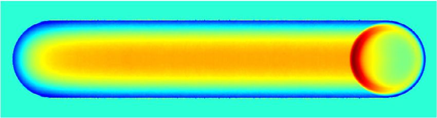
COMMUNICATIONS PHYSICS | https://doi.org/10.1038/s42005-021-00632-1 ARTICLE
a 0.9 Molten zone b 0.8
1 mm s-1 100 mm s-1
0.8 Steady-state region 10 mm s-1 200 mm s-1
Ge molar fraction x (mol)
Ge molar fraction x (mol)
0.7
50 mm s 500 mm s-1
0.7
0.6
0.6
0.5 0.5
0.4 -1 -1
Initial Ge
1 mm s 100 mm s
0.4 content
0.3 10 mm s-1 200 mm s-1
50 mm s 500 mm s-1 0.3
0.2
0 2 4 6 8 10 -1.5 -1 -0.5 0 0.5 1 1.5
Longitudinal position on the top surface (µm) Transverse position on the top surface (µm)
c 0.8 d 1
1 mm s-1 100 mm s-1 1 mm s-1 100 mm s-1
10 mm s-1 200 mm s-1 10 mm s-1 200 mm s-1
Ge molar fraction x (mol)
0.7
0.8
50 mm s 500 mm s-1 50 mm s 500 mm s-1
Volume distribution
0.6
0.6
0.5
0.4
0.4 Initial Ge
content
0.2 Solidified
0.3
volume
Depth of the melt region
0.2 0
0 0.1 0.2 0.3 0.4 0.5 0 0.2 0.4 0.6 0.8 1
Vertical position along the cross-section (µm) Ge molar fraction x (mol)
Fig. 3 Simulation results showing the Si1−xGex composition profiles along different directions on various surfaces, and dispersion of the composition
for scan speeds in the range of 1–500 mm s−1. Inset figures show the surface and direction (dotted lines) where the composition profile was taken. Ge
molar fraction x(r) along the a longitudinal and b transverse directions on the top surface, and c along the vertical direction at the cross-sections of laser-
written SiGe microstripes. d Normalized volume histogram showing the scan-speed-dependent dispersion of the initial composition x0 = 0.5 within the
whole solidified volume in terms of the Ge molar fraction. The bin size for histograms is Δx = 0.01. Inset figure shows the laser-processed volume in the
steady-state region, where the histograms were calculated.
90
a HAADF d
(Depth) Initial Ge profile (EDX)
80
Ge profile after
laser processing (EDX)
SiGe 70
Phase-field simulation
Si substrate 1 µm
Germanium content (%)
60
b EDX
50
40
1 µm 30
c Phase-field simulation 20
Si
SiGe epilayer wafer
10
0
Si Ge 0 0.1 0.2 0.3 0.4 0.5 0.6 0.7 0.8
0 0.2 0.4 0.6 0.8 1
Si1-xGex Depth (µm)
Fig. 4 Elemental analysis of an in-plane longitudinal SiGe heterostructure laser-written at a scan speed of 200 mm s−1. a High-angle annular dark-field
image (HAADF) showing the material contrast at the cross-section of the laser-processed region. b Energy-dispersive X-ray spectroscopy (EDX) and c
phase-field simulation results showing spatial redistribution of the alloy composition at the cross-section for 2D comparison. The color scale applies to
both figures in b, c. d Quantitative comparison between the experimental (blue solid line) and simulated (red dashed line) Ge concentration along the
depth profile across the cross-section, as marked by a white arrow in a. The experimental error margin in the EDX data is 5%.
COMMUNICATIONS PHYSICS | (2021)4:132 | https://doi.org/10.1038/s42005-021-00632-1 | www.nature.com/commsphys 5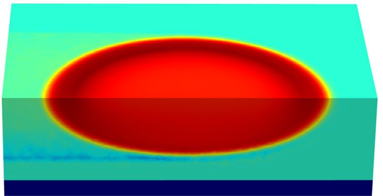
ARTICLE                                                                    COMMUNICATIONS PHYSICS | https://doi.org/10.1038/s42005-021-00632-1

              a              Si1-xGex (mol)             c      Simulated TE mode profile            e              TE mode profile
                                                        0                   Emax
                    0   0.1 0.2 0.3 0.4 0.5 0.6 0.7
                                                                (a.u.)

                                                                                             1 µm

              b          Refractive index profile       d      Simulated TM mode profile             f            TM mode profile
                                                        0                   Emax
                         1 1.5 2 2.5 3 3.5      4               (a.u.)
              Air

              SiGe

                                               0.5 µm                                        1 µm
              Si

Fig. 5 Laser-written in-plane longitudinal SiGe heterostructures as graded-index optical waveguides. a Simulated spatial redistribution of Ge molar
fraction x(r) and b calculated refractive index n(x) of the cross-section of a SiGe heterostructure laser-written at a scan speed of 200 mm s−1. Simulated c
transverse electric (TE) and d transverse magnetic (TM) polarized mode profiles obtained by modal analysis using the refractive index profile n(r) in b.
Infrared (IR) camera image showing the experimentally captured intensity profiles for the e TE and f TM polarized modes of light, which was free space
coupled into the 1 cm long laser-written SiGe waveguides using a fiber laser emitting at 2 µm.

of ±5%. It is worth noting that even in the case of laser processing               waveguide by using a 60× objective. The light at the output was
at a scan speed of 200 mm s−1, where the maximum composi-                          then collimated by a 40× objective and imaged by an infrared
tional segregation occurs, the Ge concentration profile is                          camera to capture the images of the TE and TM modes shown in
smoothly changing across the cross-section, as can be seen in                      Fig. 5e, f, respectively. A schematic for the experimental setup
Fig. 4d. However, an abrupt transition occurs within a 25 nm                       used for optical coupling is given in Supplementary Fig. 4. In
range at the melt/solid boundary, jumping from the lowest Ge                       agreement with the optical simulations, we observed that only the
content (25%) to the initial Ge content (50%) of the SiGe epilayer.                fundamental TE and TM modes were guided through these laser-
                                                                                   written SiGe waveguides at a wavelength of 2 µm. Moreover,
                                                                                   optical guiding was observed even for the waveguide written at
Modal analysis of in-plane longitudinal SiGe heterostructures                      the lowest scan speed of 0.1 mm s−1, where the least composi-
that function as laser-written graded-index waveguides. Similar                    tional segregation occurs within the laser-processed region. This
to the double heterostructure semiconductor lasers, where optical                  observation confirms our assumption that the residual tensile
guiding is achieved in a high-index core sandwiched between two                    strains increase the refractive index in the laser-processed regions
lower index claddings, a single longitudinal heterostructure                       to allow for optical guiding. The TM mode was found to be lossy;
formed with a Ge-rich stripe core and a surrounding Si-rich                        therefore, it leaks from the strip core decreasing the intensity of
cladding can provide confinement for light. To illustrate this                      the propagating light. More confinement is necessary for the TM
concept, we calculated the optical modes supported by a long-                      mode to achieve optical guiding at much longer wavelengths,
itudinal heterostructure laser-written at a scan speed of 200 mm s−1               such as in the molecular fingerprint regime (6–20 µm wave-
by a focused beam of 2 µm in diameter. The 2D Ge molar fraction                    length). The depth of the melted region is naturally limited by the
at the cross-section of the laser-written SiGe microstripe, which was              thickness of the SiGe epilayer, which can be grown on a Si
obtained by a phase-field simulation, is given in Fig. 5a. The cor-                 substrate with a thickness up to 10 µm using CVD methods. By
responding refractive index profile n(x) at a wavelength of 2 µm was                increasing the laser power and using longer wavelengths (>532
calculated by using n(x) = 3.451 + 0.2951x + 0.3419x2, which is a                  nm), the deposited energy and optical penetration can be
quadratic function of the Ge molar fraction38.                                     increased to deepen the melted region closer to the SiGe/Si
   The process temperatures, which are high enough to melt the                     interface.
surface, result in biaxial tensile strains within the laser-processed                 Conventional waveguides depend on patterning of silicon-on-
SiGe films, due to the difference between the thermal expansion                     insulator (SOI) wafers by e-beam lithography and etching.
coefficients of Ge and Si. Residual tensile strains as high as 0.6%                 Although this approach provides compact components for
can be reached28. Therefore, photo-elastic effects, which are                      integrated photonics in the telecom range, the silica buffer oxide
strain-induced changes in the refractive index n, need to be                       layer in SOI waveguides suffers from strong absorption above 3.6
incorporated39. We found that an increase of 3% in the refractive                  μm, hindering photonic applications in the mid-IR range.
index within the laser-processed strained region gives the best                    Therefore, graded-index SiGe waveguides have recently received
agreement with the optical experiments in terms of matching the                    increased interest for mid-IR applications in integrated
mode profiles. The resulting refractive index profile, which                         photonics40,41, due both to the low optical losses (1–2 dB cm−1)
includes the photo-elastic effects, is shown in Fig. 5b. The                       in the wavelength range of 2–8 µm and their tunable optical
simulated fundamental mode profiles for the transverse electric                     properties via compositional engineering. However, these graded-
(TE) and transverse magnetic (TM) polarized light at a                             index SiGe waveguides fabricated by epitaxial growth have two
wavelength of 2 µm are shown in Fig. 5c, d, respectively.                          drawbacks: i) The graded refractive index can only be obtained in
   For a proof-of-principle demonstration, we used a 1 cm long                     the growth direction perpendicular to the substrate surface, and a
SiGe microstripe that was written using a laser with a spot size of                step index profile in the plane for mode confinement still requires
5 µm at a scan speed of 200 mm s−1. The end facets were                            patterning of the surface similar to the SOI waveguides. ii)
prepared for optical coupling by manual cleaving, and a 2 µm                       Waveguides with different graded index profiles on the same
fiber laser was first free space coupled into the graded-index SiGe

6                             COMMUNICATIONS PHYSICS | (2021)4:132 | https://doi.org/10.1038/s42005-021-00632-1 | www.nature.com/commsphys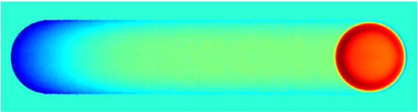
COMMUNICATIONS PHYSICS | https://doi.org/10.1038/s42005-021-00632-1                                                                ARTICLE

substrate require different growth processes for each of them,                 higher acceleration of the solidification boundary when the spot
increasing the cost and complexity of the fabrication. In contrast,            size suddenly shrinks. Another approach for modulation is
for the laser-written graded-index SiGe waveguides, an index                   switching the position of the focused laser beam back and forth in
grading both in the transverse and vertical directions at the cross-           the scan direction while the stage moves at a constant scan speed.
section is simultaneously achieved via compositional segregation               A 61.1 kHz sawtooth modulation of the beam position with a
of the alloy within the melt region during laser processing.                   movement of 200 nm resulted in a SiGe superlattice with a period
Moreover, this graded index profile is tunable by controlling the               of Λ = 410 nm (see Fig. 6d). Slowing the speed of the laser beam
laser scan speed, allowing fabrication of customized waveguides                in the return cycle helps to lower the Ge molar fraction (down to
using the same homogeneous SiGe epilayer grown on a Si                         x0 = 0.5) between the two maxima of the composition. Periodic
substrate. A tunable index profile can be leveraged for dispersion              heterostructure formation via modulation of the beam position
engineering in nonlinear optical applications. Furthermore,                    and power are shown in Supplementary Movies 1 and 2,
compositional segregation of Si and Ge enables a refractive index              respectively.
difference Δn on the order of 10−1, which is higher compared to
those typically obtained (10−4) in laser-written waveguides in
                                                                               Optical simulations for transmission and reflection spectra of
bulk      unary     semiconductors     via    pulsed-laser-induced
                                                                               waveguide Bragg gratings based on in-plane transverse SiGe
modifications42. Furthermore, laser writing of SiGe waveguides
                                                                               superlattices. Waveguide Bragg gratings, which consist of alter-
does not require lithographic patterning, which can lead to
                                                                               nating layers with different refractive indices, is one of the basic
scattering losses due to the roughness of the etched waveguide
                                                                               elements used in integrated photonics today. Primary methods
boundaries, and it can be used to write components with complex
                                                                               used to fabricate Bragg gratings are material removal by
shapes such as directional couplers, Y-junctions, S-bends, and
                                                                               etching44, and local refractive index modification induced by
spirals, if 2-axis motorized stages are used43.
                                                                               ultra-fast lasers45. Laser-written in-plane transverse SiGe super-
                                                                               lattices can be exploited as a waveguide Bragg grating if the period
                                                                               Λ of the grating satisfies the first-order Bragg condition λ = 2neff
Phase-field simulations of in-plane periodic transverse het-
                                                                               Λ, where λ is the wavelength of interest, and neff is the effective
erostructures (superlattices) fabricated by modulation of the
                                                                               index of the reflected optical mode.
laser processing parameters. As the steady-state region within
                                                                                  We simulated an in-plane transverse SiGe superlattice laser-
the laser-written microstripes is indefinitely long (depending only
                                                                               written at a constant stage scan speed of 25 mm s−1, using a
on the total scan range), the laser processing parameters can be
                                                                               sawtooth modulation of the laser beam position with a movement
modulated to create transient effects superimposed on the con-
                                                                               of 200 nm (see Fig. 7a). A 10-period Bragg grating with a period
stant scan speed of the stage during laser processing. To inves-
                                                                               of Λ0 = 285 nm was chosen for a filtering application at a
tigate the idea, we first performed simulations with the
                                                                               wavelength range around 2 µm. The total length of the Bragg
modulation of the stage scan speed to produce periodic hetero-
                                                                               grating was kept short, due to the computational constraints of
structures in the steady-state region (see Fig. 1b). A 77.6 kHz
                                                                               the FEM-based optical simulations in 3D. However, to increase
square wave modulation of the stage scan speed v between 25–50
                                                                               the coupling between propagating and counter-propagating
mm s−1 with a duty cycle of 1/3 resulted in a SiGe superlattice
                                                                               modes in such a short waveguide Bragg grating, we ensured that
with a period of Λ = 430 nm (see Fig. 6a). The resulting periodic
                                                                               the maximum refractive index modulation was achieved in the
composition profile is embedded into the Ge-rich strip core and
                                                                               periodic composition profile (Δx = 0.45–0.75 mol), as shown in
diminishes close to the surrounding Si-rich cladding (down to a
                                                                               Fig. 7b. The calculated transmission and reflection spectra of the
depth of 300 nm), as shown in the inset figure. The composition
                                                                               10-period waveguide Bragg grating are shown in Fig. 7c. Further
profile (blue) along the longitudinal direction on the top surface
                                                                               details regarding implementation of the optical simulations are
shows the profile of the Ge molar fraction, where the stationary
                                                                               given in Supplementary Note 2.
background composition level is determined by the initial scan
                                                                                  A dip in the transmission spectrum was observed at a
speed (see Fig. 3a). It is possible to obtain a higher background
                                                                               wavelength of 2038.9 nm for the reflected TE mode with an
composition level up to the maximum Ge molar fraction of x =
                                                                               effective index of neff = 3.5244. By using the Bragg condition, we
0.7 by increasing the initial scan speed; however, this requires
                                                                               found that this corresponds to a period Λ of 289.3 nm, which is
application of higher modulation frequencies to achieve the same
                                                                               close to the simulated period Λ0 = 285 nm. A slight mismatch is
period. To demonstrate a smaller period and a different back-
                                                                               expected due to the coarser size of the mesh (40 nm) used for the
ground composition level, we performed a 621.1 kHz modulation
                                                                               optical simulations. Additionally, we noticed that the reflection
of the stage scan speed v between 100–200 mm s−1, which forms
                                                                               was suppressed, which is desired for a notch filter application.
a SiGe superlattice with a period of Λ = 220 nm, as shown in
                                                                               The reduction in the reflection is common for single mode
Fig. 6b. Although smaller periods down to 100 nm could be
                                                                               waveguides with asymmetric gratings, like a tilted fiber Bragg
achieved, the finiteness of the mesh (minimum 20 nm) limits the
                                                                               grating, which couple the reflected light into higher order lossy
resolution of the simulated heterostructures.
                                                                               modes. As our graded-index SiGe waveguides support only the
   Modulation of the scan speed by controlling the movement of
                                                                               fundamental TE mode at a wavelength of 2000 nm, we expect
the stage, where the SiGe sample is fixed, might be experimentally
                                                                               high losses for the reflected higher order modes. A waveguide
limited by the maximum achievable acceleration due to the
                                                                               Bragg grating with a high number of periods (>1000) and a longer
inertia of the stage mechanism. Much faster motional transients
                                                                               total length (>300 µm) would be straightforward to fabricate to
for the laser-induced molten zone can be realized by modulating
                                                                               achieve better rejection ratios in the stop band, and thus could
either power or position of the laser beam using electro-optic
                                                                               find ready use in integrated photonics applications.
modulators/deflectors or acousto-optic scanners, while the stage
moves independently at a constant scan speed. We performed
20% modulation (reduction) of the laser power P0 = 200 mW                      Discussion
with a duty cycle of 1/3 at 61.0 kHz to obtain an in-plane                     Laser-driven phase segregation in homogeneous Si0.5Ge0.5 epi-
transverse SiGe superlattice with a period of Λ = 402 nm (see                  layers allows for achieving Ge concentrations remarkably higher
Fig. 6c). In this case, we were able to obtain a greater change in             (x > 0.7) and lower (x < 0.25) than the initial concentration within
the Ge molar fraction in the range of Δx = 0.55–0.78 mol, via the              the strip core and under-cladding, respectively. To obtain higher

COMMUNICATIONS PHYSICS | (2021)4:132 | https://doi.org/10.1038/s42005-021-00632-1 | www.nature.com/commsphys                                     7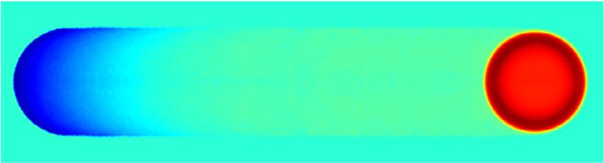
ARTICLE COMMUNICATIONS PHYSICS | https://doi.org/10.1038/s42005-021-00632-1
a Laser scan direction b
A B
P0 = 0.2 W v0 = 25 mms-1 P0 = 0.2 W v1 = 100 mms-1
0.9
Modulation of scan speed v0 Modulation of scan speed v1 Ge
Si1-xGex (mol)
Ge molar fraction x (mol)
0.8 0.8
0.7
Λ 0.6
0.7 0.5
0.4
0.6 A B 0.3
Si
0.5
2×V0 2×V1
0.4
V0 V1
0.3
0 0.05 0.1 0.15 (ms) 0 0.01 0.02 0.03 0.04 (ms)
0.2
0 1 2 3 4 5 6 7 8 9 10 0 1 2 3 4 5 6 7 8 9 10
Longitudunal position on the top surface (µm) Longitudunal position on the top surface (µm)
c d 0 D0
P0 = 0.2 W v0 = 25 mms-1 D0 = 200 nm v0 = 25 mms-1
0.9
Modulation of optical power P0 Modulation of beam position D0
Ge molar fraction x (mol)
0.8
0.7
0.6
0.5
0 0.05 0.1 0.15 0.2 (ms) D0
0.4 P0
0.3 0
0.8×P0
0 0.05 0.1 0.15 0.2 (ms)
0.2
0 1 2 3 4 5 6 7 8 9 10 0 1 2 3 4 5 6 7 8 9 10
Longitudunal position on the top surface (µm) Longitudunal position on the top surface (µm)
Fig. 6 Laser-written in-plane transverse SiGe superlattices fabricated by sub-millisecond modulation of the scan speed, optical power, and beam
position. Composition color maps show the Ge molar fraction x on the top surface of the laser-written microstripes. Inset figures show the periodic
composition distributions at the transverse and longitudinal cross-sections to reveal the depth of the modulated regions. Modulated laser processing
parameters and resulting composition profiles on the top surface are given in red and blue colors, respectively. All square wave modulations have a duty
cycle of 1/3. a A 77.6 kHz square wave modulation of the stage scan speed v between 25–50 mm s−1 results in an in-plane SiGe superlattice with a period
of Λ = 430 nm. b 621.1 kHz modulation of the stage scan speed v between 100–200 mm s−1 forms a SiGe superlattice with a period of Λ = 220 nm. c
While the stage moves at a constant speed of 25 mm s−1, 61.0 kHz 20% modulation (reduction) of the laser power P0 = 0.2 W forms a SiGe superlattice
with a period of Λ = 402 nm. d 61.1 kHz sawtooth wave modulation of the beam position with a back-and-forth movement of 200 nm forms a SiGe
superlattice with a period of Λ = 410 nm. The color scale applies to all composition maps.
Ge concentrations, SiGe epilayers with an initially higher Ge To further control the transverse patterning, laser beam sha-
content can be used. According to our phase-field simulations, pers can be used to obtain non-circular beam shapes. For
laser processing of a SiGe epilayer with an initial 80% Ge content example, in-plane traverse heterostructures with straight inter-
at a scan speed of 200 mm s−1 enables a 95% Ge content to be faces perpendicular to the scan direction, required for quantum
reached at the top surface of the strip core. The initial Ge content well-like structures, could be written using a rectangular-shaped
can be further increased, however, the strength of the phase laser beam. Although the transverse size of the periodic hetero-
segregation decreases due to narrowing of the gap between the structures is determined by the diameter of the focused laser spot,
liquid and solidus curves in the phase diagram. In contrast, using the spatial period is not diffraction-limited. This is because it is
transient effects such as the acceleration of the liquid/solid not the spot area47, but the displacement of the 2D liquid/solid
boundary via modulation of the laser processing parameters has a interface in the scan direction that determines the period, which
stronger effect in terms of reaching a higher Ge content. This in principle can be as small as the modulation frequency of the
could potentially lead to the fabrication of in-plane transverse laser processing parameters can be increased. Thus, the width of
heterostructures having pure Ge in Ge-rich SiGe epilayers, which the quantum wells that could be written into the epilayers is
are in high demand for development of spin-based quantum determined by multiplication of the constant scan speed and
technologies46, as well as for fabrication of quantum wells and modulation period Δt. For example, to fabricate a quantum well
superlattices, which could be used as building blocks of photonic with a width of 20 nm, the modulation period should be 1 µs for a
and optoelectronic devices including photodetectors and scan speed of 20 mm s−1. This corresponds to a modulation
modulators. frequency of 1 MHz, which is within the capabilities of state-of-
8 COMMUNICATIONS PHYSICS | (2021)4:132 | https://doi.org/10.1038/s42005-021-00632-1 | www.nature.com/commsphys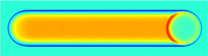
COMMUNICATIONS PHYSICS | https://doi.org/10.1038/s42005-021-00632-1 ARTICLE
a Ge b 0.85 c 1
10 period Bragg grating
0.8 0.9
0.8 Λ = 285 nm
Ge molar fraction x (mol)
Si1-xGex (mol)
0.7 0.8
Optical power (a.u.)
0.6 0.75
0.7
0.5 0.7 0.6 Transmission
0.4 0.65 0.5
0.3
0.6 0.4
Si Reflection (×10)
0.55 0.3
0.5 0.2
0.45 0.1
0
TE
0 0.5 1 1.5 2 2.5 3 3.5 4 2034 2036 2038 2040 2042 2044
Transmitted intensity profile Longitudinal position on the top surface (µm) Wavelength (nm)
Fig. 7 Laser-written in-plane transverse SiGe superlattice on a silicon substrate as a waveguide Bragg grating. a Composition color map shows the
periodic Ge molar fraction x on the top surface of an in-plane transverse SiGe superlattice written at a constant stage scan speed of 25 mm s−1, using a
sawtooth wave modulation of the laser beam position (back and forth movement of 200 nm) in the scan direction. Calculated optical intensity profile of a
transverse electric (TE) polarized mode is shown as superimposed on the output facet of the simulated waveguide Bragg grating. b Ge molar fraction
profile as a function of position along the center line on the top surface showing a 10-period grating with a period of 285 nm. c Calculated transmission and
reflection spectra of the 10-period SiGe waveguide Bragg grating by using finite-element-method (FEM)-based optical simulations. The reflection data (red
bottom line) is magnified ten times for clarity.
the-art electro-optic laser beam modulators and deflectors. volume and a constant pressure for a regular solution model of binary alloys by48,
However, the estimated average thickness of the mushy solid/
F ϕ; T; x ¼ E ϕ; T; x TS E ϕ; T; x ; ϕ; x ;
liquid interface is 90 nm, which depends on the local thermal
¼ ð1 xÞFSi ϕ; T þ xFGe ϕ; T ð1Þ
gradients, and mushy zone range at x0 = 0.5. Therefore, we
þ RT ½ð1 xÞ lnð1 xÞ þ xlnðxÞ þ w ϕ xð1 xÞ;
expect that the width of the quantum wells could be decreased
further by setting the spatial period of the modulation smaller where E(ϕ, T, x) is the total internal energy, S(E(ϕ, T, x), ϕ, x) is the total entropy, T
than 90 nm. However, this would compromise the modulation is the temperature, x is the molar fraction of Ge, R is the ideal gas constant, ϕ is the
phase-field representing the solid (ϕ = 0) and liquid (ϕ = 1) phases. FSi (ϕ, T) and
depth Δx in composition, which is the maximum compositional FGe (ϕ, T) are the Gibbs free energies in units of J mol−1 for pure Si and Ge,
difference between the well and barrier regions. It is worthnoting respectively. The molar Gibbs free energy for a pure element A (Si or Ge) is given
that these laser-written in-plane transverse heterostructures do by49,
not have an atomically-sharp interface, but a gradual one, which
T
could be useful to fabricate graded confining potentials36. FA ϕ; T ¼ EA ϕ; T TSA ϕ; T ¼ HA g ϕ þ LA 1 A p ϕ þ FA;Solid ;
Tm
For the fabrication of active devices based on in-plane het- ð2Þ
erostructures, a doping process is required. Conventionally,
where EA (ϕ, T) and SA(ϕ, T) are the internal energy and entropy for the pure
doping can be realized after laser processing by either ion- element A, respectively; HA is the height of the energy barrier between the liquid
implantation or thermally assisted diffusion from a dopant and solid phases at the melting temperature Tm A
; LA is the latent heat of melting; g
source. However, this would compromise the crystalline structure (ϕ) = ϕ2 (1 − ϕ)2 is the double-well potential function with minima at ϕ = 0 and ϕ
and Ge profile of the superlattices, decreasing the compositional = 1; and p(ϕ) = ϕ2 (3 − 2ϕ) is an interpolating function, which satisfies p(ϕ = 0) =
contrast between the well and barrier regions. SiGe epilayers can 0 and p(ϕ = 1) = 1. The height of the energy barrier HA is assumed to be the same
for Si and Ge, due to the similar atomic properties. FA,Solid is the Gibbs free energy
also be doped during epitaxial growth via CVD. Laser post- of the solid pure element A, which is assumed to be zero. The last term in Eq. (1) is
processing can be then applied to these initially doped SiGe the molar excess Gibbs free energy, which is proportional to the parameter w(ϕ)
epilayers to fabricate in-plane doped heterostructures. The most given by
appealing aspect of this strategy would be simultaneous activation
w ϕ ¼ wS 1 ϕ þ wL ϕ; ð3Þ
of the dopants without requiring an additional annealing process,
though it could also result in a redistribution of the dopants where wS and wL are regular solution parameters corresponding to solid and liquid
phases of the SiGe alloy, respectively.
within the heterostructures. Another useful avenue to explore The chemical potentials µ for Si and Ge can be calculated from the molar Gibbs
would be to populate un-doped Ge-rich heterostructures with energy F(ϕ, T, x) in Eq. (1) as:50
charge carriers by either using modulation doping or gate- ∂F
induced accumulation from the ohmic contacts46. Finally, laser- μSi ðϕ; T; xÞ ¼ F x ¼ w ϕ x2 þ FSi ϕ; T þ RT lnð1 xÞ; ð4Þ
∂x
driven phase segregation with modulation of the laser process
parameters could also be applied to fabricate in-plane hetero- ∂F
μGe ðϕ; T; xÞ ¼ F þ ð1 xÞ ¼ w ϕ ð1 xÞ2 þFGe ϕ; T þ RTlnðxÞ: ð5Þ
structures in other pseudo-binary systems, such as metal alloys ∂x
(Ni–Cu), ternary semiconductor alloys (AlxGa1−xAs), quaternary In the case of phase coexistence at thermal equilibrium, the chemical potential
alloys of transition metal dichalcogenides (MoxW1−xSySe1−y)14, for each element in the solid (S) and liquid (L) solutions are equal, and given by
and ceramics (Al2O3–Cr2O3), which have phase diagrams similar μSSi ϕ ¼ 0; T; xS ¼ μLSi ϕ ¼ 1; T; xL ; ð6Þ
to that of SiGe alloy.
μSGe ϕ ¼ 0; T; xS ¼ μLGe ϕ ¼ 1; T; xL ; ð7Þ
where xS and xL are the Ge molar fractions in the solid and liquid solutions of Si1
Methods −xGex, respectively. By using Eqs. (2–7) can be rewritten explicitly in terms of the
Calculation of the equilibrium phase diagram for SiGe alloys. We used the regular solution parameters, latent heats of melting, and melting temperatures of
molar Gibbs free energy F to calculate the equilibrium phase diagram of SiGe the alloy elements50, as given below
alloys. By fitting it to the experimental phase diagram data, we estimated the
parameters in the molar Gibbs free energy F(ϕ,T, x), which is given at a constant 1 xS LSi 1 1 1
ln ¼ Si þ w x2 wS xS2 ; ð8Þ
1 xL R T Tm RT L L
COMMUNICATIONS PHYSICS | (2021)4:132 | https://doi.org/10.1038/s42005-021-00632-1 | www.nature.com/commsphys 9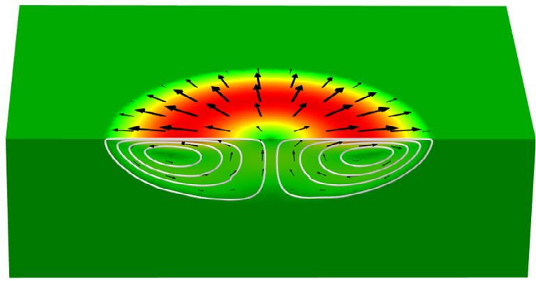
ARTICLE COMMUNICATIONS PHYSICS | https://doi.org/10.1038/s42005-021-00632-1
xS LGe 1 1 1 ∂ϕ ∂s 1 ∂f
ln ¼ Ge þ w ð1 xL Þ2 wS ð1 xS Þ2 ; ð9Þ ¼ Mϕ þ ε2ϕ ∇2 ϕ ¼ Mϕ ε2ϕ ∇2 ϕ ; ð18Þ
xL R T Tm RT L ∂t ∂e T ∂ϕ
which are implicit analytic expressions for the liquidus xL(T) and solidus xS(T) where Me, Mx, and Mϕ are positive-definite parameters, and T(r,t) is the
curves in the phase diagram of SiGe. As shown in Supplementary Fig. 1, the best temperature field. In the kinetic equations in Eqs. (16–18), the partial derivatives of
fitting parameters (normalized by the ideal gas constant R) for the experimental the entropy density s are rewritten in terms of the partial derivatives of the free
phase diagram were found to be Tm Si
= 1687 K, LSi/R = 6040 K, TmGe
= 1211 K, LGe/ energy density f(ϕ, T, x), which is in units of J m−3 and derived from the molar
R = 4441 K, wS/R = 450 K and wL/R = 800 K. Gibbs free energy F given in Eq. (1), divided by the molar volume Vm of the SiGe
alloy:
Thermocapillary-driven convection in the laser-induced molten zone. Fðϕ; T; xÞ
f ϕ; T; x ¼ ; ð19Þ
Buoyancy-driven convection within the laser-induced melt pool was neglected Vm
because the highest temperature is reached on the top surface, where the fluid with By adding a conservative convection term ∇ · (u x) on the left-hand side of Eq.
the lowest density already resides. In contrast, the thermocapillary effect (Mar- (16), a segregation-diffusion-convection equation is finally derived as,
angoni effect), which is due to the temperature-dependent surface tension σ(T), is
the dominant driving force for the convection, which can result in fluid flows with ∂x ∂ 1 ∂f ∂ 1 ∂f ∂ 1 ∂f
þ ∇ ðuxÞ ¼ ∇ Mx ∇x þ ∇ϕ þ ∇T :
maximum speeds umax in a range of 1–10 m s−1 for semiconductors melted by ∂t ∂x T ∂x ∂ϕ T ∂x ∂T T ∂x
lasers51,52. The laser-processed SiGe films were treated as a highly viscous liquid ð20Þ
with a dynamic viscosity μ(ϕ) varying by several orders of magnitude between the
solid phase (µS = 1.0 × 10³ N s m−2) and liquid phase (µL = 0.8 × 10⁻³ N s m−2), Here, ∂f/∂x is calculated from Eqs. (1, 19) as
which is given in the form ∂f 1 T T x
¼ LGe 1 Ge LSi 1 Si p ϕ þ RTln þ w ϕ ð1 2xÞ :
μ ϕ ¼ μL p ϕ þ μS 1 p ϕ ; ð10Þ ∂x Vm Tm Tm 1x
ð21Þ
where p(ϕ) is the interpolation function. The surface tension σ for the liquid SiGe
To ensure a composition independent diffusion coefficient D, the mobility Mx is
alloy, which was estimated using the surface tensions of liquid Si and Ge53, is
taken as
assumed to be a linear function of temperature T as
DðϕÞT V D ϕ T ð1 xÞx
σ ðT Þ ¼ 0:653 N m1 104 N m1 K 1 T Tm ; ð11Þ Mx ¼ 2 2 ¼ m ; ð22Þ
∂ f ϕ; T; x =∂ x RT 2xð1 xÞw ϕ
where Tm is the melting temperature of the alloy.
To describe fluid motion in the molten pool due to the thermocapillary where the phase-dependent diffusion coefficient is
convection, we solved Navier–Stokes equations, which in a general form read as
D ϕ ¼ DS 1 ϕ þ DL ϕ: ð23Þ
∇ ρu ¼ 0; ð12Þ The diffusion coefficients in the liquid and solid SiGe phases are taken as DL =
3.0 × 10⁻⁸ m2 s−1 and DS = 10−16 m2 s−1, respectively. When ∇ϕ = 0 and ∇T =
∂u 0, the standard diffusion equation is obtained, as the Ge concentration C is related
ρ þ ρðu ∇Þu ¼ ∇ pI þ μ ∇u þ ∇uT þ F; ð13Þ to the Ge molar fraction x by C = x/Vm.
∂t
By using Eqs. (1, 2, and 19), the energy density of a partially-melted alloy can be
where ρ is the fluid density, u is the velocity field, p is the dynamic pressure, I is the written as48,
unity tensor, and F is a source term representing body sources, such as gravity
force. We also assumed a laminar incompressible flow (∇∙u = 0) for the e x; ϕ; T ¼ ð1 xÞeSi ϕ ; T þ xeGe ϕ; T þ w ϕ xð1 xÞ; ð24Þ
simulations. The thermocapillary effect is a shear stress, which depends on the where eSi and eGe are energy densities of pure Si and Ge. For a pure element A (Si
tangential temperature gradient, and it was implemented as a surface boundary or Ge), we assume that eA can be written as,
condition
eA ϕ; T ¼ eA;S ðT Þ 1 ϕ þ eA;L ðT Þϕ; ð25Þ
pI þ μ ∇u þ ∇uT n ¼ γ½∇T nðn ∇T Þ; ð14Þ
where eA,S and eA,L are the energy densities of the solid and liquid phases of the
where n is the vector normal to the fluid surface, and γ = dσ/dT is the temperature pure element. By inserting Eqs. (3, 25) into Eq. (24), the energy density of the alloy
derivative of the surface tension σ in Eq. (11). can be rewritten as
h i
Non-isothermal phase-field formulation of the segregation-diffusion- e x; ϕ; T ¼ ð1 xÞeSi;S ðT Þ þ xeGe;S ðT Þ þ wS ð1 xÞx 1 ϕ ;
convection equation and heat transport equation. To describe the laser melting h i ð26Þ
process, a segregation-diffusion-convection equation needs to be formulated þ ð1 xÞeSi;L ðT Þ þ xeGe;L ðT Þ þ wL ð1 xÞx ϕ:
incorporating phase segregation in the laser-melted SiGe epilayers, as well as the The terms in the square brackets in Eq. (26) are defined as hS and hL for the
convection in the molten pool, which is driven mainly by the thermocapillary solid and liquid phases of the alloy, respectively, to obtain a compact form for the
effect. For a thermodynamically consistent derivation of a non-isothermal phase- energy density, which is rewritten as:
field model54, we postulate an entropy functional ^S defined by the integral of the
entropy density s(e,ϕ, x) over the whole SiGe epilayer volume, as given by e x; ϕ; T ¼ hS ðx; T Þ 1 ϕ þ hL ðx; T Þϕ: ð27Þ
Z " # These terms depend on the composition and temperature, as implied by Eq.
ε2e 2 εx
2 ε2ϕ 2 (26). The composition is determined by the initial Ge fraction x0 of the initially-
^S ¼ s e; ϕ; x j∇ej j∇xj ∇ϕ dV;
2 ð15Þ
2 2 2 homogeneous alloy. To simplify the implementation of the simulations, we assume
the x-dependent terms in hS and hL stay constant in the following derivation.
where e is the energy density, ϕ(r, t) is the phase-field parameter representing the Furthermore, the density ρ of the SiGe alloy is also assumed to be constant
solid domains and traveling molten zone in the Si1−xGex epilayer. The gradient (temperature independent) and the same for both phases.
coefficient εx is generally required at very high scan speeds (>1 m s−1), where the For derivation of a heat transport equation55, by inserting Eq. (27) into Eq. (17),
characteristic length Ls of the solute boundary layer approaches atomic dimensions we obtain
and solidification occurs without redistribution of the composition (partitionless
solidification). However, Ls is 60 nm for our maximum scan speed of 0.5 m s−1, 1 dhS 1 dhL dT h hS dϕ dT M
ρ 1ϕ þ ϕ þρ L ¼ ∇ 2e ∇T; ð28Þ
thus εx could be neglected. εe was also neglected as it is not part of the conventional ρ dT ρ dT dt ρ dT dt T
heat transport equation, which will be derived in the following paragraphs. εϕ,
where the density of the alloy is inserted to convert the energy density to energy per
which is related to the thickness and energy of the solid/liquid interface, was
mass. Equation (28) can then be recast into the conventional heat transport
assumed to be constant.
equation as
Time-dependent equations, which ensure positive local entropy production
according to the laws of thermodynamics48, can be derived for the Ge molar dϕ dT
fraction, energy density, and phase-field parameter as ρ cp;s 1 ϕ þ cp;l ϕ þ L ¼ ∇ k∇T: ð29Þ
dT dt
∂x ∂s 1 ∂f Here, k = Me/T2 is the thermal conductivity, and cp,s and cp,l are the specific heat
¼ ∇ Mx ∇ ¼ ∇ Mx ∇ ; ð16Þ
∂t ∂x T ∂x capacity of the solid and liquid phases, respectively. The terms in the square
parenthesis can be defined as an apparent heat capacity cp
∂e ∂s 1 dϕ
¼ ∇ Me ∇ ¼ ∇ Me ∇ ; ð17Þ cp ¼ cp;s 1 ϕ þ cp;l ϕ þ L ; ð30Þ
∂t ∂e T dT
10 COMMUNICATIONS PHYSICS | (2021)4:132 | https://doi.org/10.1038/s42005-021-00632-1 | www.nature.com/commsphysYou can also read