THE TRANSPORT PROPERTIES OF ULTRATHIN 2H-NBSE2 - HPSTAR
←
→
Page content transcription
If your browser does not render page correctly, please read the page content below
Superconductor Science and Technology
Supercond. Sci. Technol. 34 (2021) 025019 (5pp) https://doi.org/10.1088/1361-6668/abd14f
The transport properties of ultrathin
2H–NbSe2 HPSTAR
1107-2021
L B Lei1,2,3, C Zhang2,3,4, A B Yu2,3,4, Y F Wu5, W Peng2,3,4, H Xiao6, S Qiao1,2,3,4
and T Hu5
1
ShanghaiTech University, Shanghai 201210, People’s Republic of China
2
State Key Laboratory of Functional Materials for Informatics, Shanghai Institute of Microsystem and
Information Technology, Chinese Academy of Sciences, Shanghai 200050, People’s Republic of China
3
CAS Center for Excellence in Superconducting Electronics (CENSE), Shanghai 200050,
People’s Republic of China
4
University of Chinese Academy of Sciences, Beijing 100049, People’s Republic of China
5
Beijing Academy of Quantum Information Sciences, Beijing 100193, People’s Republic of China
6
Center for High Pressure Science and Technology Advanced Research, Beijing 100094,
People’s Republic of China
E-mail: hutao@baqis.ac.cn and qiaoshan@mail.sim.ac.cn
Received 10 August 2020, revised 12 November 2020
Accepted for publication 7 December 2020
Published 14 January 2021
Abstract
The competing orders arising in a two-dimensional limit are the key to understanding
unconventional superconductivity. The monolayer NbSe2 possessing a charge density wave
(CDW) and superconducting orders provides a playground to study unconventional
superconductivity. Here we fabricate an ultrathin 2H–NbSe2 device based on the mechanical
exfoliation method and our electrode transfer technique. Detailed four-lead and two-lead
transport measurements are performed in the ultrathin sample. The superconducting transition
(T c ) at 4.3 K and CDW transition at 70 K are found in the sample, consistent with the literature
report for ultrathin 2H–NbSe2 . The superconducting gap (∆) of ultrathin 2H–NbSe2 is
estimated by fitting the two-lead transport spectroscopy with the Blonder–Tinkham–Klapwijk
(BTK) theory. We found that ∆(T) exhibits a BCS-like temperature dependence with ∆ ≈ 1.1
meV at 0 K and ∆/kB Tc ≈ 3. Meanwhile the gap-like features persist in the normal state and
become unresolvable with the increasing temperature and magnetic field, suggesting a possible
precursor superconductivity similar to the cuprate superconductors. Our results provide a new
insight into superconductivity in ultrathin 2H–NbSe2 .
Keywords: superconducting gap, charge density wave, NbSe2
(Some figures may appear in colour only in the online journal)
1. Introduction T c = 7.2 K [10–12]. With the increasing disorder, the TCDW
of 2H–NbSe2 is found to monotonically decrease, while T c
2H–NbSe2 , belonging to the transition metal dichalcogenide increases, suggesting a strong correlation between the CDW
family, has recently attracted a lot of interest because of the and superconducting phases [13].
coexistence of superconductivity and charge density wave For an ultrathin 2H–NbSe2 , the T c [14, 15] as well as the
(CDW) order in this material at the two-dimensional (2D) superconducting gap [16], decreases with lowering the sample
limit [1–4]. CDW is a type of electronic ordering, exhibit- thickness. The reduced T c is thought to be caused by the
ing a periodic modulation of the electronic charge density suppression of the Cooper pair density at the superconductor–
[5]. The CDW phase make the superconductivity unconven- vacuum interface and the changes in the electronic band
tional [6–9]. The bulk 2H–NbSe2 exhibits the incommen- structure [16]. Along with the suppression of T c , the super-
surate CDW order at TCDW = 33 K and superconductivity at conducting gap of 2H–NbSe2 changes from two-gap in bulk
1361-6668/21/025019+5$33.00 1 © 2021 IOP Publishing Ltd Printed in the UKSupercond. Sci. Technol. 34 (2021) 025019 L B Lei et al
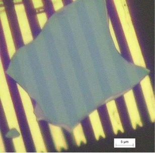
Figure 1. Temperature T dependence of the sheet resistance Rs
measured at 0 T for the ultrathin 2H–NbSe2 sample. The black and
blue arrows represent the superconducting (T c ) and CDW transition
temperature (TCDW ), respectively. Top insert: the differentiate
resistance dRs /dT vs T. The dRs /dT shows a dip at TCDW . Bottom
insert: optical image of the ultrathin 2H–NbSe2 sample. The scale
bar is 5 µm. The Rs is measured through electrodes numbered 1, 2, 3
and 4, and the two-point measurements through electrodes
numbered 2 and 3.
material [17] to an anisotropic single-gap in thin-film [16]. In
addition, monolayer NbSe2 exhibits a dramatic in-plane upper
||ab
critical field (Hc2 ) more than six times the Pauli paramag-
netic limit, which is related to competition between the large
intrinsic spin–orbit interactions (SOI) in monolayer NbSe2
and the Zeeman effect [18]. On the other hand, the TCDW Figure 2. (a) The superconducting transition at magnetic field H
increases significantly from 33 K in the bulk to 145 K in a ranging from 0 T to 2 T (the step is 0.1 T between 0 and 1.6 T).
single layer [1] and a CDW gap of ∆ = 4 meV at the Fermi The T c is defined as the temperature at which the resistance arrives
energy [2]. at 95% of the normal state resistance as shown by the dashed line.
(b) Left axis: the H–T phase diagram of the ultrathin 2H–NbSe2
In this paper, by using the mechanically exfoliation method
sample. The red symbols are the T c and the black symbols are the
and our electrode transfer technique, we fabricate the ultrathin T c0 . Right axis: the difference between T c and T c0 .
2H–NbSe2 samples and carry out detailed transport measure-
ments. The sample shows T c = 4.3 K and TCDW = 70 K. We
found its superconducting gap is ∆ = 1.1 meV at 0 K and the (I–V) measurements of the 2H–NbSe2 device are performed
gap features persist in the normal state, suggesting that a pos- by using Quantum Design Electrical Transport Option (ETO).
sible precursor superconductivity arises in ultrathin monolayer
2H–NbSe2 .
3. Discussion
2. Experiment Figure 1 shows the temperature T dependence of sheet
resistance (Rs ) of the ultrathin 2H–NbSe2 at zero applied field.
The 2H–NbSe2 device is fabricated based on the mechanical The optical image of the ultrathin 2H–NbSe2 device is exhib-
exfoliation method [19] and the developed electrode transfer ited in the bottom inset of figure 1. The Rs is measured through
technique [20]. The fabrication process is performed in a glove the electrodes numbered 1, 2, 3 and 4, and two-point measure-
bag filled with argon gas. First, the bulk single-crystal 2H– ments through the electrodes numbered 2 and 3, which show
NbSe2 (commercial crystals, Prmat (Shanghai)) is cleaved into a similar oscillation and superconducting gap value as the pair
layers with scotch tape, and pressed against a Si/SiO2 sub- of electrodes numbered 3 and 4 (data are not shown here). On
strate. Then, the thin 2H–NbSe2 flakes are distinguished under cooling down, the Rs decreases with the T, showing a convex
an optical microscope by the color. After that, the Au elec- at TCDW and jumping abruptly to zero at T c = 4.3 K. The con-
trodes prefabricated on the polyvinyl alcohol (PVA) film are vex of Rs at TCDW can be clarified in the top inset of figure 1,
accurately transferred onto the top of the selected flake of 2H– where dRs /dT vs T exhibits a dip at TCDW = 70 K. Such a dip
NbSe2 by using a sample transfer stage under the microscope. in dRs /dT was attributed to the CDW transition [1]. It is worth
Alternating current (AC) resistance and current versus voltage noting that the TCDW = 70 K observed here is much higher
2Supercond. Sci. Technol. 34 (2021) 025019 L B Lei et al
Figure 3. (a) The voltage—current (V–I) cures measured at T = 2 K, H = 0 (black curve) and 5 T (orange curve). (b) The differentiate
conductance dI/dV vs V for H = 0 and 5 T. (c) The dI/dV measured at the applied field H ranging from 0 to 3 T. The dI/dV vs V under 0 T
and below T c (d) and above T c (e). The curves are vertically shifted for clarity. (f) The T dependence of zero bias conductance peak (ZBCP)
normalized by the normal state conductance at 4.5 K (left axis) and the voltage (Vdip ) at the conductance dip (right axis).
than 35 K for bulk 2H–NbSe2 , consistent with the previous For the sake of investigating the superconducting gap,
reports that the reduced dimension in 2H–NbSe2 enhances the two-point measurements are performed on the sample and the
TCDW . [1] Since the reduced thickness induces the opposite results are displayed in figure 3. Figure 3(a) shows the current–
tendency of TCDW and T c , it thus suggests that the CDW order voltage (V–I) curve measured at temperature T = 2 K with
most likely competes with the superconducting order. applied field H = 0 and 5 T. It is found that the V shows a non-
Figure 2(a) shows the Rs (T) around the superconducting linear behavior with I at zero field, and a linear behavior at
transition regime under various magnetic fields H from 0 to 5 T. The non-linear V–I can be understood in terms of Andreev
2 T. The magnetic field H is applied in the c direction of reflection [21] from the proximity effect of the superconduct-
crystalline. The T c (red arrow in figure 2(a)) is defined as or/Au electrode junction. The linear V–I reflects the ohmic
the temperature where the resistance arrives at the value of behavior of the normal state. To clarify , one can differentiate
95% normal state resistance as shown by the dashed line. the V–I curve to obtain differentiated conductance dI/dV as
The T c0 is the zero resistance transition temperature as indic- plotted in figure 3(b). The dI/dV at 0 T shows the peak around
ated by the black arrow. The left axis of figure 2(b) is the the zero bias voltage and several dips at the higher voltage.
H dependence of T c and T c0 obtained from figure 2(a). The Actually, a maximum in dI/dV close to zero bias was previ-
difference between T c and T c0 is shown in the right axis of ously observed in point-contact measurements with a metal-
2(b), which increases with the applied field, suggesting that lic/superconducting point contact [23]. Such a behavior can
the superconducting transition is broadened by the applied be understood as a consequence of Andreev reflection (AR).
field. AR occurs at the interface between the normal metal and the
3Supercond. Sci. Technol. 34 (2021) 025019 L B Lei et al
likely results from non-ballistic limit contact of electrodes
with a superconductor. On the other hand, the dI/dV at 5 T
remains unchanged with the increasing V suggesting a good
ohmic contact between Au electrodes and 2H–NbSe2 .
Figure 3(c) shows the dI/dV vs V behavior in the various
magnetic fields. At 0 T, the dI/dV shows a peak around the zero
bias voltage and several dips at large V. It decreases with the
increase of H and finally becomes unresolvable above 2.4 T.
The large dI/dV peak below T c is attributed to Andreev reflec-
tion with a high transparency of interfaces [21], which will
be shown in figure 4. In order to get more accurate data of
dI/dV, we apply a direct current (DC) and alternating current
(AC) 0.01 mA on the samples. The obtained differential res-
istances dI/dV under different DC voltage bias are shown in
figure 3(d). It is found that both the conductance peak and
dip are suppressed as the temperature increases, while the
feature of the gap (marked by the arrows at Vdip in the con-
ductance dip) persists in the normal state up to 7 K as shown
in figure 3(e). The gap behavior was also found above T c
in other two-dimensional (2D) superconductors, like the thin
film of NbN [24] and LaAlO3 –SrTiO3 interface, [25] owing to
Cooper-pair localization driven by the disorder. [26] In con-
trast to the low-disorder NbSe2 van der Waals heterostructure
where there are no signs of persistence of gap-like features
above T c , [16, 22] our sample taking the polymers as protect-
ive encapsulating layers can induce substitutional defects and
impurities [27], which may lead to a strong disorder and local-
ized Cooper-pairs above T c . Thus the gap-like feature above T c
in figure 3(e) reflects the possible precursor superconductivity
in the normal state. In addition, the possible precursor super-
conductivity might not be related to the CDW order, since we
do not find the gap-like feature present above T c = 7 K at the
Figure 4. (a) The differential conductances (hollow symbols) at
T = 2–3.5 K and the fitting curves (solid lines) by BTK formula. bulk NbSe2 (data are not shown here), where the CDW order
(b) T dependence of superconducting gap ∆. (c) The temperature still survives. The zero biased conductance peaks are sum-
dependence of fitting parameter Γ (left axis) and Z (right axis). marized in figure 3(f). The left axis of figure 3(f) shows the
Error bars are given by the uncertainty of fitting. zero bias conductance peak (ZBCP) which is normalized at the
value at 4.5 K. It is found that the ZBCP decreases abruptly at
around T c = 4.3 K from 1.6 to around 1, suggesting the dis-
superconductor, where an incident electron with energy less appearance of Andreev reflection. On the other hand, the gap-
than the superconducting energy gap (∆) can be reflected back like feature characterized by the Vdip still survives above T c as
as a hole along a path of the incident electron (retro-reflection). shown in the right axis of figure 3(f).
Thus, AR enhances subgap conductance and leads to the max- Figure 4(a) shows the normalized differential conduct-
imum or peak in dI/dV. On the other hand, AR is absent in the ances (hollow symbols) (dI/dV)SC /(dI/dV)N versus V/2 for
insulator/superconductor interface, e.g. h-BN/NbSe2 structure ultrathin 2H–NbSe2 at 0 T and the T = 2 − 3.5 K, where
[16], which results in a dip in dI/dV at zero bias. Interestingly, (dI/dV)N is the differential conductance at 4.5 K. It is worth
in a graphene/superconductor structure, like graphene/NbSe2 , noting that the voltage on the junction of Au electrodes
the retro and specular AR are expected to occur at Fermi and 2H–NbSe2 is roughly one half of the applied voltage
energy (EF ) ≫ ∆ and EF ≪ ∆, respectively [22]. By tuning V between two Au electrodes. Thus, we fit the data using
EF of graphene through applying a gate voltage, the dI/dV at the BTK model in one anisotropic gap [28], which relates
zero bias is found to vary from the dip to the peak, which the normalized differential conductances to superconducting
corresponds to a change from specular and retro AR [22]. In gap values ∆, broadening parameter Γ and barrier paramet-
addition, a possible explanation for these conductance dips at ers Z, and display the fitting curves as the solid lines shown in
higher voltage is that the contact is not in the ballistic limit figure 4(a). Almost constant Z = 0.24 is used for fitting con-
at which the Vdip should decrease with the increase of tem- ductance curves. Note that Z describes the transparency of the
perature and magnetic field [23]. In our sample, the contact interface and a value of Z much less than 1 suggests a high
area between gold and NbSe2 is on a micrometer scale, where transparency barrier. The temperature dependence of broad-
both ballistic and non-ballistic limit contacts are expected to ening parameter Γ and gap ∆ are also shown in figure 4(b)
contribute to the conductance in parallel. Thus, the Vdip most and the left axis of figure 4(c). The gap ∆ exhibits BCS-like
4Supercond. Sci. Technol. 34 (2021) 025019 L B Lei et al
behavior with ∆(T = 0 K) = 1.1 meV. Here, the error bars References
are defined as the uncertainty due to the fit. We compare
the data fitted with anisotropic and isotropic gap formula, [1] Xi X, Zhao L, Wang Z, Berger H, Forró L, Shan J
and Mak K F 2015 Nat. Nanotechnol. 10 765–9
and find there are no differences between them. The value
[2] Ugeda M M et al 2016 Nat. Phys. 12 92–7
of 1.1 meV obtained here is consistent with the literature [3] Wang H et al 2017 Nat. Commun. 8 1–8
report where ∆(T = 0 K) = 1.3 meV for bulk 2H–NbSe2 is [4] Xing Y et al 2017 Nano Lett. 17 6802–7
reduced to 0.96 meV for three-layer 2H–NbSe2 . [16] Note that [5] Grüner G 1988 Rev. Mod. Phys. 60 1129
the ∆(T = 0 K) = 1.1 meV and T CDW = 70 K in our ultrathin [6] Chang J et al 2012 Nat. Phys. 8 871–6
[7] Achkar A et al 2012 Phys. Rev. Lett. 109 167001
2H–NbSe2 suggest the number of NbSe2 layers is around five,
[8] Comin R et al 2014 Science 343 390–2
while the T c = 4.3 K would correspond to one or two layers. [9] da Silva Neto E H et al 2014 Science 343 393–6
These discrepancies are most likely due to the sample quality [10] Wilson J A, Di Salvo F and Mahajan S 1975 Adv. Phys.
of our ultrathin 2H–NbSe2 being not so good owing to the use 24 117–201
of polymers as protective encapsulating layers in this work, [11] Moncton D, Axe J and DiSalvo F 1975 Phys. Rev. Lett.
34 734
which can lead to doping and damaging at the interface [27]
[12] Berthier C, Molinié P and Jérome D 1976 Solid State
and suppress the T c . Commun. 18 1393–5
[13] Cho K et al 2018 Nat. Commun. 9 1–9
[14] Staley N E, Wu J, Eklund P, Liu Y, Li L and Xu Z 2009 Phys.
4. Conclusion Rev. B 80 184505
[15] Cao Y et al 2015 Nano Lett. 15 4914–21
In summary, detailed electrical transport measurements are [16] Khestanova E et al 2018 Nano Lett. 18 2623–9
carried out on the ultrathin 2H–NbSe2 single crystal. The [17] Noat Y et al 2015 Phys. Rev. B 92 134510
T c = 4.3 K and TCDW = 70 K in the ultrathin sample. A [18] Xi X, Wang Z, Zhao W, Park J H, Law K T, Berger H,
Forró L, Shan J and Mak K F 2016 Nat. Phys.
good contact interface is found between Au electrodes and 12 139–43
ultrathin 2H–NbSe2 . A BCS-like gap with ∆ = 1.1 meV at [19] Geim A K and Novoselov K S 2010 The rise of graphene
0 K is revealed in this sample. The gap-like feature is found Nanoscience and Technology: A Collection of Reviews
to persist in the normal state up to 7 K. Our results suggest From Nature Journals (Singapore: World Scientific)
that possible precursor superconductivity arises in ultrathin pp 11–19
[20] Zhang C, Hu T, Wang T, Wu Y, Yu A, Chu J, Zhang H, Xiao
2H–NbSe2 . H, Peng W, Di Z et al 2020 (arXiv: 2006.03338
[cond-mat.supr-con])
[21] Andreev A 1964 Sov. Phys. JETP 19 1228
Acknowledgments [22] Efetov D K et al 2016 Nat. Phys. 12 328–32
[23] Sheet G, Mukhopadhyay S and Raychaudhuri P 2004 Phys.
The authors acknowledge the support of NSCF Grant No. Rev. B 69 134507
11574338, NSAF Grant No. U1530402 and CAS State Key [24] Sacepe B, Chapelier C, Baturina T I, Vinokur V M,
Baklanov M R and Sanquer M 2010 Nat. Commun.
Laboratory of Functional Materials for Informatics.
1 1–6
[25] Richter C et al 2013 Nature 502 528–31
ORCID iDs [26] Sacépé B, Dubouchet T, Chapelier C, Sanquer M, Ovadia M,
Shahar D, Feigel’Man M and Ioffe L 2011 Nat. Phys.
7 239–44
W Peng https://orcid.org/0000-0002-9888-1891 [27] Jung Y et al 2019 Nat. Electron. 2 187–94
H Xiao https://orcid.org/0000-0001-8859-9967 [28] Hayashi N, Ichioka M and Machida K 1996 Phys. Rev. Lett.
T Hu https://orcid.org/0000-0003-0338-9632 77 4074
5You can also read