THz Mixing with High-TC Hot Electron Bolometers: a Performance Modeling Assessment for Y-Ba-Cu-O Devices - MDPI
←
→
Page content transcription
If your browser does not render page correctly, please read the page content below
Article
THz Mixing with High-TC Hot Electron Bolometers: a
Performance Modeling Assessment for Y-Ba-Cu-O
Devices
Romain Ladret 1, Annick Dégardin 1, Vishal Jagtap 1,2 and Alain Kreisler 1,*
1 CentraleSupélec, CNRS, Univ. Paris-Sud, Université Paris-Saclay, Sorbonne Université, Group of Electrical
Engineering, GeePs, 91190 Gif sur Yvette, France; romain.ladret@gmail.com (R.L.);
annick.degardin@centralesupelec.fr (A.D.); vishal.jagtap@centralesupelec.fr (V.J.)
2 Institute for High Frequency and Communication Technology, University of Wuppertal, Wuppertal
D-42119, Germany; jagtap@uni-wuppertal.de
* Correspondence: alain.kreisler@centralesupelec.fr; Tel.: +33-1-6985-1651
Received: 15 December 2018; Accepted: 24 January 2019; Published: 25 January 2019
Abstract: Hot electron bolometers (HEB) made from high-TC superconducting YBa2Cu3O7–x (YBCO)
oxide nano-constrictions are promising THz mixers, due to their expected wide bandwidth, large
mixing gain, and low intrinsic noise. The challenge for YBCO resides, however, in the chemical
reactivity of the material and the related aging effects. In this paper, we model and simulate the
frequency dependent performance of YBCO HEBs operating as THz mixers. We recall first the
main hypotheses of our hot spot model taking into account both the RF frequency effects in the
YBCO superconducting transition and the nano-constriction impedance at THz frequencies. The
predicted performance up to 4 THz is given in terms of double sideband noise temperature TDSB
and conversion gain G. At 2.5 THz for instance, TDSB 1000 K and G 6 dB could be achieved at
12.5 W local oscillator power. We then consider a standoff target detection scheme and examine
the feasibility with YBCO devices. For instance, detection at 3 m through cotton cloth in passive
imaging mode could be readily achieved in moderate humidity conditions with 10 K resolution.
Keywords: THz heterodyne mixer; hot electron bolometer; Y-Ba-Cu-O high-TC superconductor; hot
spot model; RF local power distribution; THz impedance; noise temperature; conversion loss;
standoff detection prediction; passive imaging
1. Introduction
First considered by Gershenzon et al. [1], the superconducting hot electron bolometer (HEB)
principle was applied by these authors to low-TC (TC is the superconducting critical temperature)
and high-TC HEBs, Nb and YBa2Cu3O7–x (with x lower than 0.2, and called YBCO hereafter),
respectively. The concept then fruitfully evolved [2], rather in favor of low TC devices to start with,
mainly Nb and NbN, exhibiting the diffusion cooled and phonon cooled processes, respectively [3].
In fact, the research on HEBs was mainly driven by immediate applications to THz radio astronomy
as mixers for heterodyne reception [4,5]. Besides, YBCO was attractive in several respects, e.g.,
operating temperature with light cryogenics, or fast response, due to its very short electron-phonon
relaxation time ep, in the ps range [6–8]. Early YBCO HEB mixers were demonstrated at mm-wave
[9–12] or THz [9,10,13–15] frequencies. Difficulties were encountered, however, which mainly arose
from YBCO chemical reactivity to atmospheric water and carbon dioxide and to the fabrication
process as well, which compromised the durability of good performances for frequency mixing
operation [16]. They also arose from the superconducting film to substrate phonon escape time esc,
Photonics 2019, 6, 7; doi:10.3390/photonics6010007 www.mdpi.com/journal/photonics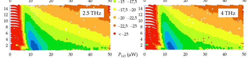
Photonics 2019, 6, 7 2 of 26
much longer for YBCO [17] than for Nb, for instance [18], with a detrimental effect on the
instantaneous bandwidth [11–13,19]. More recently, MgB2 has met a sustained interest as a
compromise between NbN and YBCO, in terms of operating temperature, but also in terms of
instantaneous bandwidth [20,21].
The just mentioned experimental work was permanently sustained by modeling and simulation
efforts to predict and interpret HEB performance. We now introduce those performance simulation
aspects, because they indeed are our main concern in the present article.
Several steps in the HEB modeling approach have to be considered. In the "0D" or point
bolometer model, only energy transfer between thermal reservoirs is evaluated. In the
superconducting material (Figure 1a), the electron reservoir at temperature Te interacts with the
phonon reservoir at temperature Tp; this interaction is governed by the above-mentioned
electron-phonon relaxation time ep. The phonons release their energy to the device substrate with
the above-mentioned escape time esc [22]. If the electron-electron interaction time ee is much shorter
than ep, (which is the case for Nb, NbN or YBCO), hot electron bolometric action occurs, such that Te
> Tp, provided that esc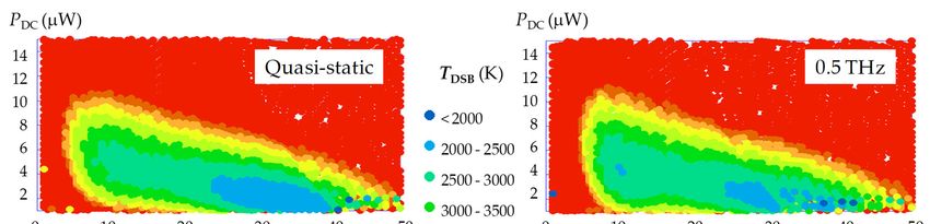
Photonics 2019, 6, 7 3 of 26
YBCO HEB constriction (of length L, width w, and thickness ) connected to the arms of a THz planar
antenna.
2. Models and Methods
2.1. Describing the Superconducting Transition at THz Frequencies
To have access to the resistance (and, more generally, the impedance) vs. electron temperature
Te of the YBCO constriction at angular frequency = 2f, we describe the superconductor by a
two-fluid (2F) model. The concentrations of the superconducting and normal charge carriers are nS
and nN, respectively, with nS + nN = n, the total free electron concentration [28]. Defining the two-fluid
critical temperature TC2F, the dependence of nN/n = fN(tr) as a function of reduced temperature tr =
Te/TC2F was chosen as fN(tr) = tr4. This choice minimizes the electron system free energy, according to
the Gorter-Casimir 2F model [28]. Hence the real and imaginary parts of the complex conductivity
= 1 j2, assuming Ohm's law is still valid in an impurity scattering description [29]:
2 1 r2
tr 1 : 1 Ntr4
r
, 2
0 02 1 r 2
1 t ,
4
r (1a)
tr 1 : 1 N , 2 0, (1b)
where N is the normal state conductivity, r = S is the impurity scattering parameter (for scattering
time S), 0 is the permeability of a vacuum and 0 is the London's penetration depth at tr = 0.
As the two-fluid model depicts a homogeneous superconducting material, we have to describe
the experimentally observed broadening of the superconducting transition; such a broadening is
related to the film microstructure (e.g., grain boundary weak links). This is performed by
introducing a Gaussian distribution of critical temperature values, centered at the mid-transition
critical temperature TC0, as discussed in Reference [27], with
T T 2
1 e C0
g exp , (2)
GN 2 T 2
G
where GN is a normalization coefficient and TG is the critical temperature standard deviation, to be
adjusted to fit the experimental transition.
After having expressed the two-fluid resistivity 2F ( ) 12F ( ) j 22F ( ) 1 , we then fit the
experimental DC resistivity transition [30] as a convolution product between 12F ( 0) and the
Gaussian function, so that
1exp Te , TC0 , ΔTG 12F 0 g Te , TC0 , ΔTG . (3)
The so-obtained transition is then approximated by a Fermi-Dirac type function, as more
appropriate to further numerical treatments (see below Section 2.2, hypothesis 8).
To obtain the THz dependence, we introduce 2F() in the so-obtained DC transition, and then
fit a new Fermi-Dirac-like transition with frequency dependent parameters (mid-transition
temperature, transition width and minimum resistivity, as detailed in Section 3.1) [27].
2.2. HEB Master Equations
For an HEB constriction of volume VC = L w (Figure 1b), the thermal power balance is
governed by the heat diffusion equations for the electron and phonon baths, represented by
Equation (4a,b), respectively, as follows: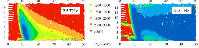
Photonics 2019, 6, 7 4 of 26
V
Te
V C
n
Te VC Ce Te Tp
n
L
PJ-tot, (4a)
x C e
x C e
t n 1 x
n epTec
V
Tp
VC C p
Tp VC C p Tpm T0m VC Ce Ten Tpn
,
(4b)
x C p x t m 1
m escTpc n epTenc1
where indices e and p pertain to the electrons and phonons of the superconducting film, respectively
(Figure 1a). e and p are the corresponding thermal conductivities, Ce and Cp the unit volume
specific heats (evaluated at temperatures Tec and Tpc, respectively). Integers n and m characterize the
thermal exchanges between electrons and phonons and phonons and substrate (at reference
temperature T0), respectively. The source term in Equation (4a) represents the Joule power locally
injected in a constriction slice of width x. This power results from both DC and THz currents
flowing along the constriction of cross-sectional area SC = w . More specifically, after having
dropped the higher order terms:
(0, Te ( x)) (LO , Te ( x)) 1
I 02 x LO I S cos (LO S )t x.
PJ-tot 2 I
I LO (5)
SC SC 2
In this equation, I0 is the DC bias current, ILO (local oscillator) and IS (signal) are the THz current
amplitudes at angular frequencies LO and S, respectively. The resistivity functions are deduced as
discussed in Section 2.1. It therefore appears that (i) the current components are constant over SC (see
below, hypothesis 2) and (ii) the knowledge of Te(x) is required; this implies an iterative resolution
procedure for the coupled Equation (4a,b).
The hypotheses governing the resolution of Equation (4a,b) are given in the following list.
1. These equations obviously describe a phonon cooling mechanism for the electrons in YBCO, as
opposed to Nb HEBs, where cooling by electron diffusion to the metal contacts is the dominant
process [3,31]. In fact, using YBCO data (cf. Section 3.2, Table 1), we evaluate the electron
diffusion length le (epe/Ce)1/2 25 nm, a significantly smaller value than the constriction
length (100 to 400 nm) considered here, so that phonon cooling will prevail [22].
2. It also appears from Equation (5) that the DC and THz current densities are assumed to be
constant across the area SC, a point discussed at length in Reference [32]. Due to the resistivity
vs. Te(x) dependence, DC and THz powers are non-uniformly absorbed along the constriction,
as noticed in Reference [33].
3. The constriction ends (at coordinates x = 0 and x = L) are at reference temperature T0, which is
the cryostat / cryogenerator cold finger temperature (gold antenna contacts). So that: Te(0) =
Tp(0) = Te(L) = Tp(L) = T0.
4. The solutions Te(x) and Tp(x) follow the geometrical symmetry of the constriction with respect
to its center: Te(x) = Te(L x) and Tp(x) = Tp(L x). Consequently, the equation solving will be
performed in a half-constriction, e.g., x [L/2, L].
5. The dissipated power in the constriction tends to raise Te(x) and Tp(x), which will reach their
maximum values at the constriction center, so that: Temax = Te(L/2), and Tpmax = Tp(L/2), with
dTe(L/2)/dx = dTp(L/2)/dx = 0.
6. The energy exchange exponent n = 3 was taken for YBCO, as extracted from electron-phonon
interaction time measurements (see, e.g., Reference [1]). The YBCO to substrate phonon
mismatch index m = 3 resulted from the number of available phonon modes, proportional to T3
(Debye's model).
7. The YBCO to MgO substrate phonon escape time was deduced as esc (ps) = 75 (nm) [17]. In
the case of PBCO/YBCO/PBCO trilayer constriction [30], where PBCO lies for PrBa2Cu3O7–y, a
correction should be applied to , as considered in Reference [13].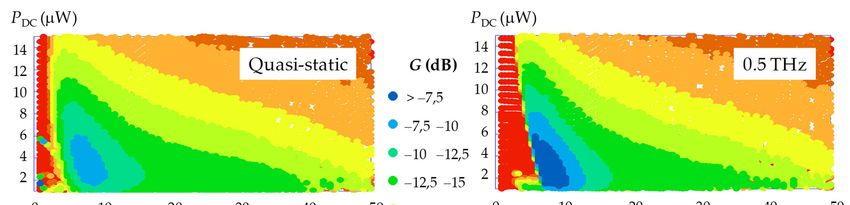
Photonics 2019, 6, 7 5 of 26
8. For numerical computation convenience, the resistive superconductive transition has been
approximated by a Fermi-Dirac function of the form = 0 [1 + exp((TC − Te) / T)]−1, to fit the
variation given by Equation (3).
9. Due to thermal effects, TC is sensitive to the constriction DC bias current IDC; this effect has been
taken into account by writing TC(IDC) = TC(0)[1 − (IDC/(JrefSC))2/3], where Jref is a reference current
density. This point is mentioned in Reference [25] and discussed in Reference [34], in the context
of YBCO thin film electrical transport vs. microstructure relationship.
10. Because we can have access to the constriction RF impedance, it was possible to handle the
effective power dissipated in the constriction as α PLO, with α = αimp α', where αimp is the
impedance matching factor between the constriction and the antenna, and α' represents all the
losses from other origins (focusing optics, diplexer, etc.).
2.3. Solving HEB Master Equations
In the two aforementioned Equation (4a,b), we set certain parameter values to limit to two the
number of variables to find by the iterative solving method. The known parameters are VC, e, Ce, n,
ep, α', SC, p, Cp, m, esc. Formally, the fixed (input) variables are PLO, I0 and T0, because in a
measurement procedure, these are the parameters controlled by the operator. The resolution of the
equations should therefore be performed on the (output) variables Te(x) and Tp(x), and their second
derivatives d2Te/dx2 and d2Tp/dx2 as well.
All the above considerations give enough information that the second derivatives can be
deduced at each point by our program when x varies from L/2 to L. Similarly, Te(x) and Tp(x) are
deduced at each point provided that we define Temax and Tpmax, where the relation Temax ≥ Tpmax will
help us to converge. The basic resolution approach is therefore to test (Temax, Tpmax) pairs until the
value found at the extremity of the constriction is: Te(L) = Tp(L) = T0, which represents our criterion of
success for the calculation.
Furthermore, we have made a significant improvement of this basic resolution process, by
exchanging the roles of Temax and I0, such that Temax is now a fixed parameter and I0 a computational
variable. This "trick" facilitates the calculations, because, on the one hand, the Tpmax solution search is
carried out with a fixed upper bound (Temax is known). On the other hand, difficult cases where
different constriction resistance (R) values can be associated with the same I0 value (because I0 is
surjective towards R), can be simplified: In fact, Temax is strongly correlated with the resistance
(because Temax is bijective with R in all our calculations).
Unlike the formal procedure just described, Equation (5) indicates that ILO (and not PLO) is the
THz input, PLO being deduced at the end of the calculation. Therefore, it is not possible to perform a
calculation that will accurately give a result ascribed to a given PLO value. What we obtained by our
method was a "cloud of points" where each of these points is a configuration of the HEB operating at
a certain power PLO, at a certain bias current I0 and having a certain resistance R (as well as all the
other characteristics that we wish to deduce).
The goal of our approach is to obtain a "cloud of points" as homogeneous as possible, in order to
extrapolate the operating configurations we are interested in. Typically, we recreated, by
interpolation, a series of points that are the I-V responses to the different PLO values we wished to
investigate (e.g., PLO [0, 50 μW]). With these new series of points, we were able to reuse the
processing tools for the calculation of the conversion gain and the noise temperature, as further
commented in Section 2.4.
The global solving loop process is summarized as follows. Starting with Equation (5), the local
heat power dissipation leads to the global heterodyne power mixing expression:
PJ-tot PDC αPLO 2α PLO PS cos LO S t ,
(6)
Photonics 2019, 6, 7 6 of 26
where appears the intermediate frequency (IF) IF = | LO − S |. As ILO is homogeneous along the
constriction, the RF heat dissipation PLO is then deduced from the ZRF = RRF + jXRF THz impedance.
The result is then fed back into Equation (5), according to:
2 PLO
ILO , (7)
RRF
the constriction resistance/reactance contributions being
L (0, Te ( x)) L 1 (LO , Te ( x)) L 2 (LO , Te ( x))
RDC dx , RRF dx , and XRF dx. (8)
0 SC 0 SC 0 SC
It should be noticed that in Equation (7), α = αimp α' (hypothesis 10 above) is a function of ZRF,
through the impedance matching coefficient
2 Re( Z )
ZRF Za*
imp 1 RF
, (9)
ZRF Za ZRF
where Za is the antenna impedance. The left hand term is the regular impedance matching
expression, whereas the right hand term is a correction ratio between the RF power dissipated in the
constriction and the total input power.
For a self-complementary antenna, Za = Ra + jXa is purely real, with
60
Za Ra , (10)
1 r 2
where r is the substrate material dielectric constant [35,36].
2.4. HEB Mixer Performance
2.4.1. General Considerations and Conversion Gain
For the calculation of the mixer conversion gain and noise temperature, it is necessary to
discriminate between: (i) The contribution originating from the DC bias power PDC, and (ii) the
contribution originating from the RF power (PLO and PS). To do this, we first define two parameters
KDC and KRF as:
R
KDC ( PLO 0), (11a)
PDC
R
KRF ( PDC 0), (11b)
PLO
where R is the constriction resistance (evaluated according to the adopted model), and assuming PS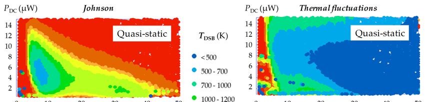
Photonics 2019, 6, 7 7 of 26
RL I 2 / 2 2 I 02 RL KRF
2 P
LO
G 2
PS K DC I 02 RL R0 (13)
2
R0 RL 1
RL R0
where R0 = R R and I0 is the constriction current when PS = 0.
It is to be noticed that the gain is also involved in the noise expression. Let us consider the noise
measured at the mixer input (index "in") and the noise measured at the mixer output (index "out");
the corresponding relationship for the noise temperatures is Tin = Tout/G.
2.4.2. Noise Temperature Contributions
The two main noise contributions of internal origin in a superconducting HEB are the Johnson
(Jn) noise and the thermal fluctuation (TF) noise [3,37].
Johnson noise is considered as an additional voltage source vJn in series with the bolometer,
such that 2 4k T R f , where f is the output signal bandwidth. In this context, v introduces
vJn B 0 0 Jn
variations RJn and Jn , hence the noise power PJnout k BTJnout f dissipated in the mixer load
resistance RL. Using the conversion gain expression (Equation (13)), one readily obtains the dual
sideband (DSB) expression of the mixer input Johnson noise:
in
R0T0
TJn,DSB 2
. (14)
I 0 KRF PLO
The noise spectral density originating from thermal fluctuations of the electrons involves the
electron-electron interaction time τee and is expressed as follows [24]:
4k BTe2 ee
Te . (15)
Ce VC
A current out k T out f dissipated in
results from these fluctuations hence the noise power PTF
TF B TF
the load resistance RL. In the same manner as previously, one obtains the DSB expression of the
mixer input thermal fluctuation noise:
2
in 1 dR Te2
TTF,DSB 2 ee . (16)
KRF PLO dTe Ce VC
The global expression of the mixer noise temperature is therefore
in in in
TIF
TN,DSB TJn,DSB TTF,DSB , (17)
2G
where we have introduced the IF amplifier output noise temperature TIF, hence the approximate
expression TIF/2G for the DSB input noise temperature. Besides, we have considered here TIF as
independent of the working frequency and equal to the cooling temperature T0 of the HEB [38].
In practice, the mixer performance can be accessed by widespread techniques, such as the
Y-factor method [39], which consists in using a blackbody (BB) source alternately adjusted at
temperatures TBB = Thot or Tcold, and placed at the mixer input. Defining Y = (Phot/Pcold)out as the ratio
between the associated mixer output powers (in the mixer bandwidth f), one obtains for the mixer
input noise TNin = (Thot YTcold)/(Y 1) in the Rayleigh-Jeans limit [39]. Moreover, the mixer gain is
equal to the slope of the Pout vs. kBTBBf straight line plot (kB is the Boltzmann constant).
2.5. Standoff Detection Implementation with an HEB Heterodyne Detector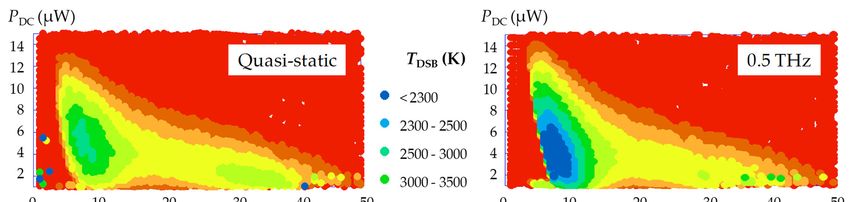
Photonics 2019, 6, 7 8 of 26
Passive imaging techniques rely both on collecting naturally emitting radiation from a scene
and detecting the contrast between warmer and colder targets. The human being exhibits an
emissivity of about 95% at frequencies above 600 GHz, which makes such a target appear warm
relatively to a metal object of low emissivity.
We have checked the feasibility of standoff target detection operating in the passive mode with
a YBCO HEB THz mixer. We have considered the simplified schematic in Figure 2, which illustrates
losses of various origins. The noise equivalent power (NEP) requirement for the detector was
deduced from the blackbody power PBB emitted by a target of area AT and collected by a detector of
area AD (the HEB focusing lens effective area). For a receiver of bandwidth 2 at center frequency 0
and for a temperature difference T to be resolved at Top, the power difference is
0 AD AT
PBB ( , T ) B (Top T ) B (Top ) d T , (18)
0 dT2
where B(T) is the blackbody spectral radiance (in W∙m ∙ sr ∙ Hz ), T the target emissivity, and
dT the target to detector distance (possibly corrected to include imaging system primary and
secondary mirrors).
Figure 2. Simplified schematic for HEB standoff THz detection arrangement. The target resolved
area is deduced from the Airy pattern at the HEB location (Equation (19)).
The NEP was then obtained by assuming the resolution to be diffraction limited for the detector
(i.e., at the focusing lens focal plane). Consequently, the resolved distance at the target can be related
to the Airy disk diameter at the detector focal plane by a factor dT/fL, approximately, where fL is the
focal length of the focusing lens. We finally work out at wavelength :
0
B (Top T ) B (Top ) d
0 1.22
2
(19)
NEP T topt tatm tobs ,
int 2
where int = 1/(2int), int being the (e.g., post-detection) integration time; topt, tatm, and tobs are the
transmission factors related to optics, atmosphere and obstacles, respectively (Figure 2). These
factors are considered in the following.
topt includes the HEB planar antenna main lobe efficiency, the focusing lens and the detector
cryostat window losses, and the LO injection losses (diplexer or beam splitter).
tatm was extracted from the atmospheric attenuation factor atm (in dB/m) in various conditions,
using the Atmospheric Effects Model (AEM) described in Reference [40]. Such extracted values
were also in line with values deduced from data in Reference [41].
tobs represents the transmission through some obstacle existing in front of the target (cloth,
cardboard, etc.).
The double sideband noise temperature required for the HEB was deduced from the NEP in the
Rayleigh-Jeans limit as [39]: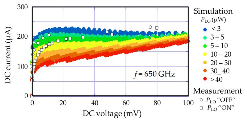
Photonics 2019, 6, 7 9 of 26
NEP
TDSB . (20)
2k B 2
3. Simulation Results
3.1. YBCO Superconducting Transition in the THz Range
As shown in Section 2.3, we have been able to link the experimental DC transition with a
two-fluid model representation of the resistive transition when 0. From this result, we perform
at terahertz frequencies a similar convolution as in Equation (3), which will therefore modify the
modeled resistive transition accordingly. We approach this modification as the combination of three
phenomena: The decrease of the average mid-transition critical temperature (TC), the widening of
the resistive transition (T) and the appearance of a minimum resistivity (min). To the first order, we
write:
TC(fTHz) = TC(0)(1 AT fTHz), (21a)
T(fTHz) = T(0)(1 + BT fTHz), (21b)
min(fTHz,tr = 0.8) 2min(fTHz,tr = 0) = CT fTHz. (21c)
In practice, the AT, BT and CT parameters are introduced in the expression of the resistivity
according to a Fermi-Dirac function (for convenience in our simulation). Their values are calculated
for a given material and approximated for the 0 to 5 THz frequency range. Thus, in a first step, it is
necessary to calculate CT from the expression of min deduced from 2F(,tr 0), as presented in
Equation (21c). The pair of parameters (AT, BT) is then calculated by determining the pair which
minimizes the difference function between the gaussian fit and the current resistivity function
|G(T, ) (T, )|, in both the 50 to 100 K and 0 to 5 THz ranges.
From an experimental point of view, our current technological process allows to achieve YBCO
constrictions of length and width L = w = 400 nm and thickness = 35 nm, with a mid-transition
critical temperature TC = 89 K [25,30], a transition width of 1.2 K and a conductivity N = 3.15 105
−1m−1. Such constrictions were made from YBCO films sputtered on MgO (001) single crystalline
substrates. X-ray diffraction confirmed the mainly c-axis orientation of the films, with rocking curves
exhibiting full width at half maximum values of ~ 0.18 degree for the (005) YBCO line. Weak
parasitic lines were observed however, which indexation could also confirm the presence of a-axis
growth [16]. The measured c-axis lattice parameter values ranged from 1.169 to 1.170 nm, which are
close to the value of fully oxygenated Y1Ba2Cu3O7 films [42]. Besides, in-plane twinning of the films
is expected [43]. The film surface morphology was uniform with a typical roughness of about 4.5 nm
rms independent of the YBCO thickness [44].
For a YBCO constriction exhibiting such dimensions, our simulation results lead to: AT = 0.011
THz−1, BT = 0.186 THz−1 and CT = 6.8210−8 ΩmTHz−1. Those results are illustrated in Figure 3.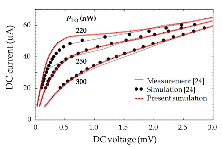
Photonics 2019, 6, 7 10 of 26
100 f (THz)
Dimensions 0 Gaussian
Constriction resistance ()
80 L = w = 400 nm 0.32 -
= 35 nm 0.64 -
1 -
60
2 -
4 -
40
0 Fermi-Dirac
0.32 -
20
0.64 -
T
C0 1 -
0 2 -
80 85 90 95
4 -
Electron temperature (K)
Figure 3. Frequency-dependent YBCO superconducting transition illustrated by the constriction
resistance vs. frequency. The DC plot (f = 0) is a fit from experiment [30]. The gaussian curves
describe the TC distribution as discussed in the text. Fermi-Dirac fits have been used for the device
performance simulation as more appropriate to the convergence of numerical solutions. Redrawn
after [27].
3.2. DC Characteristics
For our simulations, we have considered two HEB devices (data gathered in Table 1). The
constriction dimensions of device A are close to the limits achievable with e-beam lithography;
these dimensions are those considered in the "0D" HEB model [22]. The constriction dimensions of
device B are those achievable with our currently available technological process, combining optical
and e-beam lithography [25]. Device B is also the constriction example taken in Section 3.1.
3.2.1. Temperature Profiles
The temperature profiles (solutions of Equation (4a,b)), shown in Figure 4 for devices A and B
exhibit features, typically representing the HEB phenomena, namely: (i) The hot electron condition
Te(x) > Tp(x), and (ii) the hot spot (i.e., normal state) region xHS such that Te(x) > TC for x xHS. We
notice that Te(x) is closer to Tp(x) for device B; this is due to the stronger phonon film to substrate
escape efficiency, as testified by the 3.5 times longer esc value for device B (Table 1).
Table 1. For constrictions A and B, device characteristics and YBCO physical parameters used in the
simulations. Unless otherwise stated, the parameter values are those of [22].
L, w Ce Cp e p
Device
(nm) (nm) (Jm−3K−1) (Jm−3K−1) (Wm−1K−1) (Wm−1K−1)
A 100 10 2.5104 6.5105 1 10
B 400 35 2.5104 6.5105 1 10
ep esc N 1 JC 2 TC 3 T T0
Device
(ps) (ns) ( m )
–1 –1 (Acm–2) (K) (K) (K)
A 1.0 0.75 3.15105 2.2106 85 1.2 60
B 1.7 2.6 3.15105 2.2106 89 1.2 70
1 Normal state conductivity at 100 K. 2 Critical current density at 77 K. 3 Mid-transition critical temperature.Photonics 2019, 6, 7 11 of 26
90 90 90 90
T 188 A T
C 700 A
C
530 A
85 85
80 T 130 A T 80
e p
T (K)
T (K)
T (K)
T (K)
188 A 80 80
p
e
p
e
70 70
75 75
T T
e p
T
T 0
0
60 60 70 70
0 20 40 60 80 100 x (nm) 0 50 100 150 200 250 300 350 400 x (nm)
0 L/2 L
0 L/2 L
(a) (b)
Figure 4. For devices A and B, electron temperature Te(x) (solid curves) and phonon temperature
Tp(x) (dashed curves) profiles: (a) For device A (PLO = 5 W); (b) for device B (PLO = 35 W). T0 and TC
are the reference (cold finger) and mid-transition critical temperatures, respectively. Arrows on TC
lines delimit the hot spot regions xHS (see text). Curve labels indicate the DC bias current I0 values.
As a check of the validity of our simulation approach, we run our procedure with low-TC
material data for the NbN constriction considered in Reference [24]. We obtained Te(x) profiles very
close to each other (less than 5% difference). This was verified for various PLO values in the
quasi-static (QS) regime, i.e., at the low LO frequency limit of the constriction impedance (Equation
(8)).
3.2.2. Current-Voltage Plots
The Te(x) profile allows to have access to the resistivity profile along the constriction, hence to
the constriction resistance/impedance by integration (Equation (8)). As explained in Section 2.3, the
I-V plots can then be deduced in the form of "clouds of points". This representation illustrates, in
color/gray tone levels, the device DC response as a function of e.g., PLO, as shown in Figure 5 for
devices A and B.
With regard to device A, we notice that the I-V dependence can be hysteretic: For a given bias
current value, there are three distinct HEB voltage operating points. Indeed, in the 5 mV to 15 mV
range, the differential resistance is negative, this behavior being typical of HEBs operating at low T0
and exhibiting a short film to substrate escape time. Consequently, the largest voltage variations, as
PLO varies, where a larger part of the constriction is still superconducting, are situated below 30
mV. This effect is not observed for device B, due to the longer escape time in that latter case.
For further verification, we also compared, for an NbN device, our I-V results with those
reported in Reference [24]. As shown in Figure 6, the calculated values are close to the HEB
measurements at bias currents above 20 A. The result of our calculation for PLO = 220 nW is,
however, noticeably different from that reported in Reference [24]. This is seemingly due to the
difference in the computational method, but this difference does not affect the calculation of the
dynamic performances (conversion gain and noise temperature) of the HEB.Photonics 2019, 6, 7 12 of 26
(a) (b)
Figure 5. For devices A and B, DC current vs. DC voltage maps according to PLO values, at 400 GHz
LO frequency: (a) For device A (T0 = 60 ); (b) for device B (T0 = 70 ). Redrawn after [45].
Figure 6. For the NbN HEB reported in Reference [24], the comparison between I-V plots measured
on the fabricated device and simulation according to the model developed in Reference [24] and our
present model.
3.3. Mixer Performance
The noise temperature and the conversion gain were determined at given local oscillator power
PLO; they were deduced from the heat equations solving results and presented in the form of "clouds
of points" (see Section 2.3). To highlight the influence of PLO for a given DC bias power PDC, we have
illustrated those results as PDC vs. PLO maps. We have considered four operating frequencies: The
quasi-static (QS) regime, 500 GHz, 2.5 THz and 4 THz. The results are presented in the following.
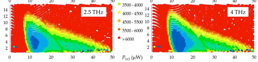
3.3.1. Noise Temperature
We observe in Figure 7 that the minimum noise PDC vs. PLO area evolves in level and that the
optimal PLO value also evolves (see Table 2 below). In particular, we notice that the secondary area of
low noise temperature, starting at PLO 35 μW in the QS mode, vanishes when the frequency
increases.
This consideration can be furthered by separating the sources of noise for the two cases of QS
regime and LO frequency at 2.5 THz (Figure 8). The contribution of each noise source informs us
about the evolution of the area where the noise is minimum. We notice that in the QS regime, the
fluctuation noise is minimal when PLO > 20 W, whereas at 2.5 THz the low noise area is distributed
differently, with improved noise level when 10 W < PLO < 15 W.Photonics 2019, 6, 7 13 of 26
Figure 7. For an HEB constriction of dimensions L = w = 400 nm and = 35 nm (Figure 1), maps
exhibiting double sideband noise temperature TDSB levels in DC bias power vs. LO power
coordinates. Impedance matching coefficient αimp with the antenna was included.
Figure 8. For an HEB constriction of dimensions L = w = 400 nm and = 35 nm (Figure 1), maps
exhibiting Johnson noise and thermal fluctuation noise contributions to TDSB levels in DC bias power
vs. LO power coordinates. Impedance matching coefficient αimp with the antenna was included.
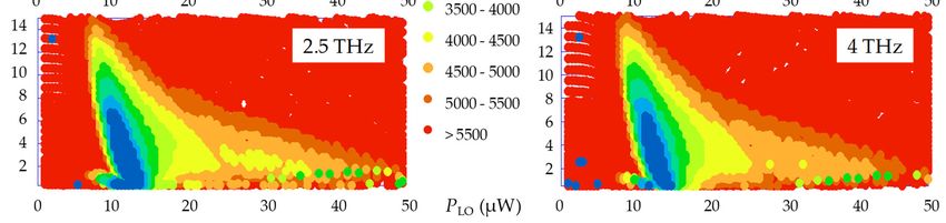
3.3.2. Conversion Gain and Summary of Mixer Results
We then resume the comparison for the conversion gain at the four working frequencies, as
shown below in Figure 9. The gain decreases as PDC increases, and is maximized at given PLO. Thus,
as the frequency of the local oscillator increases, the conversion gain appears to be maximum around
2.5 THz and requires a local oscillator power of 12.5 μW (see Table 2 below).
As compared to previous results [25], the present model highlights a sharp decrease in the local
oscillator power needed to operate the HEB at the optimum point. Intuitively, one might be inclined
to think that after taking into account αimp coupling losses, PLO should increase as 1/αimp. In fact, the
present model introduces two physical properties, namely the influence of the non-uniform
distribution of the dissipated LO power, and the impedance matching coefficient between the
antenna and the nano-constriction, which alter the response of the simulated HEB.Photonics 2019, 6, 7 14 of 26
Indeed, the dissipation of the radiofrequency current is concentrated in the resistive zone of the
nano-constriction, where dominates the dissipation by Joule effect (hot spot). Thus, if for example a
quarter of the nano-constriction is resistive, then the power will be mainly dissipated in this zone,
thus reducing a prerequisite of 35 μW (calculated in the model of the "regular" hot spot adapted to
YBCO [25]) down to 7.5 μW.
Figure 9. For an HEB constriction of dimensions L = w = 400 nm and = 35 nm (Figure 1), maps
exhibiting G levels in DC bias power vs. LO power coordinates. Impedance matching coefficient αimp
with the antenna was included.
Table 2. For an HEB of dimensions L = w = 400 nm and = 35 nm at different operating frequencies,
with matching coefficient αimp included, compared performances at an optimal operating point with
respect to the noise temperature.
Frequency IDC (A) R ()1 PDC (µW) PLO (W) G (dB) TDSB (K)
QS 454 21.3 4.4 7.5 −9.0 1781
500 GHz 464 21.4 4.6 7.5 −7.1 1208
2.5 THz 394 14.6 2.3 12.5 −6.1 1013
4 THz 379 13.0 1.9 13.5 −6.5 1093
1 RF resistance.
3.3.3. IF Bandwidth
Small signal analysis (as formulated in Reference [25]) was performed to determine the IF
response in terms of conversion gain as a function of the intermediate frequency fIF = (LO − S)/2, as
originating from the last term in Equation (5). This is illustrated in Figure 10 for devices A and B. The
main features are: (i) The low frequency regular bolometric response plateau, (ii) the regular
bolometric cutoff associated with the escape time esc, (iii) a second plateau characterizing the HEB
action, (iv) the HEB cutoff associated to the YBCO intrinsic relaxation time ep. Clearly, the
bandwidth is limited by the esc value (Table 1), which is in favor of ultrathin and small volume
constrictions [23,25]. It therefore appears that a bandwidth close to 1 GHz can be expected for device
A.Photonics 2019, 6, 7 15 of 26
0
Regular
-10
Conversion gain (dB)
bolometric
cut-off
-20
HEB plateau
-30
Device A
(P = 5 W)
-40 LO
Device B HEB cut-off
-50 (P = 12.5 W) ~1/2
LO ep
-60 6 7 8 9 10 11 12
10 10 10 10 10 10 10
Intermediate frequency (Hz)
Figure 10. For devices A and B, conversion gain vs. fIF, at PLO values minimizing TDSB. Data for device
A were available in the QS regime [25], whereas data at 2.5 THz were used for device B [45].
3.4. Standoff Detection Performances Requirements
We have run the simulation for the standoff system, as presented in Section 2.5 (Equations
(18)–(20)), with detector double sideband width 2 = 2 GHz and integration bandwidth int = 1 Hz.
Five frequencies centered in atmospheric transmission windows were considered: 670 GHz, 1.024
THz, 1.498 THz, 2.522 THz, and 3.436 THz. Besides, the detection scenario was chosen according to
the following parameters:
Target emissivity T = 1.
Optical losses were evaluated according to the antenna main lobe efficiency (−2 dB), the
focusing lens and the detector cryostat window losses (−1 dB), and the LO injection losses
(beam splitter: −3 dB), amounting to topt 24%.
tatm was determined for various relative humidity values (RH, in the 10% to 70% range) at
operating temperature Top = 295 K, at sea level and with clear atmospheric conditions (e.g., no
dust).
tobs was calculated for light cotton clothing from data in Reference [46] for frequencies below 1
THz, and in Reference [47] for frequencies above 1 THz. Values of tobs for the five selected
frequencies are collected in Table 3.
Various values of temperature resolution T were taken into account, from 0.5 K to 10 K, with
respect to the results obtained as a function of the pertinent parameters (frequency, target distance).
Figure 11a exhibits the required HEB mixer noise temperature for a passive mode detection
system as a function of frequency and atmospheric relative humidity level for a 10 m target distance
and a resolution T = 1 K. The influence of relative humidity strongly occurs at frequencies higher
than 2.5 THz (for instance, a low value of TDSB ≈ 85 K is required for a system operating at 2.5 THz at
RH level of 40 %). In order to reach a viable standoff passive detection operation with TDSB values
technologically reachable, it is therefore necessary to reduce either the target distance or the
temperature resolution.
Figure 11b exhibits the required noise temperature as a function of target distance and
resolution temperature at 2.5 THz and highly stringent RH level of 70%. Thus, for instance, at 5 m
target distance, the detection system would require TDSB ≈ 110 K for T = 1 K, a restrictive parameter
which could be relaxed to TDSB approaching 1100 K for T = 10 K.
Table 3. Transmission coefficient through an obstacle of light cotton cloth [46,47].
Frequency (THz) 0.67 1.02 1.49 2.52 3.44
tobs (%) 75 47 21 2 0.1Photonics 2019, 6, 7 16 of 26
5 4
10 10
10% Relative humidity
10%
4 70% 10% RH (10 % steps) 3
10 10 T = 1 K
(K)
(K)
70%
T = 5 K
70%
DSB
DSB
3 2 T = 10 K
10 10%
10
Required T
Required T
2 1
10 10 T = 295 K
T = 295 K 10% op
op
1 T = 1 K 0 0 = 2.5 THz
10 70% 10
d = 10 m RH = 70 %
T
0 70% -1
10 10
0.6 0.8 1 3 5 0 5 10 15 20
Frequency (THz) Distance (m)
(a) (b)
Figure 11. Standoff detection double sideband noise temperature requirements: (a) As a function of
operating frequency for various atmospheric humidity contents (at fixed T and dT); (b) as a function
of target distance for various target temperature resolutions (at fixed 0 and RH).
4. Discussion
In this discussion, we focus on a limited number of points specific to our present modeling
approach, where it differs from either our previous modeling hypotheses or previously published
models. We wish also to compare between our simulations and some experimental results,
unfortunately very few in the case of YBCO HEBs.
4.1. Inhomogeneous PLO Hypothesis Effect on I-V Plots at Low DC Voltage
Our model introduces the matching factor imp between the terahertz antenna and the
nano-constriction, of impedance RRF + jXRF. This impedance is very small at low PDC and PLO power
levels (say < 1 μW). In that case, imp 0 and therefore the contribution of PLO in the heat equations
seems to be negligible: If it were true, the I-V plots would be very similar at various PLO levels.
In Figure 12, however, we observe two very different distributions between the I-V plots,
according to PLO values. The reason is related to the method of calculation, as considered now.
In the conventional hot spot method (homogeneous PLO dissipation), the LO power expression,
including impedance matching, is written as:
4 Ra R
PLO PLO , (22)
( Ra R)2
where R is the constriction resistance, Ra is the antenna resistance, PLO is the power actually
applied prior to losses, and is deduced from PLO which is the power used for the hot spot
calculation. When R 0, PLO 0 at all PLO values (Figure 12a).
In the hot spot method with RF current (inhomogeneous PLO dissipation), the terahertz power is
determined from the intensity of the terahertz current, as outlined in Section 2.3 (Equations
(6)–(10)). After some manipulations, still with the constriction low impedance value hypothesis,
the following ILO vs. PLO relationship can be worked out [27]:
8 PLO
I LO . (23)
Ra 1 r 2
Even at low PDC and PLO levels, we observe there is a non-zero ILO PLO1/2 along the constriction
in the superconducting state. If PLO is strong enough, the critical temperature TC(ILO) < T0 and
RRF is no longer negligible. Consequently, the PLO dissipation causes the increase of the electron
temperature and therefore a non-zero resistance even at low current (Figure 12b).Photonics 2019, 6, 7 17 of 26
(a) (b)
Figure 12. Comparing low-voltage behavior of DC I-V plots taking impedance matching factor with
antenna into account: (a) Regular hot-spot model with uniform PLO power dissipation along the
constriction; (b) our hot-spot model approach with ILO as an input parameter, i.e., non-uniform PLO
power dissipation.
Figure 12a illustrates how impedance matching is not correctly formulated with conventional
HEB models, in which powers of both DC and RF origins are confounded. The resulting DC plots
(the I-V curves seem to be merging) are observed neither in the NbN nor YBCO-based HEB
measurements. PDC and impPLO are quite distinct in the RF current hot spot model, which makes it
possible to obtain results consistent with the typical HEB I-V measurements (Figure 12b).
Another verification has been possible through DC I-V plots simulated at 650 GHz and
compared to measurements performed on a YBCO device (L = w = 300 nm, = 30 nm) made available
to us [48,49], and further considered in Reference [50]. Although not entirely quantitative, the
constriction pumping effect by the LO power is clearly visible in Figure 13. We also observe a better
similarity between those results and the I-V curves in Figure 12b, rather than those in Figure 12a, so
in favor of our complete model with RF current.
Figure 13. For a YBCO HEB, I-V map, with PLO levels, from our simulation with 650 GHz RF current
(non-uniform LO power dissipation). Measurement points, without and with LO power applied at
the same frequency, are also indicated (courtesy J. Raasch [48]).
4.2. Taking the Resistivity Limit in the Superconducting Transition into Account
The limits of the THz superconducting transition model appear when the normal state
resistivity is very high (because YBCO tends to deteriorate with aging [16]); in this case, the effects of
the working frequency are of little significance. It is possible to calculate an order of magnitude of
this resistivity limit by considering the 2F(,tr 0) / N > 1% criterion; starting from Equation (1a,b),
we can work out:Photonics 2019, 6, 7 18 of 26
2F ( , tr 0) 0 0
. (24a)
N 3
According to the limit criterion and Equation (21c) we obtain:
2F ( fTHz , tr 0) fTHz 1.05 107
1%. (24b)
N N
The resistive transition model should therefore be used at frequencies such that fTHz > N × 9.5 × 10⁴,
which is the case of our study, where the typical normal state resistivity is N = 3.2 × 10⁻⁶ Ωm and our
calculation frequency fTHz ≥ 0.3 THz.
Besides, it is possible to carry out the calculation further, because our two-fluid dispersive
model also makes it possible to express the imaginary part of the resistivity 22F (kinetic inductance
effect). A calculation result of the constriction impedance RRF(Te) + jXRF (Te) is shown in Figure 14. We
notice that the reactive part reaches its maximum near the middle of the resistive transition, where
the detectors are considered the most sensitive, because dRRF/dTe is optimal.
Figure 14. Example of the real and imaginary parts of a total THz impedance of a constriction; the
temperature was assumed uniform in this case.
However, there is no obvious function to represent the variations of 22F (,Te). It is therefore
necessary to know the YBCO temperature distribution along the constriction and solve the complete
convolution calculation to estimate 22F and to deduce the imaginary part of the constriction
impedance. We therefore opted for this procedure as part of the hot spot model as presented above.
4.3. Mixer Noise: Effect of Taking the Impedance Matching Factor into Account
The best operation area at PLO 10 μW, as observed in Section 3.3.1., was not present in our
previous model without impedance matching [25]; we therefore studied the influence of taking into
account the impedance matching factor between the antenna and the nano-constriction on the noise
temperature.
As already mentioned, our approach shows that there may be cases where the loss of coupling
efficiency, due to impedance mismatch, may increase the sensitivity of the device. This influence is
more evident by considering the distribution of calculated noise temperatures with non-constant
αimp (shown previously in Figure 7) and compare it to the distribution of noise temperatures with
constant imp (= 1), as shown below (Figure 15). We notice a significant change in the position of the
better operation area. In the quasi-static mode, the best operation area at PLO 10 μW is no longer
present and, in general, the noise temperatures are higher when the impedance matching is not
taken into account (see Table 4).Photonics 2019, 6, 7 19 of 26
Figure 15. For an HEB constriction of dimensions L = w = 400 nm and = 35 nm (Figure 1), maps
exhibiting double sideband noise temperature TDSB levels in DC bias power vs. LO power
coordinates. Impedance matching coefficient with the antenna was not included (αimp = constant = 1).
Table 4. For an HEB of dimensions L = w = 400 nm and = 35 nm at different operating frequencies,
with unit impedance matching coefficient (αimp = 1), compared performances at an optimal operating
point with respect to the noise temperature.
Frequency IDC (A) R ()1 PDC (µW) PLO (W) G (dB) TDSB (K)
QS 241 27.9 1.6 35 13.8 2607
500 GHz 271 26.4 1.9 30 13.6 2704
2.5 THz 392 19.2 3.0 12 10.8 2332
4 THz 389 18.2 2.7 12.5 10.1 2021
1 RF resistance.
In this discussion, where the influence of impedance matching is removed, the noise
distribution as a function of frequency is only subject to change according to the distribution of PLO
along the nano-constriction. We clearly observe (Table 4): (i) A decrease in the prerequisite of PLO,
and (ii) an improvement of the noise temperature when the operating frequency increases. This is
due to the influence of the distribution of PLO along the nano-constriction which is in question: This
distribution is more localized in the quasi-static regime than at 4 THz, to take the extreme cases.
As part of a model to optimize the manufacturing of future HEBs, this result demonstrates the
importance of taking impedance matching into account. The parameters to consider for
manufacturing an HEB are the dimensions of the nano-constriction and the quality of the film, but
also the resistive characteristic of the antenna, whose appropriate adjustment of the impedance
should allow a gain in performance.
4.4. Comparing Simulated Mixer Noise with Experimental Results
A significant number of HEB heterodyne mixer performance experimental results are gathered
in Figure 16.
The state-of-the-art HEB mixers are made from epitaxially grown low-TC superconducting
ultrathin films: Nb HEBs mainly below 1 THz, and (100) NbN HEBs above 1.4 THz. For example,
values of TDSB = 600 K at 2.5 THz, with a large noise bandwidth in excess of 7 GHz [51], and TDSB = 815
K at 4.7 THz [52] were reported for NbN HEBs. However, TC values for these HEB devices remain
below 11 K. An interesting alternative can be offered with HEBs made from c-axis oriented MgB2Photonics 2019, 6, 7 20 of 26
ultrathin films [20,53], due to increased operation temperature (TC = 39 K) and expected
instantaneous bandwidth up to 10 GHz.
We notice the small number of published data concerning YBCO devices. As already mentioned
in our introduction, this situation can be attributed to YBCO nanostructuration challenges, therefore
a performance degradation associated with aging effects, even on highly c-axis oriented YBCO
ultrathin films. Among these, the result at 585 GHz reported in Reference [15] concerns a rather large
constriction (L = 1 μm, w = 2 μm, = 100 nm) exhibiting TDSB = 3600 K and G = − 11 dB at PLO = 1 W. It
may be compared to our performance prediction for a device B (Table 1) under not optimized
conditions at 750 GHz (TDSB = 3000 K and G = −10.8 dB at PLO = 9 W [27]). Besides, the very large TDSB
values reported in Reference [13] were attributed to inadequate experimental conditions by the
authors, who predicted an improvement of TDSB < 104 K up to 6 THz (system noise temperature), a
figure compatible with our predicted TDSB = 5 103 K (mixer noise temperature, not optimized [27])
at 2.5 THz. Our present optimized predictions (solid curve in Figure 16) have therefore to be taken as
a limit that could be reached with improved nano-structuring of c-axis oriented YBCO ultrathin
films [54,55].
Wavelength (mm)
1000 300 100 30
Nb (DC) Gou (1996) Gou
[13] [13]
NbN (PC)
5
10 MgB
DSB noise temperature (K)
2
YBCO
YBCO "0D"model 100xQL
YBCO HS model (optimized)
4 YBCO HS model (P = 9 W)
LO
10
Li (1998)
[27] 10xQL
Lee [15] (2000)
Cun Kh1
[20] Wys
Cun
[20] Fie
3 Nov [21] Kh2 Buc Ga2
Bas
10 Kar [22] Ya1 Ga1 Ga2
Ska Ya1 Klo [52]
Ya1 Yon Haj Klo Klo QL
Ka1 Tre [51]
Wys
0.3 1 3 10
Operating frequency (THz)
Figure 16. For HEB heterodyne receivers or mixers, double sideband noise temperature as a function
of operating frequency. DC and PC are for diffusion cooled and phonon cooled devices, respectively.
Hot spot (HS) model results are those of Table 2 (optimized) and Reference [27] (fixed LO power).
QL: Quantum limit h/(2kB). Redrawn and updated after [56] and [45].
As a corollary remark, we notice that the authors in Reference [24] applied a factor 0.3 to KRF for
an optimal fit between their noise simulations and measurements on NbN HEBs. After having
applied this same correction in our model, we also checked a very good (and even better) fit with the
noise temperature measurements reported in Reference [24]. In fact, our results benefited from
computational software improvements: Fewer errors accumulated when solving the differential
equations, interpolation between points to obtain KDC, and smoothing algorithms. The physical
explanation for this overestimation of the resistance variation induced by the RF power remains,
however, uncertain for the authors in Reference [24], and ourselves. These considerations
nevertheless encouraged us to adapt the NbN HEB hot spot model to YBCO HEBs. Clearly the
adjustment of the KRF correction coefficient should require a comparative and systematic study with
YBCO HEB mixer experimental tests, which is a potential point of progress in the present approach.
We finally comment on the availability of LO sources. Below 1 THz, the solid state based
electronic sources (frequency multiplier chains) offer compactness, tunability and room temperature
operation with, e.g., delivered PLO 150 μW at 750 GHz (see Reference [57] for instance). Up to 2.5Photonics 2019, 6, 7 21 of 26
THz, another room temperature alternative relies on tunable backward wave oscillators (BWO).
However, the operation of BWOs requires heavy weight magnets, making the BWOs bulky; they
deliver, e.g., PLO 25 μW at 2 THz (see Reference [58] for instance). At and above 2.5 THz, the LO
power can be obtained from optoelectronic sources, such as compact mm-size THz quantum cascade
lasers (QCL) operating at 70 K, with PLO in the 50 μW to 1 mW range [59,60]. The temperature
operation of 70 K, matching the HEB operation, makes it possible to integrate both components
within similar cryogenic systems.
4.5. Standoff Detection Limits with YBCO HEB Mixers
We are discussing here the results on standoff detection requirements (Section 3.4) in the light
of achievable noise performance (Sections 3.3 and 4.3). Figure 17a summarizes results presented in
Section 3.4 by showing the dependence on the target distance of the standoff detection system in
terms of required mixer noise temperature. Constraints of a high relative humidity level and
transmission through a cotton tissue have been considered to match a realistic scenario, thus leading
to reduce temperature resolution (i.e., increasing T values) at higher frequencies. The higher dT is
expected, the lower TDSB floor of the receiver system is required.
This latter point is emphasized in Figure 17b, which exhibits the dT vs. T relationship
illustrating a constant TDSB value. TDSB values were chosen at 1000 K and at 2000 K, corresponding to
an optimal operating point (in terms of local oscillator power in particular) for YBCO device B, as
shown in Table 2. For instance, with a 2.5 THz receiver exhibiting TDSB = 2000 K, we could expect dT ≈
3.5 m at T = 10 K.
5 2
10 10
T = 295 K = 1.02 THz
op 1000 K 0
T = 0.5 K T = 1 K RH = 70 %
2000 K
(K)
1m 1 m T = 1 K
4 1m
Distance (m)
10 d (m) = 29.1 + 23.0 x log(T)
DSB
10 m T = 10 K T
40 m 1m d (m) = 22.2 + 23.0 x log(T)
Required T
T
10 m d (m) = -0.65 + 5.86 x log(T)
10 T
90 m
3m d (m) = -2.41 + 5.86 x log(T)
T
0 = 2.52 THz
3 20 m 5m
10 30 m 1000 K
6m
P = 9 W
LO 40 m 30 m T = 295 K
op
Optimal P 10 m 2000 K RH = 70 %
2 LO
10 1
0.5 0.7 1 2 3 4 0 5 10 15
Frequency (THz) Temperature difference (K)
(a) (b)
Figure 17. Standoff detection DSB requirements: (a) Required noise temperature as a function of 0
for various distances at specified T and fixed humidity; simulated TDSB values for device B are also
shown at both optimal PLO conditions - solid curve (Table 2) and at fixed PLO = 9 μW - dashed curve
[27]; (b) Required distance vs. temperature difference relationship to achieve TDSB = 1000 K or 2000 K,
at fixed RH. Symbols: Computed values, dotted curves: Best fits (according to functions indicated).
However, if the HEB mixer operates at a non-optimal point, e.g., due to a low available LO
power (e.g., PLO = 9 μW), the mixer noise temperature increases (see values of TDBS-MIN in Table 5,
extracted from Reference [27]). In this context of non-optimal operating point, Table 5 presents
various potential scenarios for accommodating the HEB mixer performance at three frequencies.
Calculations were also performed by relaxing the obstacle attenuation constraint. As an example, for
a 2.5 THz receiver exhibiting TDSB = 4150 K, we should expect dT ≈ 1.6 m at T = 10 K and RH = 70%. If
the obstacle transmission parameter is relaxed (tobs = 1), the achievable target distance increases: For
the same receiver, we could expect dT ≈ 11.5 m at T = 10 K and RH = 70%.Photonics 2019, 6, 7 22 of 26
Table 5. Standoff detection scenarios (with and without obstacle) designed to accommodate YBCO
HEB mixer performance (device B) in terms of minimum TDSB at PLO = 9 μW [27].
Frequency TDSB-MIN Obstacle T RH DT NEP TDSB
(THz) (K) [27] (K) (%) (m) (fW/Hz1/2) (K)
0.67 2480 1 Yes 0.5 70 78 3.1 2495
0.67 2480 1 No 0.5 70 90.8 3.1 2485
1.02 2730 Yes 1.0 70 19.0 3.4 2760
1.02 2730 No 1.0 70 26.5 3.4 2775
2.52 4150 Yes 10 30 3.8 5.1 4160
2.52 4150 Yes 10 70 1.6 5.1 4150
2.52 4150 No 10 70 11.5 5.2 4245
1 Simulated at 750 GHz
As a final comment, we compare the chosen instantaneous bandwidth = 1 GHz to the
expected HEB IF cutoff related to the phonon escape time (Figure 10, Section 3.3.3). This choice is
close to the simulated bandwidth for device A. For device B, however, the expected bandwidth
approaches 200 MHz, which falls short of the standoff mixer bandwidth parameter. However, it
should be emphasized that measurements of YBCO-based devices have exhibited several GHz
bandwidth values (e.g., 7 GHz [15]). This discrepancy could be ascribed to a vortex flow mechanism,
also invoked to interpret YBCO detectors response, which would superimpose to the regular HEB
action, leading to an improved bandwidth value [12].
5. Conclusions and Future Plans
Our first contribution in this paper was to provide a physical description of the
superconducting transition enabling to introduce the YBCO THz conductivity in the HEB equations
solving loop. This description allowed us to have access to the full impedance of the
nano-constriction as a function of temperature, highlighting in particular: (i) The shift and
broadening of the superconducting transition as the THz frequency increases, (ii) a residual
resistance in the low temperature limit. The knowledge of this impedance also allowed to introduce
the THz power matching factor with the antenna, thus leading to a relevant discussion on the
influence of the LO power level to optimize the HEB performance.
Our second contribution was to approach in a realistic way the LO power dissipation in the
constriction, by making the assumption of a uniform current along this constriction, as delivered by
the antenna. The resulting non-uniform LO power dissipation along the constriction, in the frame of
a hot spot model, has a clear influence on the shape of the DC I-V plots that gave us the opportunity
to check our simulations with published measurement results.
Our third contribution was to simulate the gain, noise temperature and IF bandwidth of an HEB
THz mixer. The presentation of the results in the form of level maps in PDC vs. PLO coordinates made
it possible to clearly illustrate the optimal operating conditions as a function of the THz frequency
for a YBCO HEB. For instance, it was shown that TDSB 1000 K could ultimately be achieved at PLO
13 μW for a constriction of dimensions compatible with our technological process. The IF
instantaneous bandwidth was shown to lie below 1 GHz for a 10 nm thick YBCO constriction, and to
be roughly inversely proportional to the thickness. Some comparisons with the few available
published results could be made. It has been noted that some flux flow effect could be involved in
the detection mechanism and increase the bandwidth, which is a point to be further considered.
These models will also provide a useful guide to refine our ongoing HEB fabrication process.
Our fourth contribution consisted in evaluating the performances required to implement a
YBCO HEB in a standoff detection system in passive mode. The knowledge of the optimized
performances of the HEB made it possible to discuss the conditions of detection (at the diffraction
limit) according to the parameters of the standoff system (distance to the target, absorption and
atmospheric humidity, temperature resolution, obstacles). The impact of non-optimized conditions
(with respect to PLO level) was also discussed. Typically, detection at 3 m through cotton cloth could
be readily achieved in moderate humidity conditions with 10 K target temperature resolution.You can also read