WHITE PAPER SDA, ASDA and SDM SDA Serial Data Analyzer and SDM Serial Data Mask Package - Theory of Operation
←
→
Page content transcription
If your browser does not render page correctly, please read the page content below
WHITE PAPER
                                  SDA, ASDA and SDM
                                  SDA Serial Data Analyzer and SDM
                                  Serial Data Mask Package –
                                  Theory of Operation
                                  The serial data analyzer is an instrument designed to provide compre-
                                  hensive measurement capabilities for evaluating serial digital signals. In
                                  addition to the WaveShape Analysis features in the standard WaveMaster,
                                  the SDA provides eye pattern testing and comprehensive jitter analysis .
                                  This includes random and deterministic jitter separation, and direct
                                  measurement of periodic jitter (Pj), deterministic jitter (DDj), and duty
                                  cycle distortion (DCD). The SDA also provides the capability to directly
                                  measure failed bits and to indicate their locations in the bit stream.

    SDA Capabilities              In addition to all the standard WaveMaster measurement functions, the
                                  SDA provides three main measurements: jitter, eye pattern, and bit error
                                  testing. These measurements are displayed together in the Summary
                                  screen, but can be viewed individually also.

Note:                             Measurements on the SDA are performed on long, continuous acquisi-
• SDA – name of the instrument:   tions of the signals under test. Acquisitions are limited only by the
  Serial Data Analyzer            available memory of the instrument (up to 100M samples with memory
• ASDA – Advanced Serial Data     option XXL). Continuous acquisition means that all measurements can
  Analysis software package       be performed without an external trigger. As a result, the measurements
  available only for the SDA      are not affected by trigger jitter, a major contributor of errors in both eye
• SDM – Serial Data Mask          pattern and jitter measurements.
  testing software package
  available on WaveMaster and     The SDA is available in either standard form, which includes mask
  WavePro7000 series oscillo-     testing and jitter parameters (Rj, Dj, Tj, DDJ, Pj, and DCD), or with
  scopes. Not available on        option ASDA. This option adds a major upgrade in capability over the
                                  standard instrument. The different measurements available for each
                                  configuration are shown in Table 1.

    SDM Capabilities              The capabilities of the SDM option are standard in the SDA, so it is not
                                  available for the SDA. SDM is only available for the WaveMaster and
                                  WavePro7000 series of oscilloscopes. SDM adds eye pattern testing to
                                  these oscilloscopes and includes several key components of the basic
                                  scope, including JTA2 with its TIE@lvl parameter.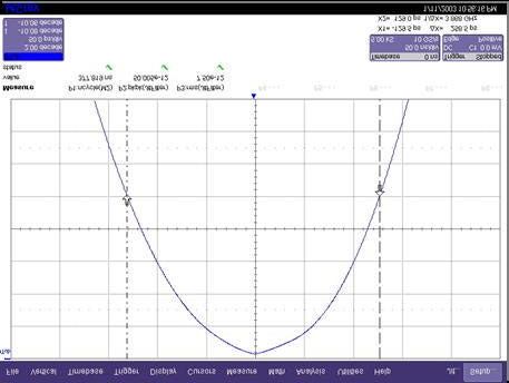
Table 1. Measurements available in SDA, ASDA, and SDM.

                        Available Measurements

    Single-Signal Measurements           SDA     SDA w/   SDM
                                          std.   ASDA     option

                  Data stream

Mask test w/ golden PLL                   X        X           X

Mask violation locator                             X
Jitter Rj , Dj, Tj, ISI, DCD (DDj), Pj    X        X

Filtered jitter                                    X

ISI plot                                           X
N-cycle vs. N plot                                 X

Bit error test with error map                      X

N-cycle jitter (data)                     X        X

      Eye pattern measurements

Eye height                                X        X           X
Eye width                                 X        X           X
Extinction ratio                          X        X           X
Eye amplitude                             X        X           X
Eye crossing point                        X        X           X
Q factor                                  X        X           X
TIE@lvl measures the time interval error of the crossing points of the
                    signal under test. SDM also includes a “golden PLL” clock recovery
                    module, which is used for forming the eye pattern without an external
                    trigger. Standard masks are included with option SDM, as indicated in
                    Table 1. Note that not all data rates can be tested with all scope models.
                    The analog bandwidth of the scope limits the upper data rate that can be
                    tested.

ASDA Capabilities   ASDA adds several key capabilities to the SDA. In its standard form,
                    the SDA includes eye pattern testing with mask hit indication, Jitter
                    testing (including jitter “bathtub” computation), and separation of jitter
                    into its random and deterministic components. It also provides a
                    breakdown of deterministic jitter into periodic, data dependent, and duty
                    cycle distortion measurements. ASDA adds the following analysis
                    features.

                       • Mask violation location –lists and displays the individual bits that
                         violate the selected mask.

                       • Filtered jitter – processes the time interval error trend vs. time with
                         a user selectable band-pass filter. This feature provides peak-to-
                         peak and rms measurements of the jitter on the filtered waveform.

                       • ISI plot – generates an eye diagram that includes only those effects
                         from data dependent sources. You can select from 3 to 7 bit
                         patterns for this test and can view the contribution from any
                         individual pattern.

                       • N-cycle vs. N plot – displays a plot of the average or peak-topeak
                         jitter over the entire acquired waveform for selected bit spacing.
                         The user selects the beginning and ending bit spacing, as well as
                         the step size. The plot shows jitter as a function of bit spacing.

                       • Bit error test with error map – measures the number of bit errors
                         and error rate on the acquired waveform by converting the wave
                         shape to a bit stream and comparing the result to a userdefinable
                         reference pattern. The data can be further divided into frames that
                         can be arranged in a 3-dimensional map with frame number on the
                         Y-axis, bit number on the X-axis, and failed bits shown in a light
                         color.
Table 2. Testing Modes Required
            Table 2. Testing Modes Required

     Standard                             Mode

   1000Base-CX                TX normalized/absolute, RX

   1000Base-LX                             TX

   1000Base-SX                             TX

   10GBase-LX4                       TX normalized

                           Transmitter, receiver low, receiver
       DVI                 high, cable test low, cable test
                           high

  FC2125, FC1063                     TX normalized

                              TX normalized, TX absolute,
FC531, FC266, FC133
                                      Receiver

                           400 beta TP2 absolute, 400 beta
    IEEE1394b
                           TP2 normalized, 400 beta receive

Infiniband 2.5 Gb/s                    Transmitter

                           OC-1, OC-3, OC-12, OC-48, STS-1
     SONET                 eye, STS-3 transmit, STS-3
                           interface

       SDH                      STM-1, STM-4, STM-16

                           TX transition, TX de-emphasized,
   PCI-Express
                           RX

Serial ATA 1.5Gb/s            TX connector, RX connector

      USB2.0

      XAUI                        Driver far, Driver near
Getting Started
Accessing SDA
To start the special SDA measurements, selectSerial Data from the
analysis menu. Alternatively, you can press theSDA button on the front
panel.
The SDA main dialog shown below will be displayed at the bottom of
the screen. The buttons on the left control the display of specific
measurements:
• Scope returns the scope to normal operation.
• Mask Test starts the eye pattern test mode.
• Jitter displays the jitter measurement screens.
• Clock allows you to designate a signal an actual clock (as opposed
to serial data) and displays a bathtub curve, TIE histogram, and Rj,
Dj, and Tj.
• BER starts the bit error rate test and displays an error map.
• Summary enters a display mode that shows jitter, mask testing,
and signal parameters in one screen.
The signal must first be set up before you enter into any test mode.
Select the source inData Source and the clock in Clock Source. These
can be, and in most cases are, the same. The selections can be active
channels as well as math or memory traces.If you do not check the Recover clock from data checkbox, it tells the
processing software that the signal should be treated as a clock; that is,
one cycle or unit interval is from rising edge to rising edge. This
contrasts with the normal selection where a data bit or UI is defined
from edge to edge, regardless of whether they are rising or falling. The
Signal Type control determines the data rate and mask for eye pattern
and jitter tests. Signal Frequency indicates the data rate for the selected
standard, which you can set when Custom is selected as the signal type.
And Signal Mode allows the selection of specific modes (such as
Transmitter or Receiver), depending on the selected signal type. For
example, some standards define separate transmit and receive masks.
The PLL section at the right of the dialog consists of two interlocked
controls: one for the Cutoff Divisor and the other for the PLL Fre-
quency. The cutoff divisor is the number by which the data rate is
divided to determine the PLL loop bandwidth filter. This bandwidth can
also be set directly using the PLL frequency control.
The default value for the cutoff divisor is 1667, which is the defined
value for a golden PLL. The PLL recovers a clock from the channel
selected in the Data Source control and uses this as a reference clock
for jitter (TIE) measurement, eye pattern generation, and bit error
testing. The PLL On checkbox, when left unchecked, disables the PLL
and reverts to a reference clock that operates at a fixed rate equal to the
value in the Signal Frequency control. Find Frequency causes the
instrument to search for the actual frequency of the signal in case it
differs from the specified value. The resulting frequency from this
search is displayed in the Signal Frequency control.
SDA Acquisition The SDA measures eye pattern and jitter parameters by processing a
Settings long record in order to recover the clock and to measure the jitter
statistics. This same record is also divided into segments, using the
recovered clock to form the eye pattern. The record length and sample
rate have a dramatic impact on the accuracy of these measurements.
The sampling rate sets the time resolution for both the clock recovery
and jitter measurements, while the record length allows for PLL settling
and statistical accuracy. It is important that the sampling rate be set to
its maximum value for the best performance. This value is 20 Gs/s for
all standards with rise times faster than 300 ps. A minimum of 3000 data
edges is required for PLL settling in all cases. So for a signal consisting
of 12 samples per bit, for example, a minimum record length of 50k
samples is needed. In practice, 400k samples is the minimum practical
record size to produce acceptable results.Theory of operation
The SDA operates by processing a long signal acquisition. Processes
include clock recovery, eye pattern computation, jitter measurement,
and bit error testing ? all performed on the same data record. The
processes will be described in detail in this section.
Clock Recovery An accurate reference clock is central to all of the measurements
performed by the SDA. The recovered clock is defined by the locations
of its crossing points in time. Starting with zero, the clock edges are
computed at specific time intervals relative to each other. A 2.5 GHz
clock, for example, will have edges separated in time by 400 ps. The
first step in creating a clock signal is the creation of a digital phase
detector.
This is simply a software component that measures the location in time
at which the signal crosses a given threshold value. Given the maximum
sampling rate available, 20 GHz, interpolation is necessary in most
cases. Interpolation is automatically performed in the SDA when three
or fewer samples exist on any given edge. Interpolation is not performed
on the entire waveform. Rather, only the points surrounding the
threshold crossing are interpolated for the measurement. To find the
crossing point, a cubic interpolation is used, followed by a linear fit to
the interpolated data. This is shown in Figure 1.
threshold
1. locate points bracketing threshold
2. add new "cubicly" interpolated points
3. estimate TOC "linearly"
time of
crossing
estimate
Figure 1. SDA Threshold Crossing AlgorithmThe clock recovery implementation in the SDA is shown in Figure 2.
The algorithm generates time values corresponding to a clock at the data
rate. The computation follows variations in the data stream being tested
through the use of a feedback control loop that corrects each period of
the clock by adding a portion of the error between the recovered clock
edge and the nearest data edge.
(addition)
Base Period (addition)
(constant numeric
value)
Digital
(numeric)
output values
(subtraction)
Data Digital Phase
sequence Detector Digital
input Filter Multiplier
(IIR) Memorized
previous result
Figure 2. SDA Clock Recovery Algorithm
In Figure 2, the initial value of the output and the digital phase detector
are set to zero. The next time value output is equal to the nominal data
rate. This value is fed back to the comparator on the far left, which
compares this time value to the measured time of the next data edge
from the digital phase detector. The difference is the error between the
data rate and the recovered clock. This difference is filtered and added
to the initial base period to generate the corrected clock period. The
filter controls the rate of this correction by scaling the amount of error
that is fed back to the clock period computation. This filter is imple-
mented in the SDA as a single-pole infinite impulse response (IIR) low-
pass filter, whose equation is:
1 1
yk = x k + 1 − y k −1
n n
The value of yk is the correction value for the kth iteration of the
computation, and xk is the error between the kth data edge and the
corresponding clock edge. Note that the current correction factor is
equal to the weighted sum of the current error and all previous
correction values. The multiplier value is set to 1 in the SDA. The value
of n is the PLL cutoff divisor that is set from the SDA main dialog. The
cutoff frequency is Fd/n where Fd is the data rate. This filter is relatedto its analog counterpart through a design process known as impulse
invariance and is only valid for cutoff frequencies much lower than the
data rate. For this reason, the minimum PLL cutoff divisor setting is 20
in the SDA.
The factor n determines the number of previous values of the correction
value y that are used in the computation of the current correction value.
This is theoretically infinite; however, practically there is a limit to the
number of past values included. One can define a “sliding window”
equivalent to a number of UI of the data signal for a given value of n.
This is useful for measuring signals such as serial ATA and PCIExpress
where the specifications call for clock recovery over a finite window.
The equivalent bandwidth of the sliding window is given by a sin(x)/x
function. The first null of this function occurs at x = π or 1/2 the bit rate
(the digital equivalent of the frequency of a signal at the sampling rate
is 2π and the sampling rate for clock recovery is the data rate). This is
scaled by the window size to be 2π/N where N is the window in UI. The
3 dB point of the sin(x)/x function is at 0.6π/N or 0.3Fd/N for a window
length of N. This gives us a relationship between N and n:
Fd/n = 0.3Fd/N or n = N/0.3
For a sliding window size of 250, the equivalent value of n would be 833.
Eye Pattern An eye diagram shows all values that a digital signal takes on during a bit
Measurement period. A bit period or UI (unit interval) is defined by the data clock so
some sort of data clock is needed in order to measure the eye pattern. The
traditional method of generating an eye pattern involves acquiring data on
an oscilloscope using the data clock as a trigger. One or more samples are
taken on each trigger. The samples are stored in a persistence map with
the vertical dimension equal to the signal level and the horizontal position
equal to the sample position relative to the trigger (or data clock). As
many data points are collected, the eye pattern fills in with multiple
occurrences of time and amplitude values counted by incrementing
counters in each x,y “bin.” Timing jitter is indicated by the horizontal
distribution of the points around the data crossings. The histogram of the
bins around the crossing points gives the distribution of jitter amplitude.
A recovered clock is used if there is no access to a data clock. The
recovered clock is normally a hardware PLL designed to operate at
specific data rates and with a cutoff frequency of Fd/1667. One of the
major drawbacks of a hardware clock recovery circuit is that jitter
Histogram of Zero Crossing in Eye Pattern
associated with the trigger circuit adds to the measured jitter by creating
Showing Jitter Distribution
uncertainty in the horizontal positioning of the eye pattern samples.The SDA measures eye patterns without using a tirgger. It does this by
using the software clock recovery discussed above to divide the data
record into segments along the time values of the clock. For the
purposes of dividing the time line into segments, the time resolution in
the waveform record is infinite. The samples occur at fixed intervals of
50 ps/pt (for a 20 Gs/s sampling rate). The samples are positioned
relative to the recovered clock timing points and the segments delimited
by the clock samples are overlayed by aligning the clock samples for
each segment. A monochrome or color persistence display is used to
show the distributon of the eye pattern data. Jitter added by the measure-
ment system in this case is from the sampling clock, which, for the
SDA, is very low: on the order of 1 ps rms.
Eye Violation The eye pattern is measured by overlaying segments of a continuous
Locator (ASDA) acquisition. Since the complete data record is available, the location of
individual bits can be determined by comparing each bit interval in the
original waveform with the selected mask. The mask is aligned hori-
zontally along the mean bit interval, and vertically along the mean one
and zero level in the case of a relative mask. Absolute masks exist for
some standards and are defined in the vertical dimension by specific
voltage values. Figure 3 below shows this alignment. When mask testing
is turned on, the entire waveform is scanned bit-by-bit and compared to
the mask. When a mask hit is detected, the bit number is stored and a
table of bit values is generated. This table is numbered, starting with the
first bit in the waveform, and can be used to index back to the original
waveform to display the waveform of the failed bit.
center on eye
amplitude or
absolute voltage
levels for
absolute masks
centered on mean bit rate
Figure 3. Eye Mask Alignment for Violation LocatorEye Pattern There are several important measurements that are made on eye
patterns. These are specified as required tests for many standards. Eye
Measurements
measurements mainly deal with amplitude and timing, which are
described next.
Eye Amplitude Eye amplitude is a measure of the amplitude of the data signal. The
measurement is made using the distribution of amplitude values in a
region near the center of the eye (normally 20% of the distance between
the zero crossing times). The simple mean of the distribution around the
‘0’ level is subtracted from the mean of the distribution around the ‘1’
level. This difference is expressed in units of the signal amplitude
(normally voltage).
Eye Height The eye height is a measure of the signal to noise of a signal. The mean
of the ‘0’ level is subtracted from the mean of the ‘1’ level as in the eye
amplitude measurement. This number is modified by subtracting the
standard deviation of both the ‘1’ and ‘0’ levels. The measurement
basically gives an indication of the eye opening.
Eye Width This measurement gives an indication of the total jitter in the signal. The
time between the crossing points is computed by measuring the mean of
the histograms at the two zero crossings in the signal. The standard
deviation of each distribution is subtracted from the difference between
these two means.
Extinction Ratio This measurement, defined only for optical signals, is the ratio of the
optical power with the laser in the on state to that of the laser in the off
state. Laser transmitters are never fully shut off because a relatively long
period of time is required to turn the laser back on thus limiting the rate
at which the laser can operate. The extinction ratio is the ratio of two
power levels, one very near zero, and its accuracy is greatly affected by
any offset in the input of the measurement system. Optical signals are
measured using optical to electrical converters on the front end of the
SDA. Any DC offset in the O/E must be removed prior to measuring the
extinction ratio. This procedure is known as dark calibration. The output
Eye amplitude of the O/E is measured with no signal attached (i.e., dark) and this value
Eye height is subtracted from all subsequent measurements.
Eye width
Eye Crossing Eye crossing is the point at which the transitions from 0
to 1 and from 1 to 0 reach the same amplitude. This is the point on the
eye diagram where the rising and falling edges intersect. The eye
crossing is expressed as a percentage of the total eye amplitude. The eye
crossing level is measured by finding the minimum histogram width of
a slice taken across the eye diagram in the horizontal direction as the
vertical displacement of this slice is varied.Average Power The average power is a measurement of the mean value of all levels that
the data stream contains. It can be viewed as the mean of a histogram of
a vertical slice through the waveform, covering an entire bit interval.
Unlike the eye amplitude measurement, where we separate the ones and
zeroes histograms, the average power is the mean of both histograms.
Depending on the data coding that is used, the average power can be
affected by the data pattern. A higher density of ones, for example, will
result in a higher average power. Most coding schemes are designed to
maintain an even ones density resulting in an average power that is 50%
of the overall eye amplitude.
Q factor or BER The Q factor measures the overall signal-to-noise ratio of the data
signal. It is computed by taking the eye amplitude and dividing it by the
sum of the standard deviations of the zero and one levels. All of these
measurements are taken in the center (usually 20%) of the eye.
Jitter measurement The SDA measures jitter by evaluating the time difference between the
data crossing points and those of an ideal reference clock. The reference
clock used for jitter measurements in the SDA is the software PLL
described above. This approach provides an almost ideal reference
because the software clock adds no jitter to the signal beyond the very
small contribution from the sampling clock. Software implementation
allows very tight control over the clock bandwidth while at the same
time allowing a great deal of flexibility.
TIE measurement Time interval error or TIE is a measurement of the time error between
edges of a data (or clock) signal and those from an ideal, jitter-less clock
(Figure 4).
TIE TIE TIE TIE
Figure 4. TIE Measurement between Data (above)
and Ideal Clock (below)The clock can be a separate reference or, more commonly, a recovered
clock from the data stream. A recovered clock allows control of con-
tributions to the overall jitter from components at lower rates. The
widely used “Golden PLL” from the Fibre Channel specification has a
loop cutoff frequency of the data rate/1667. This PLL has the effect of
limiting the contribution of jitter components at low rates to the overall
jitter value by enabling the recovered clock to track slow variations in
the data rate. Implementation of the PLL in the SDA allows adjustment
of the cutoff factor (1667 in the Golden PLL) from 20 to 10,000, giving
excellent control of the contributions of jitter at specific rates. Clock
recovery and TIE measurement in the SDA are performed on con-
TIE Histogram secutive edges in a single, long acquisition.
The TIE values measured from the data signal are collected into a
histogram of TIE value vs. the number of occurrences of that value. This
histogram is computed over the complete set of measurements in a
given acquisition, and is updated on each subsequent acquisition so that
the histogram is the cumulative result of all acquisitions from the last
reset. The main object of measuring the histogram of TIE is to determine
the likelihood of a jitter value exceeding a given maximum. Systems
typically specify bit error rates in the 10-12 range. When performing
jitter measurements, one is interested in determining the probability that
a data transition occurs at the same time that the data is being sampled
by the detector. This results in the conditional probability of a data edge
occurring at a given time within a bit period, given that the data is
sampled at that time. This relationship is shown graphically in the
bathtub curve which will be discussed shortly.
In order to measure events with probabilities on the order of 10-12, a
sufficient number of edges must be sampled to determine the likelihood
of such an event. It is not practical with any sort of instrument to directly
measure the jitter histogram to this level, so the histogram is
extrapolated from a smaller set of measurements. The jitter histogram is
a complex combination of sources that are bounded (deterministic) and
random. Bounded components have a specific range of values that is
limited and does not grow with sample size. That is, these bounded
components do not grow as they are observed over longer and longer
time spans. Random jitter components, on the other hand, are Gaussian
Top: TIE Histogram,
in nature and grow without bound as the observation time increases. The
Bottom: Log of TIE Histogram
(red) and Extrapolated Tails (blue)
goal of extrapolating the jitter histogram is to observe the signal long
enough so that the deterministic components are completely characterized
and the extremes of the histogram are Gaussian. Once the histogram is
measured, the logarithm of the distribution is taken. The Gaussian tails ofthis curve will have a quadratic shape (log(exp(x2)) = x2). A least squares
fit of a quadratic curve is then made to each tail of the log-scaled
histogram. The resulting composite curve is the equivalent histogram
for a very long observation (up to 1016 bits). This histogram represents
the complete probability distribution function (PDF) of TIE.
The object of this measurement is to determine the probability of a data
transition occurring at a particular time, given that the data is sampled
at that time. The PDF of TIE is centered at a zero crossing of the data,
and its mean is at the ideal zero crossing. The probability of a data
crossing occurring at any time is 1 so the integral of the PDF from
negative to positive infinity is 1. Suppose we wish to find the probability
of an edge occurring at x ps, or more, to the right of the crossing point.
This value can be found by integrating the PDF from infinity to x. This
is the probability that an edge will occur at our sampling point if we
sample at x. This probability is, of course, also the probability of a bit
bit interval error occurring if the data is sampled at point x. The concepts of
probability of a certain jitter value occurring and bit error rate are
directly related. By integrating the PDF of TIE for all values of offset,
PDF (histogram) the CDF (total jitter curve) is created. The total jitter curve is also
of timing jitter
centered at the zero crossing of the data. The probability of a given jitter
value to the right of the crossing is given by the values on the right-hand
probability of X>x side of the curve, while probabilities on the left are given by the left-
x
hand side of the curve.
The data stream consists of a large number of consecutive bits, and the
The Bathtub Curve jitter distribution applies to any transition in the data stream. One can
look at the left-hand side of the total jitter curve as the probability of an
edge occurring before the given transition or, equivalently, as the
probability that an edge will occur before the next transition. By
Decreasing BER arranging the total jitter curve in this way, we arrive at the bathtub curve.
The bathtub curve offers an excellent way to view the relationship
between bit error rate and jitter. The sides of the bathtub give the bit
error rate for any given sampling point within a bit interval. The
horizontal distance between the curves at a given vertical displacement
Offset from zero crossing->
or bit error rate gives the eye opening at that BER. As long as the sides
of the curve do not touch, there is a sampling point at which the desired
bit error rate can be achieved.
The total jitter is simply the width of the total jitter curve. Note that the
total jitter curve becomes wider as bit error rate becomes lower (Figure 5):Total Jitter, Rj,
and Dj
Figure 5. Random and deterministic jitter
For this reason, the bit error rate must be specified when referring to
total jitter. The total jitter is a function of the measured and extrapolated
histogram of TIE, and is well understood and can be accurately
measured using a number of techniques. The separation of random and
deterministic jitter is less well defined, however. There are several
techniques employed for separating random and deterministic jitter
from total jitter. The SDA uses the effective Dj model defined in the
Fibre Channel specification (Figure 5) and is also used in the BERt scan
method. Deterministic jitter, as defined in this standard and adopted by
other standards that require Dj measurements, is based on the model:
Tj = αRj + Dj
The Dj parameter is the separation between the two Gaussian distributions
that are used to fit the tails of the histogram. The above equation gives a
method for relating total jitter to its random and deterministic
components. The total jitter curve gives the total jitter as a function of bit
error rate. The width of this curve at any given vertical displacement or bit
error rate is the total jitter for that BER. The random jitter is Gaussian in
nature, so its distribution is completely defined by the mean and standard
deviation. The mean values of the two Gaussians are separated by the
value of Dj as defined in the above equation and in Figure 5. The standard
deviation is the value Rj, which is assumed to be the same for both tails.
The value a is the number of standard deviations from the mean of a
Gaussian distribution corresponding to the selected bit error rate or,
equivalently, where the probability is less than the BER. The values of α
are well known, so finding Rj and Dj is a matter of solving the total jitter
equation for these two values. We need a minimum of two Tj values to do
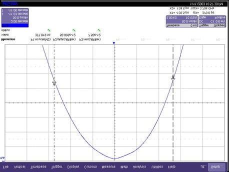
this , but we have many available in the total jitter curve. Figure 6 shows
an example using two measurements of Tj. We have
258.5 = 12.7Rj + DEj
270 = 13.4Rj + Djwhich gives Rj = 16.43 ps and Dj = 49.86 ps. This computation is
performed by the SDA for many values of Tj from bit error rates of 10-10
down to 10-16. The average of all the computed Rj and Dj values is the
final result displayed on the instrument.
Figure 6.Components of Dj Deterministic jitter is caused by a number of systematic effects. Jitter
can be periodic so that it appears as a sine save or some other repeating
shape. It can also come from data pattern dependent sources. The former
is often referred to as periodic jitter (Pj), while the latter is called Data
Dependent Jitter (DDj) or Intersymbol Interference (ISI). A third source
of deterministic jitter is known as Duty Cycle Distortion (DCD), a
measure of the pulse width difference between a logical 1 and 0. There
is also a fourth source known as bounded, uncorrelated jitter, which is
from other sources not related to the data rate or pattern.
Periodic Jitter Periodic jitter is the repetitive variation of the data rate (or bit interval)
over time. Its sources are often related to instabilities in reference clocks
or power supply harmonics. In some cases, the data rate is varied at a
specific rate and amplitude in order to spread the clock energy. This is
known as spread spectrum clocking. While the SDA reports Dj by
analyzing the overall jitter distribution, periodic jitter is measured by
looking at the jitter in the frequency domain through the use of an FFT.
The Fourier transform is taken of the trend of the time interval error
measurements, and the spectrum is evaluated to determine the presence
of periodic jitter.
Since the time interval error is measured for each bit transition, the
maximum frequency that can be seen in its spectrum is 1/2 the data rate
(this is the equivalent of the Nyquist rate). There may be spectral lines
at the repetition rate of the data pattern if the data contains a repeating
pattern. Spectral components at these points are ignored by the Pj
algorithm in the SDA. You must enter the pattern length on the SDA
jitter dialog to ensure that the software will recognize the data pattern in
the jitter. An adaptive threshold is applied to the spectrum, and the level
of all spectral components above this line (except for those at the pattern
repetition rate) are added together to compute the total periodic jitter.
Data Dependent This type of jitter is the result of differences in the propagation time
Jitter (or ISI) through the transmission medium among different data patterns. A
simple example is a transmission medium that acts as a low-pass filter.
To simplify this example, let us assume that the 3 dB cutoff frequency
is at the bit rate. A data pattern consisting of repeating 1 and 0 values
(1010101….) will have a strong component at the bit rate and, passing
through the filter, it will be attenuated and possibly phase shifted as
well. Another pattern with fewer transitions (11001100…) will have
more energy at a lower frequency, and will have very little attenuation
and no phase shift. The lower signal level out of the channel for the first
pattern will tend to shift the crossing point, since the position of the
slope of the transitions is shifted. Any phase shift will also add to this.The second pattern, of course, is unaffected by the filter and so it
propagates through the system without distortion. The time difference
between the two crossing points is data dependent jitter.
The SDA measures DDj directly on the acquired waveform and does not
use the statistics computed for the Tj measurement. The measurement
uses a long acquisition of bits and searches the waveform for patterns of
a selected length. This length is variable from 3 to 7 bits. Once a pattern
length is selected, the waveform is searched for all combinations of bits
in a pattern of that length. For example, if a 5 bit pattern is selected, the
waveform is searched for all 32 different bit patterns that the 5 bits can
DDj caused by low-pass filter.
Note the slow rise time induced by
have. The recovered clock gives a timing reference for the bits in the
the low-pass filter waveform so that we know exactly where to sample the waveform to
determine its bit value. The waveform is scanned 5 bits at a time in this
example, and the 5-bit window is stepped in one-bit increments for each
comparison. The waveforms for bit patterns of the same value are
averaged together.
At the completion of the measurement in our 5-bit example, there are 32
averaged 5-bit-long waveforms. The averaging removes all random
noise and jitter, as well as periodic components of jitter. These wave-
forms are overlaid by lining up the first bit and viewing the transition to
the last bit. An eye diagram is presented on the display, which is
centered around the 4th bit. The DDj parameter displays the width of the
zero crossing at the right of this eye pattern.
Duty Cycle Duty cycle distortion is a measure of the difference between the pulse
Distortion width of a 1 level and that of a 0 level. This measurement, like all of the
other measurements of Dj components, is measured directly on the
captured waveform in the SDA. Duty cycle distortion is measured as the
width at the 50% amplitude of the positive-to-negative transitions and
the negative-to-positive transitions.
This measurement is unique in that it is always taken at the 50% level
while all of the other measurements including time interval error are
measured at a user-selected level, which can be set at the true crossing
point. For signals with crossing points significantly different from 50%,
one can observe high DCD while at the same time measuring little or no
deterministic jitter (Dj). This occurs when the crossing point for jitter
measurements is set to the data crossing point. This is valid since
measuring duty cycle distortion at the crossing point will always give a
value of zero. Therefore, it is meaningless to measure DCD at the
crossing point.Bit Error Rate The SDA measures bit error rate directly on the captured bit stream by
using the recovered clock to sample the waveform and a user-selectable
threshold. The data are assumed to be NRZ, so a high level is interpreted
as a ‘1’ and a low level is interpreted as a ‘0.’ The bit stream that is
decoded in this process is compared bit-by-bit with a userdefined known
pattern. Since the instrument does not have any information as to which
bit in the pattern it has received, a searching algorithm is used to shift
the known pattern along the received data until a match is found.
A match is determined when more than half of the bits are correct for a
given shift of the known pattern. No match can be found if the bit error
rate is over 50% or if the wrong pattern is selected. In this case, the bit
error rate will indicate 0.5, meaning that exactly 1/2 of the bits are in
error, which, of course, is the worst case.
Bit Error Map A further level of debugging is available through the bit error map. This
display is a view of the bit errors in the data stream relative to any
framing that may be present in the signal. There are several options for
framing that may be set. The general form of the data signal is shown
below.
hdr payload hdr payload
The header portion is a fixed pattern that can be set to any p attern. The
header must be one or more bytes if it is present. The software searches
for the header if present and treats the bits between headers as a frame.
Each frame is displayed as a line of pixels in an x-y map, and each
successive frame is displayed below the previous one in a raster fashion.
Bit errors are computed only on the payload sections of the hdr payload
hdr payload data stream. Framing can also be defined by a specific
number of bits without a header.
An example of this is a pseudorandom bit sequence (PRBS) of a specific
length, 127 bits for example. In this case, setting the frame size to 127
will display one repetition of this sequence per line of the error map. Bit
errors are displayed as a lighter color whereas non-errored bits are
shown in a dark blue color. By displaying bit errors on a frame by frame
basis, pattern dependent errors can be clearly seen as lightly colored
vertical lines in the error map. Refer to Figure 7 and Figure 8.Figure 7. Bit Error Map for 127-bit Pattern Containing Random Errors (White Squares) Figure 8. Bit Error Map for 127 Bit Pattern Containing Pattern Dependent Errors
Operator’s Reference

Main SDA Dialog   Enter the main SDA setup dialog by selecting Serial Data from the
                  Analysis menu or by pressing the SERIAL DATA button on the SDA front
                  panel. You can also access this dialog by touching any descriptor label
                  associated with an SDA measurement.

SCOPE             This button enters the scope mode; that is, it disables all SDA
                  measurements. Any waveforms that were shut off when the SDA mode
                  was entered will be redisplayed upon pressing the scope button.

MASK TEST         Displays the eye pattern of the signal under test along with any selected
                  mask. The dialog changes to the Mask Test dialog. Any selected mask
                  measurements will also be displayed as parameters below the waveform
                  grid.

JITTER            Enters the jitter test mode and displays the Jitter dialog. Selected jitter
                  measurements may also appear below the grid.

BER               Displays the bit error test screen and dialog.

CLOCK             Enables you to designate an input to be an actual clock, as opposed to a
                  serial data stream. This mode of operation produces a bathtub curve,
                  TIE histogram, and key clock parameter measurements Tj, Rj, and Dj.

SUMMARY           Displays the summary screen, which includes eye pattern, jitter bathtub,
                  jitter histogram, and amplitude histogram along with Tj, Rj, Dj and
                  rise/fall time.

Data Source       This control lets you define the signal to be tested. The signal can be any
                  channel or math trace. For example, when testing differential signals , it
                  is often desired to measure the true differential crossing point. This can
                  be done by forming a math trace that is one channel minus another.

Clock Source      This channel is processed by the software clock recovery algorithm in
                  the SDA to provide the reference clock for all measurements. This can
                  be the same as the data channel or a separate signal.
Signal Frequency The signal frequency (bit rate) is the symbol transmission rate of the
signal under test. This value is set by the selected signal type, or you can
manually set it to any value when Custom is selected as the standard.
The value in this control represents the start frequency for the software
clock recovery. If it is significantly different from the actual data rate,
the recovered clock may not converge.
Find Frequency Find frequency measures the average bit rate across the entire acquired
waveform. This control can be used to adjust the initial estimate of the
PLL frequency for signals that are not operating exactly at the specified
bit rate. It is also a useful way to use standard masks with non-standard
bit rates.
PLL Cutoff Divisor This sets the PLL loop bandwidth as a ratio of the bit rate. The default
value is 1667, which is the standard value for the so-called “Golden
PLL,” as defined in the Fibre Channel standard. This value is variable
from 20 to 10,000 to allow other loop bandwidths to be used.
PLL Frequency This control displays the cutoff frequency of the PLL. It is locked to the
PLL cutoff divisor, and changes along with that value. You can select
either the frequency or the divisor.
PLL On The PLL On checkbox allows measurements to be made without the
PLL being engaged. When this box is left unchecked, the average data
rate is used for all timing measurements.
Mask Test
The Mask Test dialog controls eye pattern tests with the SDA. From this
dialog, you can select measurements and parameters for performing eye
Eye Mode pattern tests.
Eye mode sets the method used for creating the eye pattern. The two
choices are Traditional and Sequential. Traditional mode uses an ex-
ternal clock to position the waveform samples on the display in the same
way that an oscilloscope uses external triggering to build an eye pattern.
Sequential mode uses the software clock recovery to divide the wave-
form into bit sized samples to create the eye pattern. This is described in
more detail in the preceding Theory section. The clock for either mode
is the channel selected in the Clock Source control in the SDA main
dialog.Eye Persistence Persistence can be viewed in color-graded or gray scale mode. The
color-graded scale shows less frequent occurrences in blue and more
frequent ones in white. The monochrome setting shows the frequency of
occurrence in the degrees of intensity.
User Signal This can be any channel or math function in the instrument. The selected
channel is captured synchronously with the signal under test, selected in
the Data Source control in the main dialog. This signal is displayed in
the mask violation locator screen, using the same time scale as the
waveform displaying the mask violations. The correlated view allows
diagnosis of mask failures caused by interfering signals.
Mask Margins These controls allow you to increase the size of the “illegal” areas of the
mask by the specified percentage, in either the X or Y dimension. Mask
margins allow testing of signals to tighter standards, and the separate x
and y controls enable independent specification of jitter and noise
margins.
Vertical Auto Fit Checking this box causes the instrument to scale the eye pattern to fit
the mask in the vertical dimension by centering the mean 1 and 0 values
between the respective mask polygons. Auto fit is available for all signal
types; however, it is unchecked by default for those masks that are
defined as absolute. Absolute masks are defined in terms of voltage on
the vertical axis and the absolute value of the waveform amplitude.
Checking this box, when using absolute masks, will result in
measurements that are invalid for the given standard. There are cases
when the mask may seem to disappear in the case of waveforms that are
grossly offset from the specified value. This is normal operation, since
absolute masks are positioned by their voltage values.
Clock Setup The software clock recovery system in the SDA operates by detecting
threshold crossings. The threshold type control allows you to set this
threshold as either absolute (in volts) or relative (as a percentage of the
p-p signal). The slope control determines the slope of the first zero
crossing that is used for clock recovery. If Positive is selected, clock
recovery begins with the first rising edge in the data, while Negative
slope will start with the first falling edge. The Percent Level control is
used to set either the absolute or percentage level of the threshold.
Testing Checking this box enables mask testing. Testing is performed on each
bit in the waveform. Violations are indicated by red circles in the eye
pattern display.You can also read