Continuous Real-World Inputs Can Open Up Alternative Accelerator Designs
←
→
Page content transcription
If your browser does not render page correctly, please read the page content below
Continuous Real-World Inputs
                   Can Open Up Alternative Accelerator Designs

     Bilel Belhadj†                  Antoine Joubert†                         Zheng Li§                 Rodolphe Héliot†               Olivier Temam§
                                                   †
                                                       CEA LETI, France              §
                                                                                         INRIA, Saclay, France

ABSTRACT                                                                                   cessing tasks. Examples include voice recognition which has re-
Motivated by energy constraints, future heterogeneous multi-cores                          cently become mainstream on smartphones (e.g., Siri on iPhones),
may contain a variety of accelerators, each targeting a subset of the                      an increasing number of cameras which integrate facial expression
application spectrum. Beyond energy, the growing number of faults                          recognition (e.g., photo is taken when a smile is detected), or even
steers accelerator research towards fault-tolerant accelerators.                           self-driving cars which require fast video and navigation process-
   In this article, we investigate a fault-tolerant and energy-efficient                   ing (e.g., Google cars), and a host of novel applications stemming
accelerator for signal processing applications. We depart from tra-                        from and based upon sensors such as the Microsoft Kinect, etc.
ditional designs by introducing an accelerator which relies on unary                       These devices and applications may well drive the creation of less
coding, a concept which is well adapted to the continuous real-                            flexible but highly efficient micro-architectures in the future. At
world inputs of signal processing applications. Unary coding en-                           the very least, they already, or may soon correspond, to applica-
ables a number of atypical micro-architecture choices which bring                          tions with high enough volume to justify the introduction of related
down area cost and energy; moreover, unary coding provides grace-                          accelerators in multi-core chips.
ful output degradation as the amount of transient faults increases.                           A notable common feature of many of these emerging appli-
   We introduce a configurable hybrid digital/analog micro-archi-                          cations is that they continuously process “real-world”, and often
tecture capable of implementing a broad set of signal processing                           noisy, low-frequency, input data (e.g., image, video, audio and some
applications based on these concepts, together with a back-end op-                         of the radio signals), and they perform more or less sophisticated
timizer which takes advantage of the special nature of these appli-                        tasks on them. In other words, many of these tasks can be deemed
cations. For a set of five signal applications, we explore the differ-                     signal processing tasks at large, where the signal nature can vary.
ent design tradeoffs and obtain an accelerator with an area cost of                        Digital Signal Processors (DSPs) have been specifically designed
1.63mm2 . On average, this accelerator requires only 2.3% of the                           to cope with such inputs. Today, while DSPs still retain some spe-
energy of an Atom-like core to implement similar tasks. We then                            cific features (e.g., VLIW, DMA), they have become increasingly
evaluate the accelerator resilience to transient faults, and its ability                   similar to full-fledged processors. For instance the TI C6000 [1]
to trade accuracy for energy savings.                                                      has a clock frequency of 1.2GHz, a rich instruction set and a cache
                                                                                           hierarchy.
                                                                                              The rationale for this article is that continuous real-world input
1.     INTRODUCTION                                                                        data processing entails specific properties which can be leveraged
   Due to ever stringent technology constraints, especially energy                         to better cope with the combined evolution of technology and ap-
[12] and faults [6], the micro-architecture community has been con-                        plications. We particularly seek low-cost solutions to enable their
templating increasingly varied approaches [42, 15, 37] for design-                         broad adoption in many devices, enough flexibility to accommo-
ing architectures which realize different tradeoffs between appli-                         date a broad set of signal processing tasks, high tolerance to tran-
cation flexibility, area cost, energy efficiency and fault tolerance.                      sient faults, and low-energy solutions.
Finding appropriate accelerators is both an open question and fast                            The starting point of our approach is to rely on unary coding
becoming one of the key challenges of our community [36].                                  for representing input data and any data circulating within the ar-
   But in addition to technology constraints, there is a similarly im-                     chitecture. Unary coding means that an integer value V is coded
portant evolution in the systems these chips are used in, and the                          with a train of V pulses. This choice may come across as inef-
applications they are used for [7]. Our community is currently fo-                         ficient performance-wise, since most architectures would transmit
cused on general-purpose computing, but a large array of more or                           value V in a single cycle using log2 (V ) bits in parallel. However,
less specialized (potentially high-volume) devices and applications                        while real-world input data may be massive (e.g., high-resolution
are in increasing demand for performance and sophisticated pro-                            images/videos), its update frequency is typically very low, e.g.,
                                                                                           50/60Hz for video, and rarely above 1MHz for most signals, except
                                                                                           for high-frequency radio signals. Both the time margin provided
                                                                                           by low frequency input signal and by unary coding enable a set
Permission to make digital or hard copies of all or part of this work for                  of atypical micro-architecture design innovations, with significant
personal or classroom use is granted without fee provided that copies are                  benefits in energy and fault tolerance; some of these innovations
not made or distributed for profit or commercial advantage and that copies                 are nested, one enabling another, as explained thereafter.
bear this notice and the full citation on the first page. To copy otherwise, to               The first benefit of unary coding is more progressive tolerance
republish, to post on servers or to redistribute to lists, requires prior specific
permission and/or a fee.
                                                                                           to faults than word-based representations. Errors occurring on data
ISCA’13, Tel-Aviv, Israel.                                                                 represented using n bits can exhibit high value variations depend-
Copyright 2013 ACM 978-1-4503-2079-5/13/06 ...$15.00.
ing on the magnitude of the bit which suffered the fault (low to
high order). With unary coding, losing one pulse induces a unit er-
ror variation, so the amplitude of the error increases progressively
with the number of faults.
The ability to lose pulses with no significant impact on applica-
tion behavior brings, in turn, cost and energy benefits. Two of the
main architecture benefits are: (1) the switches in the fabric rout-
ing network can operate asynchronously, without even resorting to
handshaking, (2) the clock tree is smaller than in a usual fabric
since fewer elements operate synchronously.
Another major benefit of unary coding is the existence of a pow-
erful, but very cost effective operator, for realizing complex signal
processing tasks. Recent research has shown that most elementary
signal processing operations can not only be expressed, but also
densely implemented, using a Leaky Integrate and Fire (LIF) spik-
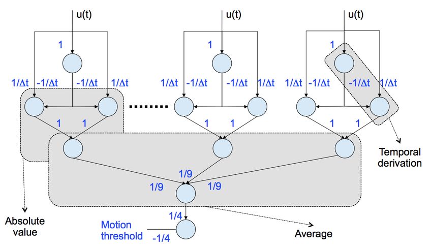
Figure 1: Neuron-based programming of motion estimation,
ing neuron [40, 29, 10]. A spiking neuron may be slower than
the main operations are highlighted, and the weights are shown
a typical digital operator but it realizes more complex operations,
on the edges.
such as integration, and the low input signal frequency provides
ample time margin. Each operator can be built with just a few
such neurons; however, to dispel any possible confusion, there is
no learning involved, the weights of the synapses are precisely set, ron) of this architecture has been successfully taped out, and the
i.e., programmed, to accomplish the desired function; the neuron is full architecture presented in this paper is in the process of being
only used as an elementary operator. taped out.
Using a spiking neuron enables, in turn, additional micro-archi- In Section 2, we recall the basic concepts allowing to program
tecture optimizations. A spiking neuron can be realized as a dig- signal processing applications as graphs of operators, and to im-
ital or analog circuit, but analog versions have been shown to be plement these operators using analog neurons. In Section 3, we
much denser and more energy efficient [20], so we select that op- present the micro-architecture and how real-world input data char-
tion. However, we avoid two of the main pitfalls of past attempts acteristics are factored in the design. In Section 4, we discuss
at designing analog architectures: the difficulty to chain and pre- the back-end generator, especially which mapping optimizations
cisely control analog operators, and the difficulty to program such help keep the architecture cost low. In Section 5, we introduce the
architectures [17]. For the first issue, we resort to a hybrid digital- methodology and applications. In Section 6, we explore the op-
analog grid-like architecture where the routing network and control timal architecture configuration (area) for our target applications,
is asynchronous but digital, while only the computational operators and evaluate the energy, fault tolerance and bandwidth of our ar-
at the grid nodes are analog. The programming issue is overcome chitecture. In Section 7, we present the related work and conclude
by creating a library of signal processing operations, themselves in Section 8.
based on the unique nature of the elementary hardware operator
(spiking neuron).
A signal processing application is then expressed as a graph of 2. PROGRAMMING
such operations and mapped onto the architecture. While such In this section, we explain the main principles that allow to ex-
graphs can theoretically require a massive number of connections, press a signal processing task as a combination of elementary oper-
unary coding enables again a set of unique back-end compiler opti- ators, themselves based upon a unique elementary analog operator
mizations which can further, and drastically, reduce the overall cost (the analog neuron). We leverage recent research on the topic [10],
of the architecture. and we briefly recap the main principles below, because they are not
Unary coding and the low input signal frequency enable addi- yet broadly used in the micro-architecture community. While our
tional micro-architecture benefits. For instance, our fabric routing community may be more familiar with imperative programs run
network is composed of time-multiplexed one-bit channels instead on traditional cores, it has already delved into similar streaming-
of multi-bit channels. Another benefit is that real-world input data oriented computing approaches through programming languages
expressed as pulses does not need to be fetched from memory, it can such as StreamIt [39]. While the principles we present below are
directly come from sensors, saving again on cost and energy. This similar, the program representation is different (application graphs,
is possible because analog real-world data can be converted into similar to DFGs, instead of actual instruction-based programs), and
pulses more efficiently than into digital words [30], and this con- the elementary operators are the building blocks of signal process-
version can thus be implemented within sensors themselves [32], ing tasks instead of only elementary arithmetic operators.
or as a front-end to the architecture.
In this article, we investigate the design of a micro-architecture 2.1 Application Graphs
based on these concepts, we propose a detailed implementation,
A broad set of signal processing tasks are actually based on a
we develop a back-end compiler generator to automatically map
limited set of distinct and elementary operations: spatial and time
application graphs onto the architecture, and which plays a sig-
derivation, integration, max/min, multiplexing, delay, plus the el-
nificant role in keeping the architecture cost low, and we evaluate
ementary arithmetic operations (addition, subtraction, multiplica-
the main characteristics of this micro-architecture (area, energy, la-
tion, division) [27]. Assuming a continuous input stream of data,
tency, fault tolerance) on a set of signal processing applications.
it is possible to build almost any signal processing application as
This architecture is less flexible than a processor or an FPGA,
a connected graph of these operators; some specific tasks, such as
but far more flexible than an ASIC, and thus capable of harnessing
those involving recursive algorithms or division by a non-constant
a broad range of applications. The computational unit (analog neu-
factor, can be more difficult to implement though (note that divisions(t)=[u(t) - u(t-Δt)]/Δt
u1 (a) u1 (b) (c) w=1/Δt
w=1 1/2OUT
IN
OUT
IN
OUT
IN
OUT
IN
OUT
IN
First, note that the aforementioned frequencies (1kHz to 1MHz)
correspond to the rate at which the neuron and I/O circuits can
IN
OUT
process spikes per second, not the overall update frequency of the
input data. That frequency can potentially scale to much higher
IN
OUT
values by leveraging the massive parallelism of the architecture,
i.e., an f MHz input signal can be de-multiplexed and processed
IN
OUT
in parallel using f input circuits. For instance, the motion esti-
mation application processing a black and white SVGA (800x600)
IN
OUT
image at 100Hz would correspond to a maximum spike frequency
of 48MHz (800 ⇥ 600 ⇥ 100). That application requires 4 ⇥
IN
OUT
Npixels + 3 neurons for Npixels pixels, so it must process (4 ⇥
800 ⇥ 600 + 3) ⇥ 100 spikes per second. Since the maximum pro-
Figure 4: Tiled hybrid digital-analog architecture. cessing rate of a neuron is 1Mspikes per second in our design, we
need d (4⇥800⇥600+3)⇥100
106
e = 193 neurons to process images at a
speed compatible with the input rate. This is the number of neurons
used for that application in the experiments of Section 6.
An analog neuron has both assets and drawbacks. The main
drawback is the need for a large capacitance. The capacitance has a
central role as it accumulates spikes, i.e., it performs the addition of
inputs, and we have already explained that its leaky property also
has a functional role, see Section 2.2. In spite of this drawback,
the analog neuron can remain a low-cost device: our analog neu-
ron has an area of 120µm2 at 65nm. This area accounts for the
capacitance size and the 34 transistors. Note that, since the capac-
itance is implemented using only two metal layers, we can fit most
of the transistor logic underneath, so that most of the area actually
Figure 5: Analog neuron. corresponds to the capacitance.
The analog neuron of Figure 5 operates as follows. When a spike
arrives at the input of a neuron, before the synapse, it triggers the
S inc switch (see bottom left), which is bringing the current to
processing applications, we turn to a generic grid-like structure, the capacitance via VI . The different transistors on the path from
see Figure 4, reminiscent of the regular structure of FPGAs, where S inc to VI form a current mirror, which aims at stabilizing the
each node actually contains several neurons and storage for synap- current before injecting it. Now, if the synapse has value V , this
tic weights, and nodes are connected through a routing network. spike will be converted into a train of V pulses. These pulses are
In this architecture, the synapse arrays, the FIFOs after the synapse emulated by switching on/off Spulse V times, inducing V current
encoders (see Figure 7), the DAC and the I/Os are clocked, while injections in the capacitance. Since the synaptic weights are coded
the switches, routing network, crossbars (see Figure 7) and neurons over 8 bits (1 sign bit and 7-bit absolute value), the maximum ab-
are not clocked. solute value of V is 127. The clock is used to generate a pulse,
The analog/digital interfaces are the DAC and the neuron itself. and in theory, each clock edge could provide a pulse, and thus we
The DAC converts digital weights into analog inputs for the neuron. could have two pulses per clock cycle; however, in order to avoid
The analog neuron output is converted into a digital spike using its overlapping pulses, we use only one of the two clock edges. As
threshold function (and thus, it behaves like a 1-bit ADC). a result, generating 127 pulses requires 127 clock cycles, and the
minimum clock rate is 127MHz. But we use a 500MHz clock in
3.1 Analog Operator our design because a pulse should not last more than 1ns due to the
We introduce the analog neuron, the sole computational operator characteristics of the capacitance (recall a pulse lasts half a clock
used in this architecture. Even though there exist multiple analog cycle, and thus 1ns for a 500MHz clock). However, only the con-
neuron designs, most are geared towards fast emulation of biolog- trol part of the neuron needs to be clocked at that rate, the rest of the
ical neural networks [41, 3]. We implemented and taped out an micro-architecture can be clocked at a much lower rate since input
analog neuron at 65nm, shown in Figure 5, capable of harness- spikes typically occur with a maximum frequency of 1MHz. We
ing input signals ranging from low (1kHz) to medium (1MHz) fre- have physically measured the neuron energy at the very low value
quency, compatible with most applications processing real-world of 2pJ per spike (recall a spike is fired after V pulses; we used the
input data. The tape out contains almost all the digital logic present maximum value of V = 127 for the measurement). Even though
in the tile of the final design presented in Section 3.3, although the energy consumed in the DAC increases the overall energy per
it is scaled down (especially, the number of synapses is lower). spike to 40pJ, the very low energy per spike consumed by the neu-
Still, the energy per spike of the analog neuron and the surrounding ron itself allows to stay competitive with the IBM digital design at
logic (internal crossbar, synapses, DAC, etc) has been measured 45nm (45pJ) in spite of our lesser 65nm technology node.
at 40pJ/spike (at 65nm). Our analog design is competitive with The group of transistors on the center left part of the figure imple-
the recent design of the IBM Cognitive Chip [26], which exhibits ments the variable leakage of the capacitance (which occurs when
45pJ/spike at 45nm. In the IBM chip, the neuron is digital, and for Sleak is closed) necessary to tolerate signal frequencies ranging
instance, it contains a 16-bit adder to digitally implement the LIF from 1kHz to 1MHz. After the pulses have been injected, the neu-
neuron leakage. While the design of the analog neuron is beyond ron potential (corresponding to the capacitance charge) is compared
the scope of this article, we briefly explain its main characteristics against the threshold by closing Scmp , and an output spike is gen-
and operating principles below, and why its energy is so low. erated on Sspkout if the potential is higher than the threshold.Tile out
#neurons
Channel
#channels select
Synapse array
#syn. log2(#syn.)
Neurons
#channels Synapse
Crossbar
encoder
Tile in 9
9
FIFO DAC
Synapse ID log2(#neurons)
Figure 6: Router switch for a single channel.
Figure 7: Tile architecture (4 neurons).
3.2 Routing Network are no long wires, only neighbor-to-neighbor connections: not only
Since the information is coded as spikes and our core operator long-distance transmissions have a significant latency and energy
processes analog spikes, it might have seemed natural to transmit overhead [18], but the layered/streaming structure of most signal
analog spikes through the network. However, our network routes processing graphs does not warrant such long lines. Second, there
digital spikes for two reasons. First, analog spikes would require are no connect boxes (C-box in FPGA terminology): besides the
frequent repeaters to maintain signal quality, and these repeaters are 4 sets of channels connecting switch boxes, a fifth set of channels
actually performing analog-digital-analog conversions. So it is just links the switch box to the tile, see Figure 6, thereby replacing C-
more cost-efficient to convert the analog inputs into digital spikes, boxes.
digitally route these spikes, and then convert them back to analog
spikes again at the level of the operator. Only one digital-analog 3.3 Clustered Tile
and one analog-digital conversion are necessary. As a result, the While it is possible to implement tiles with a single neuron, it is
tile includes a digital-analog converter as later explained in Section not the best design tradeoff for at least three reasons. First, it of-
3.3. The second motivation for digital spikes is that routing ana- ten happens that signal processing applications graphs exhibit clus-
log spikes actually requires to convert them first into digital spikes tered patterns, i.e., loosely connected graphs of sub-graphs, with
anyway, as pure analog routing is typically difficult. each sub-graph being densely connected. Consider, for instance,
Asynchronous switch without handshaking. The software edges the temporal derivation + absolute value sub-blocks of motion esti-
of an application graph are statically mapped onto hardware chan- mation in Figure 1, which are repeated several times.
nels, and some of these software edges can actually share the same Second, inter-tile communications are typically more costly, both
hardware channels as later explained in Section 4.2. So spikes in area (increased number of channels, increased switch size) and
could potentially compete at a given switch, and in theory, a switch energy (longer communication distance), than short intra-tile com-
should have buffers and a signaling protocol to temporarily store munications. Therefore, it is preferable to create tiles which are
incoming spikes until they can be processed. However, our switch clusters of neurons, allowing for these short intra-tile communica-
implementation corresponds to the one of Figure 6: no buffer, not tions.
even latches, no handshaking logic (note also that the configuration A third motivation for grouping neurons is the relatively large
bits are programmed and remain static during execution). The rea- size of the Digital/Analog Converter (DAC) with respect to the
son for this design choice lays again in the nature of the processed small neuron size, i.e., 1300µm2 vs. 120µm2 at 65nm in our de-
information. If two spikes compete for the same outgoing chan- sign. On the other hand, we can leverage again the moderate to low
nel at exactly the same time, one spike will be lost. This loss of frequency of most signal processing applications to multiplex the
spiking information is tolerable for the reasons outlined in Section DAC between several neurons without hurting application latency.
2.3. Moreover, the update frequency of data is low enough (up to As a result, the tile structure is the one shown in Figure 7, where
1MHz) that such collisions will be very infrequent. a DAC is shared by multiple neurons (12 in our final tile design). In
Finally, collisions are reduced in two ways. One consists in ir- order to leverage intra-tile communications, the crossbars to/from
regularly introducing spikes at the input nodes: instead of sending the tile are linked together, allowing to forward the output of neu-
regularly spaced spikes, we randomly vary the delay between con- rons directly back to the input of neurons within the same tile.
secutive spikes. As a result, the probability that spikes collide in These crossbars are also used to select which neurons are routed
switches somewhere in the architecture is greatly reduced. The sec- to which channels.
ond method, which may completely replace the first method in fu-
ture technology nodes, requires no action on our part. We actually 3.4 Limited and Closely Located Storage
transform what is normally a hindrance of analog design into an as- Currently, most hardware implementations of neural structures
set: process variability induces minor differences among the tran- rely on centralized SRAM banks for storing synapses, and address
sistors and capacitance characteristics of analog neurons so that, them using Address Event Representation (AER) [5], where, in a
even if they receive input data at exactly the same time, the prob- nutshell, an event is a spike, and each neuron has an address. How-
ability that they output their spikes at exactly the same time, and ever, the goal of most of these structures is again the hardware em-
that such spikes collide at a later switch decreases as the variability ulation of biological structures with very high connectivity (thou-
increases. sands of synapses per neuron), rather than the efficient implemen-
Network structure. While the routing network shares several tation of computing tasks. In our case, it is less cost-effective, but
similarities with FPGAs, i.e., sets of 1-bit channels connecting switch more efficient, energy-wise, to distribute the storage for synapses
boxes [23], see Figure 4, there are two main differences. First, there across the different tiles for two reasons: (1) because signal pro-cessing application graphs show that these synapse arrays can be
out0 3 1 out2 3 1
1 1
out0 3 0 s0 3 2 0 n0 3 2 s1 3 2 0 n1 3 2 out2 3 0 s2 3 2 0 n2 3 2
small (a few synapses per neuron, so just a few tens of synapses
1
1 2 1 2
2 2
in0 3 1 s0 3 1 0 n0 3 1 out1 3 0 s1 3 1 0 n1 3 1 in2 3 1 s2 3 1 0 n2 3 1
2 1 2 1
per tile) so that each access requires little energy, (2) because the
3 5 2 1 3 5 2 1
2 2
in0 3 0 r0 3 d0 3 s0 3 0 0 n0 3 0 e0 3 in1 3 0 r1 3 d1 3 s1 3 0 0 n1 3 0 e1 3 in2 3 0 r2 3 d2 3 s2 3 0 0 n2 3 0 e2 3
storage is then located close to the computational operator (neu-
2 2
s0 2 24 0 n0 2 2 s1 2 24 0 n1 2 2 s2 2 2 0 n2 2 2
1 3
2 1 2 1
1 1
ron), the storage-to-operator transmission occurs over very short
out0 2 0 s0 2 1 0 n0 2 1 s1 2 1 0 n1 2 1 out2 2 0 s2 2 1 0 n2 2 1
1 2 1 2
3 5 2 1 3 5 2 1
2 2
in0 2 0 r0 2 d0 2 s0 2 0 0 n0 2 0 e0 2 r1 2 d1 2 s1 2 0 0 n1 2 0 e1 2 in2 2 0 r2 2 d2 2 s2 2 0 0 n2 2 0 e2 2
distances, which is again effective energy-wise [18, 36]. s0 1 24 0
1
n0 1 2 s1 1 2 0 n1 1 2 s2 1 24 0
2
n2 1 2
The synaptic array is shown in Figure 7. Synapses are used as
5
3 5
2 2 2 2
1 2 2 1
out0 1 0 s0 1 1 0 n0 1 1 s1 1 1 0 n1 1 1 out2 1 0 s2 1 1 0 n2 1 1
2 1 2 1 2 1
follows. The spike is routed by the crossbar connecting the switch
3 5 2 1 20 18 1 3 5 1 2
2 18 1
out0
in0 10 01 r0 1 d0 1 s0 1 0 0 n0 1 0 e0 1 r1 1 d1 1 s1 1 0 0 n1 1 0 e1 1 out2
in2 10 01 r2 1 d2 1 s2 1 0 0 n2 1 0 e2 1
2 2 1
to the tile, and it is then fed into the synapse encoder. This en-
out0 0 0 s0 0 24 0 n0 0 2 s1 0 22 0 n1 0 2 out2 0 0 s2 0 24 0 n2 0 2
2
7 1
2 1 2 2
2 1 2 1 1 2
in0 0 1 s0 0 1 0 n0 0 1 out1 0 0 s1 0 1 0 n1 0 1 in2 0 1 s2 0 1 0 n2 0 1
coder simply converts the channel used by the spike into an index
3 1
2 1 1 2 2 1
5 1 2 3 5 2 1 3 5 2 1
1 1 2 2
in0 0 0 r0 0 d0 0 s0 0 0 0 n0 0 0 e0 0 in1 0 0 r1 0 d1 0 s1 0 0 0 n1 0 0 e1 0 in2 0 0 r2 0 d2 0 s2 0 0 0 n2 0 0 e2 0
for the synapse array, since each channel is uniquely (statically) as- 4 4 4
signed to a given synapse. The DAC then converts the correspond-
3
ing synaptic weight value into a spike train for the analog neuron, Figure 8: Example mapping for a scaled down 3x3 Motion Es-
as explained in Section 3.1. As mentioned in Section 3.1, weights timation application (thick edges are software edges, routers are
are coded over 8 bits (sign + value). (orange) octagons, synapses are (yellow) rectangles, neurons are
(blue) pentagons, inputs and outputs are (white and grey) circles,
3.5 I/Os small (green and red) octagons are tile incoming/outgoing circuits).
The peripheral nodes of the architecture contain input and out-
put logic, see Figure 4. These nodes are directly connected to the
switches of the routing network, so that the maximum number of The second configuration is potentially the most promising. In
inputs and outputs is exactly equal to the number of hardware chan- the context of embedded systems (e.g., smartphones), the need to
nels (twice more for corner nodes where two entries of the switch go from sensors to memory, and back to the processor, is a ma-
are free). jor source of energy inefficiency. At the same time, some of the
Inputs. The input logic consists in transforming n-bit data into key computational tasks performed in smartphones relate to sensor
spike trains. In production mode, this logic could potentially reside data (audio, image, radio). The accelerator has the potential to re-
at the level of sensors, rather than in the accelerator. For now, we move that memory energy bottleneck by introducing sophisticated
embed it because, if the accelerator is not directly connected to processing at the level of the sensors, i.e., accelerators between sen-
sensors, it is more efficient to implement spike train conversion sors and processors. It can also significantly reduce the amount of
within the accelerator itself, rather than transmitting spike trains data sent to the processor and/or the memory by acting as a pre-
through an external bus or network. processor, e.g., identifying the location of faces in an image and
The main particularity of the input logic is to slightly vary the only sending the corresponding pixels to the processor (for more
delays between the generated spikes so that they are not regularly elaborate processing) or the memory (for storage).
spaced in time, with the intent of limiting spike collisions at the
level of switches. For that purpose, the input logic includes a Gaus- 4. BACK-END COMPILER
sian random number generator. We also implicitly leverage process A signal processing application is provided as a textual repre-
variability to further vary spike delays, though we have not yet ex- sentation of the application graph, which lists individual (software)
tensively investigated its impact. neurons and their id, as well as edges between neurons, along with
Outputs. Unlike the input logic, the readout logic should always the synaptic weight carried by the edge (software synapse). The
reside within the accelerator in order to convert output spikes into compiler tool flow is the following: after parsing the graph, the
n-bit data, and transmit them either to memory or to the rest of the compiler uses an architecture description file (e.g., #tiles, #chan-
architecture. nels, #neurons/tile, #synapses/neuron, grid topology and # of in-
The main task of the readout logic is to count the number of puts/outputs, etc) to map the corresponding application graph onto
output spikes over an application-specific time window, which is the architecture. An example mapping for a scaled down Motion
set at configuration time. Estimation application is shown in Figure 8; in this example 10 out
of 12 tiles, 29 out of 36 neurons are used.
3.6 Integration with a Processor The mapping task bears some resemblance to the mapping of
While the accelerator presented in this article is tested as a stan- circuits onto FPGAs, and it is similarly broken down into place-
dalone chip, we briefly discuss in this section potential integration ment (assigning software neurons to hardware neurons) and rout-
paths with a processor. There are two main possible configurations: ing (assigning software edges to hardware paths through channels
using the accelerator to process data already stored in memory, or and routers). However, the fact the data passing through channels
using it between a sensor and a processor (or between a sensor and are not values, but only unary spikes, provides significant mapping
the memory). optimization opportunities, which would not be possible with tra-
In the first configuration, the accelerator would be used like a ditional FPGAs.
standard ASIC or FPGA, and it would have to be augmented with
a DMA. Note that the speed of the accelerator can be increased 4.1 Capacity Issues of Software Graphs
because the operating speed of the analog neuron can be ramped Placement consists in mapping software neurons onto hardware
up. With a maximum input spike frequency of 1MHz, a clock fre- neurons. However, the connectivity of software neurons can vary
quency of 500MHz, and a synaptic weight resolution of 7 bits, the broadly. Consider in Figure 9 our different target applications: they
6
maximum output spike rate is 500 ⇥ 10 27
= 3.8 MHz. Increasing have roughly the same number of neurons (between 146 to 200),
the clock frequency or decreasing the resolution would increase the but their number of synapses varies from 452 to 4754.
analog neuron maximum output spike rate. Moreover, the potential When the number of inputs of a software neuron exceeds the
data/input parallelism of the accelerator could largely compensate number of hardware synapses allocated per neuron, in theory, the
for a lower clock frequency. mapping is not possible. A simple solution consists in splitting11000
100000 Neurons
Synapses 10000 Soft. neurons (nb split)
Inputs Soft. synapses (nb split)
Outputs Soft. neurons (value split)
9000 Soft. synapses (value split)
10000 max(Synapses/Neuron)
max(Weights values) Hard. synapses
8000
Number of
1000 7000
Number of
6000
100 5000
4000
10 3000
2000
1 1000
M
S
G
C
S
im
ur
on
P
0
ot
S
ve
io
ila
to
1 2 4 8 16 32 64
n
i
u
rit
lla
r
y
nc
# Hardware synapses/neuron
e
Figure 9: Characteristics of application (software) graphs. Figure 11: Average number of software synapses (and neurons)
and hardware synapses, when splitting according to number of
synapses or weights values.
1 1 Merging
Branching
Figure 10: Splitting neurons to reduce the number of synapses per
neuron.
neurons [38] which have more synapses than the maximum num-
ber provided by the hardware, see Figure 10. All the introduced Figure 12: Sharing after merging, or branching after sharing.
synaptic weights are equal to 1 since the role of the added interme-
diate neurons is to build partial sums.
Unfortunately, for some very densely connected applications,
such as GPS, see Section 5, this necessary splitting can drastically through synapses with same weight, they can in fact be mapped to
increase the requirements in number of synapses and neurons, and the same hardware synapse, instead of being mapped to two dis-
result in considerable architecture over-provisioning, defeating the tinct synapses.
goal of obtaining a low-cost low-energy design. In Figure 11, we (2) Software edges with the same target neuron and same weight
have plotted the average total number of software synapses (and can also share the same channel as soon as they meet on their (hard-
neurons) of all applications after applying this mandatory split- ware) path to the target neuron.
ting, for different hardware configurations, i.e., different number of (3) Software edges with the same source neuron, but different tar-
hardware synapses per neuron (on the x-axis). When the number get neurons, can share the same channel until they branch out to
of hardware synapses per neuron is small (e.g., 2), massive split- their respective target neuron.
ting is required, resulting in high numbers of software synapses Channel sharing is illustrated in Figure 12 for cases (2) and (3).
(and software neurons), more than 7500 on average for the tar- We can leverage synapse and channel sharing as follows. For
get applications, see Soft. synapses (nb split). However, because synapses, instead of splitting a software neuron if its number of
the number of hardware neurons must be equal or greater to the software synapses exceeds the number of hardware synapses per
number of software neurons (in order to map them all), the total neuron, we can split the neuron only if the number of distinct synap-
number of hardware synapses (total number of hardware neurons tic weights values among its synapses exceeds the number of hard-
⇥ number of synapses per neuron) cannot drop below a certain ware synapses per neuron, a much more infrequent case, as illus-
threshold; and that threshold dramatically increases with the num- trated with the comparison of Max(Synapses/neuron) and Max(Weights
ber of hardware synapses per neuron, see Hard. synapses. For 64 values) in Figure 9. With that new splitting criterion, the average
hardware synapses per neuron, the minimum architecture config- number of software synapses remains almost the same as in the
uration which can run all applications has more than 10,000 hard- original software graph, see Soft. synapses (value split) in Figure
ware synapses, even though the maximum number of required soft- 11.
ware synapses is only 4754 for our benchmarks. We leverage channel sharing by mapping compatible software
edges to the same hardware channels. In Figure 13 we show the
4.2 Sharing Synapses and Channels number of hardware channels required with and without factoring
However, by leveraging the unary (spike) nature of the data pass- channel sharing. For some of the applications, using channel shar-
ing through channels and synapses, several properties of the hard- ing can decrease the number of required hardware channels by up
ware/software tandem allow to drastically reduce the number of to 50x. Branching and merging are performed by the compiler,
hardware synapses and channels, and thus the overall hardware i.e., they are static optimizations, not run-time ones. The only re-
cost. quired hardware modification is in the router switch configuration,
(1) If two different software edges with same target neuron pass see Figure 6: implementing branching means allowing an incom-350
No sharing
Sharing For the processor experiments, in order to avoid biasing the com-
300
parison towards the accelerator by factoring idle time of the pro-
cessor waiting for (low-frequency) inputs, we stored all inputs in a
Number of channels
250
200 trace, and we processed them at full speed (no idle time). We then
divide the total energy by the number of inputs, and we obtain an
150
energy per row, which is used as the basis for comparison.
100
Applications. We have selected and implemented the textual
50 graph representation of five signal processing applications, which
0
are described below. Due to paper length constraints we omit the
application graphs; note however that a downscaled version of the
M
S
G
C
S
im
ur
on
P
ot
S
ve
io
ila
to
graph of motion estimation (3x3 resolution vs. 800x600 in our
n
ill
ur
rit
an
y
ce
benchmark) is shown in Figure 1, and that statistics on the num-
Figure 13: Number of minimum required channels with and with- ber of nodes and synapses (edges) are shown in Figure 9. For each
out sharing. application, the relative error is computed with respect to the pro-
cessor output. We use the error to then derive the SNR (Signal-
to-Noise Ratio, i.e., µ where µ is the average value and is the
standard deviation), a common error metric for signal processing
ing channel to be routed to multiple (instead of a single) outgoing
applications. The general Rose criterion states that a signal is de-
channels, and vice-versa for merging.
tectable above its background noise if SNR 5 [28]. For each
benchmark, we define below the nature of the application-specific
5. METHODOLOGY error, used to compute the SNR.
Image processing (Contour). Several typical image processing
In this section, we describe our methodology and the applica-
tasks can be implemented. We chose edge detection, which is per-
tions used for the evaluation.
formed by repeated convolution of a filter on an incoming image.
Architecture design and evaluation. The analog neuron has
The error is defined as the average difference between the pixel
been evaluated using the Cadence Virtuoso Analog Design envi-
luminance obtained with the accelerator and the processor. For in-
ronment. The digital part of the tile architecture and the routing
stance, the Rose criterion for image processing means that with
network have been implemented in VHDL and evaluated using
SNR 5, 100% of image features can be distinguished.
Synopsys and the STM technology at 65nm; we used Synopsys
Similarity (Similarity). An input signal, e.g., image, audio, radio
PrimeTime to measure the energy of the digital part, and the Eldo
(we chose images for our benchmark), is compared against a refer-
simulator of the STM Design Kit for the analog part. As mentioned
ence image, and the degree of correlation between the two inputs
before, a test chip containing several neurons and some test logic
(i.e., the sum of products of differences between the two images) is
for evaluating the analog design has been recently taped out. We
computed. This process can typically be used to pre-filter a stream
used this test chip to validate the neuron energy per spike.
of information, and later invoke a more sophisticated image recog-
In addition to synthesis, we have implemented a C++ simulator
nition process. The degree of correlation is the error.
to emulate the operations of the architecture, the injection of spikes,
Motion estimation (Motion). This application has already been
spike collisions (especially at the switch level) and the quality of the
briefly described in Section 2.1. The input is an SVGA video feed
readout results.
(800x600@100Hz) presented as a continuously varying set of pix-
Compiler. Due to the atypical nature of the optimizations, the
els luminance, and we seek to detect variations across time. The
back-end compiler has been implemented from scratch. While called
evolution of the whole image is aggregated into a single value,
a back-end, it actually parses the source textual representation of
which is the motion estimation. The error is computed just be-
the application graphs, loads an architecture description file with all
fore the threshold application as the average of the absolute value
the characteristics of the micro-architecture, and generates a rout-
of the luminance derivatives (computing the error after threshold
ing and placement of the application. It is called a back-end rather
application would result in a very low and favorable error).
than a full compiler, because we have focused on routing and place-
GPS (GPS). In GPS applications, one of the computing inten-
ment optimizations for now.
sive tasks consists in finding the time delay between a given satel-
Processor comparison. We compare the accelerator against a
lite signal and a reference satellite signal (arbitrarily chosen among
simple in-order processor architecture running at 1GHz similar to
the detected satellites); the satellite signal corresponds to a voltage
an Intel Atom embedded processor. Even though the accelerator
amplitude. This time delay is then used to compute the distance
architecture may be closer to FPGAs or systolic arrays than cores,
between the two satellites with respect to the observer. After re-
we compare against a core because, within a heterogeneous multi-
peating this process on several consecutive signals (3 or more), it is
cores, tasks will be mapped either to a core or to accelerators.
possible to obtain the observer location via trilateration. The error
Moreover, this is a reference point, and the literature provides am-
is defined as the maximum of the correlations between the two sig-
ple evidence of the relative characteristics between cores, systolic
nals, thus becoming a cross-correlation problem. The GPS signal
arrays, ASICs [18] and FPGAs [22]. The processor pipeline has 9
is first sampled, and then several time-shifted autocorrelations are
stages, the L1 instruction cache is 32KB, 8-way, the L1 data cache
run in parallel, at a lower frequency than the original signal.
is 24KB, 6-way, the memory latency is set at 100ns, and its mea-
Surveillance. We combine several of the aforementioned appli-
sured peak power is 3.78W. The simulator was implemented using
cations into one larger application, implementing a more complex
Gem5 [4], and power was measured using McPat [24]. We wrote
processing task, namely surveillance. It detects movement within
C versions of the benchmarks and compiled them using the GCC
an incoming video feed, filters out the image to find shapes con-
cross-compiler 4.5.0 and -O optimization to generate Alpha binary;
tours when motion is detected, and then compares them again a
we measure only the time and energy of the functional part of the
human silhouette to detect human presence. The error is based on
program (excluding initialization, allocation, etc), equivalent to the
application graph mapped onto the grid.0.001
Neurons SNR=5
1e+06 Synapses SNR=15
8
Channels Processor
Inputs 4 0.0001
800000 Outputs
Area (um2)
Energy (J)
4 4 1e-05
600000
5
0.055
1e-06
400000
0.05
0.05
0.041
0.082
0.019
0.159
0.136
0.136
200000 1e-07
0.135
0 1e-08
M
S
G
C
S
M
S
G
C
S
im
ur
on
im
ur
P
on
ot
P
ot
S
S
ve
ve
io
io
ila
ila
to
to
n
n
i
ill
u
ur
rit
rit
lla
r
an
y
y
nc
ce
e
Figure 14: Optimal architecture area, and breakdown, for each Figure 15: Energy per input for accelerator and processor; the en-
application (grid dimension on top). ergy/accuracy tradeoff is illustrated with two different SNR values
(the application relative error is shown on top of the accelerator
Synapses Neurons Routing Inputs Outputs bars).
1022712 204125 155444 95000 150000
Synapses Neurons Routing Inputs Outputs
Table 1: Area breakdown (in µm2 ) of tradeoff configuration (4 98.26% 1.63% 0.11% 0.01%0.5 0.00012
0% SNR=5
20% SNR=15
40% 0.0001
0.4
Average relative error
8e-05
0.3
Time (s)
6e-05
0.2
4e-05
0.1 2e-05
0 0
M
S
G
C
S
M
S
G
C
S
im
ur
on
P
ot
im
ur
on
P
S
ot
ve
io
ila
to
S
v
io
ila
n
to
ill
ur
rit
ei
n
an
ur
rit
ll
y
an
y
ce
ce
Figure 16: Impact of spike loss on output average relative error. Figure 18: Readout time per input.
Motion Similarity GPS Contour Surveillance
0.01 0.13 0.08 23.82 0.16
Table 3: Execution time per input of processor over accelerator
(SNR=5).
real time applications), we compare against the processor execu-
tion time in order to provide a reference point. In Table 3, we
indicate the ratio of the processor execution time over the acceler-
ator execution time. For most applications, the processor is faster,
but we can note that for an application like Contour, which has
as many outputs as the number of inputs (an image comes in, a
processed image comes out), and which thus exhibits massive par-
allelism and bandwidth, the accelerator actually outperforms the
Figure 17: Surveillance value distribution. processor. However, for any application, we can trade the temporal
accumulation of spikes for a spatial accumulation by having more
neurons perform similar/redundant computations in parallel.
the processor output, to assess the fault tolerance capability of the
accelerator.
We first set the readout time window, which, as mentioned be- 7. RELATED WORK
fore, already has an impact on application error. We use a time Due to stringent energy constraints, such as Dark Silicon [18],
window corresponding to SNR=5, a case already shown in Section there is a growing consensus that future high-performance micro-
6.2 and Figure 15. architectures will take the form of heterogeneous multi-cores, i.e.,
We then experiment with two noise levels, respectively corre- combinations of cores and accelerators. Accelerators can range
sponding to a spike loss of 20% and 40%. As shown in Figure from processors tuned for certain tasks, to ASIC-like circuits, such
16, a spike loss of 20% induces almost the same average relative as the ones proposed by the GreenDroid project [42], or more flex-
error as no spike loss. When the spike loss is very high though ible accelerators capable of targeting a broad range of, but not all,
(40%), the error becomes significant; note that increasing the read- tasks [15].
out time window would bring this error down, at the expense of The accelerator proposed in this article follows that spirit of tar-
energy. Moreover, the readout time window is limited by the input geting a specific, but broad, domain. We focus on signal processing
bandwidth, i.e., the time between two readouts cannot be higher tasks traditionally handled by DSPs, such as the TI C6000 [1], or
than the time between two inputs. FPGA circuits. However, FPGAs or DSPs usually do not exhibit
In Figure 17, we show the distribution of the normalized output tolerance to transient faults. Even though the grid-like structure
value (with respect to the mean) for a spike loss of 20% for the of our accelerator is reminiscent of FPGAs, one or two neurons
Surveillance application; the correct expected value is marked with can realize the operations requiring several LUTs (e.g., addition,
a (red) vertical line. Recall that the value is determined by counting temporal derivation, etc), and the routing network of our accelera-
spikes, hence the Spike count y-axis. As can be observed, values tor is significantly less dense; finally, FPGAs cannot take advan-
are arranged in a Gaussian-like distribution around the target value, tage of the optimizations of Section 4, which play a significant
higher errors being less probable. role in reducing the overall cost of the routing network. Beyond
DSPs and FPGAs, the property that signal processing tasks handle
6.4 Time real-world input data has been leveraged in the past for investigat-
We now analyze the computational bandwidth of the accelerator, ing alternative processing approaches [33]. For instance, Serrano-
i.e., the time between two outputs. As mentioned in Section 2.3, Gotarredona et al. [32] recently demonstrated an efficient smart
the readout time is actually determined by the readout time win- retina by processing real-time continuous analog inputs. Analog
dow, i.e., the time during which output spikes are counted, and it hardware for signal processing tasks has been considered in the
depends on the target signal-to-noise ratio. In Figure 18, we pro- past, including reconfigurable grids of analog arrays [17] which
vide the readout time for SNR=5 and SNR=15: the readout time bear some similarity to the proposed accelerator. However the tile
must increase in order to achieve a higher accuracy. is completely different, composed of an analog array, instead of an
Even though the goal of this architecture is not to minimize ex- analog neuron. Although the grid organization provides applica-
ecution time (most target applications can be considered as soft tion flexibility, due to the basic nature of the operators (operationaltransconductance amplifiers, capacitances, transistors), it remains We have leveraged the properties of continuous real-world input,
almost as difficult to program as it is to design traditional analog especially low-frequency and tolerance to noise, as well as recent
circuits. research in signal processing operators based on spiking neurons,
In order to achieve low energy, low cost and fault tolerance, we to design the micro-architecture of a cost-effective low-energy ac-
consider unary coding, i.e., spike coding, of information. A nat- celerator exhibiting graceful output degradation to noise/faults. We
ural operator for processing spike coding are neurons. Hardware have also shown that careful optimizations, specific to this archi-
implementations of spiking neurons have been pioneered by Mead tecture and type of applications, play a major role in keeping the
[25]. While many implementations of hardware neurons and neural architecture cost down.
networks have been investigated, the goal is usually fast modeling Potentially, this architecture can exhibit massive parallelism, but
of biological neural networks [31]. The goal of this accelerator 2D implementation and pin restrictions limit its input bandwidth.
is to implement signal-processing tasks as efficiently as possible. We plan to explore 3D implementations where sensor layers would
While it uses analog neurons as operators, it is not a neuromorphic be directly stacked on top of such an accelerator in order to achieve
architecture in the sense that it doesn’t try to emulate the connectiv- drastically higher input bandwidth, and truly take advantage of the
ity and structure of biological neural networks; it does not rely on potential parallelism.
learning either, it directly programs the synaptic weights; the latter
is not necessarily a better approach than learning for certain tasks, 9. ACKNOWLEDGMENTS
but it is a more familiar and controlled approach for the comput-
ing systems community at large, based on commonplace tools such We want to thank the reviewers for their helpful suggestions.
as libraries and compilers. Even though the architecture is pro- This work was supported by the ANR project Arch2 Neu.
grammed, it is not deterministic either due to possible spike loss,
but the spike loss is infrequent enough that it has no noticeable 10. REFERENCES
impact for the target (signal processing) applications. Some neuro- [1] “TMS320C6000 CPU and instruction set reference guide,” Texas
morphic chips have been used to implement signal-processing ap- Instruments, Tech. Rep., 2006.
plications beyond biological emulation [43], however, they come [2] R. S. Amant, D. A. Jimenez, and D. Burger, “Low-power,
high-performance analog neural branch prediction,” in International
with a number of features that make them potentially less efficient, Symposium on Microarchitecture, Como, 2008.
hardware-wise for that purpose. One of the most distinctive fea- [3] J. V. Arthur and K. Boahen, “Silicon-Neuron Design: A Dynamical
ture is that such chips rely on Address-Event Representation (AER) Systems Approach,” Circuits and Systems I: Regular Papers, IEEE
[5] in order to implement the very high connectivity (in the thou- Transactions on, vol. 58, no. 99, p. 1, 2011.
sands) of biological neural networks. In AER, the connection is [4] N. Binkert, B. Beckmann, G. Black, S. K. Reinhardt, A. Saidi,
realized by addressing a memory, instead of direct physical links A. Basu, J. Hestness, D. R. Hower, T. Krishna, S. Sardashti, R. Sen,
via a routing network, as in our accelerator; an example is Neuro- K. Sewell, M. Shoaib, N. Vaish, M. D. Hill, and D. A. Wood, “The
gem5 simulator,” SIGARCH Comput. Archit. News, vol. 39, no. 2, pp.
grid [34] which also uses analog neurons and asynchronous digital
1–7, Aug. 2011.
routing, but the connectivity is implemented using AER. While this [5] K. A. Boahen, “Point-to-point connectivity between neuromorphic
approach makes a lot of sense for the emulation of biological neural chips using address events,” IEEE Transactions on Circuits and
networks, it may not be the best choice when energy is a primary Systems, vol. 47, no. 5, pp. 416–434, 2000.
concern because of the need to address a look-up table and the fact [6] S. Borkar, “Design perspectives on 22nm CMOS and beyond,” in
the spike is implemented with multiple bits (address) instead of Design Automation Conference, Jul. 2009, pp. 93–94.
one. Moreover, many signal-processing applications do not require [7] D. Burger, “Future Architectures will Incorporate HPUs (keynote),”
the high connectivity of biological neural networks, and the fact the in International Symposium on Microarchitecture, 2011.
application graphs are built out of low fan-in/fan-out operators fur- [8] L. N. Chakrapani, B. E. S. Akgul, S. Cheemalavagu, P. Korkmaz,
K. V. Palem, and B. Seshasayee, “Ultra-efficient (embedded) SOC
ther reduces the connectivity requirements, albeit sometimes at the architectures based on probabilistic CMOS (PCMOS) technology,”
cost of more resources (splitting). In an earlier work, we mentioned in Design, Automation and Test in Europe Conference, Munich,
the notion of an accelerator based on a grid of analog spiking neu- 2006, p. 1110.
rons with direct physical links [38], but no micro-architecture de- [9] A. Chanthbouala, V. Garcia, R. O. Cherifi, K. Bouzehouane, S. Fusil,
sign had been investigated, and the programming is only described X. Moya, S. Xavier, H. Yamada, C. Deranlot, N. D. Mathur,
as largely similar to the place and route process of FPGAs, while M. Bibes, A. Barthélémy, and J. Grollier, “A ferroelectric
we show in this article that it can be significantly more complex. memristor.” Nature materials, vol. 11, no. 10, pp. 860–4, Oct. 2012.
[Online]. Available: http://dx.doi.org/10.1038/nmat3415
Recently, hardware neural networks have been increasingly con- [10] S. Deneve, “Bayesian Spiking Neurons I : Inference,” Neural
sidered again as potential accelerators, either for very dedicated Computation, vol. 117, pp. 91–117, 2008.
functionalities within a processor, such as branch prediction [2], for [11] C. Eliasmith and C. H. Anderson, Neural Engineering: Computation,
their energy benefits [26], or because of their fault-tolerance prop- Representation and Dynamics in Neurobiological Systems. MIT
erties [37, 19]. However, all the aforementioned neural networks Press, 2003.
rely on learning, and there is a large body of work on learning- [12] H. Esmaeilzadeh, E. Blem, R. S. Amant, K. Sankaralingam, and
based hardware neural networks of which it would not be possible D. Burger, “Dark Silicon and the End of Multicore Scaling,” in
to cite a representative subset here. Proceedings of the 38th International Symposium on Computer
Architecture (ISCA), Jun. 2011.
The growing attention to hardware neural networks is symp- [13] H. Esmaeilzadeh, A. Sampson, L. Ceze, and D. Burger, “Architecture
tomatic of a trend to trade some loss of application accuracy for support for disciplined approximate programming,” in ASPLOS,
fault-tolerance capabilities and/or energy benefits. This notion of T. Harris and M. L. Scott, Eds. ACM, 2012, pp. 301–312.
inexact computing has been pioneered by Chakrapani et al. [8], and [14] ——, “Neural Acceleration for General-Purpose Approximate
it has been recently pursued by Kruijf et al. [21] and Esmaeilzadeh Programs,” in International Symposium on Microarchitecture, 2012.
et al. [14]. [15] K. Fan, M. Kudlur, G. S. Dasika, and S. A. Mahlke, “Bridging the
computation gap between programmable processors and hardwired
accelerators,” in HPCA. IEEE Computer Society, 2009, pp.
8. CONCLUSIONS AND FUTURE WORK 313–322.You can also read