DESIGN AND CONSTRUCTION OF ULTRA-THIN MOSE2 NANOSHEET-BASED HETEROJUNCTION FOR HIGH SPEED AND LOW NOISE PHOTODETECTION
←
→
Page content transcription
If your browser does not render page correctly, please read the page content below
Nano Research
Nano Res 1
DOI 10.1007/s12274-016-1151-5
Design and construction of ultra-thin MoSe2
nanosheet-based heterojunction for high speed and
low noise photodetection
Xiangshun Geng1,§, Yongqiang Yu1,2,§ ( ), Xiaoli Zhou2,§, Chunde Wang2, Kewei Xu1, Yan Zhang3, Chunyan
Wu1, Li Wang1, Yang Jiang3 ( ), and Qing Yang2 ( )
Nano Res., Just Accepted Manuscript • DOI: 10.1007/s12274-016-1151-5
http://www.thenanoresearch.com on May 18, 2016
© Tsinghua University Press 2016
Just Accepted
This is a “Just Accepted” manuscript, which has been examined by the peer-review process and has been
accepted for publication. A “Just Accepted” manuscript is published online shortly after its acceptance,
which is prior to technical editing and formatting and author proofing. Tsinghua University Press (TUP)
provides “Just Accepted” as an optional and free service which allows authors to make their results available
to the research community as soon as possible after acceptance. After a manuscript has been technically
edited and formatted, it will be removed from the “Just Accepted” Web site and published as an ASAP
article. Please note that technical editing may introduce minor changes to the manuscript text and/or
graphics which may affect the content, and all legal disclaimers that apply to the journal pertain. In no event
shall TUP be held responsible for errors or consequences arising from the use of any information contained
in these “Just Accepted” manuscripts. To cite this manuscript please use its Digital Object Identifier (DOI®),
which is identical for all formats of publication.
TABLE OF CONTENTS (TOC)

 Design           and      construction           of
 ultra-thin MoSe2 nanosheet-based
 heterojunction for high speed and
 low noise photodetection

 Xiangshun            Geng1,§,             Yongqiang
      1,2,*§                         2,§
 Yu           ,   Xiaoli    Zhou ,           Chunde
 Wang , Kewei Xu , Yan Zhang3,
          2                     1

 Chunyan Wu1, Li Wang1, Yang
 Jiang3,* & Qing Yang2,*

 1 Hefei University of Technology,                     A novel Si-MoSe2 heterojunction based on solution-processed ultrathin
 China                                                 MoSe2 nanosheets was fabricated via a facile dip-coating process. The
 2      University         of       Science      and   device shows excellent photoresponse characteristics, i.e. response speed up
 Technology of China, China.                           to 30 ns, a liner dynamic range over 124 decibels, and noise current
 3 Hefei University of Technology,                     approaching 0.1 pA Hz-1/2 at zero bias, which mainly originate from the
 China                                                 architecture of the overlapped MoSe2 nanosheet-nanosheet with modulated
                                                       energy band edge.

Provide the authors’ webside if possible.
Yang Jiang, http://nanotech.hfut.edu.cn/
Nano Research
DOI (automatically inserted by the publisher)
Review Article/Research Article Please choose one
Design and construction of ultra-thin MoSe2
nanosheet-based heterojunction for high speed and
low noise photodetection
Xiangshun Geng1,§, Yongqiang Yu1,2,§( ), Xiaoli Zhou2,§, Chunde Wang2, Kewei Xu1, Yan Zhang3,
Chunyan Wu1, Li Wang1, Yang Jiang3( ) & Qing Yang2( )
1 School of Electrical Science and Applied Physics, Hefei University of Technology, Hefei, Anhui 230009, P. R. China
2 Hefei National Laboratory for Physical Sciences at Microscale, Department of Chemistry, Laboratory of Nanomaterials for Energy
Conversion and Synergetic Innovation Center of Quantum Information & Quantum Physics, University of Science and Technology of
China (USTC), Hefei, Anhui 230026, P. R. China
3 School of Materials Science and Engineering, Hefei University of Technology, Hefei, Anhui 230009, P. R. China
§
Xiangshun Geng, Yongqiang Yu and Xiaoli Zhou contributed equally to this work.
Received: day month year ABSTRACT
Revised: day month year Advances in the photocurrent conversion of 2D TMDs have enabled realization
Accepted: day month year of application of ultrasensitive and broad-spectral photodetectors. The
(automatically inserted by requirements of previous devices are always driving for complex technological
the publisher) implementation, resulting in limiting in scale and complexity. Furthermore, the
development of large-area and low-cost photodetectors would be beneficial for
© Tsinghua University Press applications. Therefore, we demonstrate a novel design of heterojunction
and Springer-Verlag Berlin photodetector based on solution-processed ultrathin MoSe2 nanosheets to meet
Heidelberg 2014 the requirements of the applications. The photodetectors exhibit high sensitivity
to visible-near infrared light with a liner dynamic range over 124 decibels (dBs),
KEYWORDS a detectivity about 1.2×10¹² Jones and noise current approaching 0.1 pAHz-1/2 at
zero bias. Significantly, the device shows a ultra-high response speed up to 30
molybdenum diselenide,
ns with 3-dB predicted bandwidth over 32 MHz, which is much better than
layer transition metal
most of 2D nanostructured and solution-processable photodetectors reported so
dichalcogenide (TMD), far, and is even comparable to the commercial Si photodetectors. Combined our
urtrathin nanosheet, results with materials preparation methods, together with the methodology of
heterojunction, ultrafast device fabrication as presented herein, can be utilized as pathway for large-area
photoresponse integration of low-cost, high-speed photodetectors.
Address correspondence to E-mail: yongqiangyu@hfut.edu.cn, apjiang@hfut.edu.cn and qyoung@ustc.edu.cn1 Introduction [13-16]. Despite quantum dots-based
photodetectors show impressive properties, these
Two-dimensional (2D) nanosheets of layer devices often suffer from sever scattering from a
transition metal dichalcogenides (TMDs) have mount of grain boundaries and the generally
recently received great attentions due to the capped organic ligands around the QDs [15, 17].
different properties from their bulk counterparts The solution-processed one-dimensional
[1, 2]. The extensive research on 2D TMDs such nanostuctrured films are capable of avoid the
as MoS2, MoSe2 and WS2 has elucidated their effect of the capped organic ligands as QDs in
unique properties, making them extremely carriers transfer, and the device performances are
attractive for optoelectronics applications, with seriously affected by incomplete surface coverage
their potential still under investigation [3-6]. The [16]. As for the ultrathin 2D nanosheets films, the
ability of detection light has been successfully larger contact area can be formed easily in plane
demonstrated with photodetectors of 2D TMDs through van der Waals force, and thus the
[7]. In particular, advances in the photocurrent carriers transfer in nanosheet-nanosheet more
conversion of 2D TMDs have enabled realization effectively, leading to an enhanced conductivity
of application of ultrasensitive and broad-spectral [18, 19]. Therefore, the above-mentioned
photodetectors. For instance, a significantly approaches of recent development of large-scale
enhanced photoresponsivity up to 880 AW-1 has devices are promising and scalable to 2D TMDs.
achieved from a monolayer MoS2 by improved In most commonly synthetic routes, liquid phase
mobility, contact quality and positioning exfoliation enables the large-scale synthesis of 2D
technique [8], as well as layered MoSe2 showing TMDs nanosheets which controlled structures
an impressive performances [9]. A variety of and functionalities, making them attractive
demonstrations of atomic crystal photodetectors applications in photochemical water-splitting,
such as vertical stacked heterostructure and electrocatalytic hydrogen evolution and energy
phototransistor have used 2D TMDs prepared storage [20, 21]. The method of synthesis by
from mechanical exfoliation and chemical vapor solution route is more efficient and feasible,
deposition (CVD) [10-12], as shown in Table 1. together with high-yield, tunable, facile control
The requirements of these architectures are and substrate-free, showing excellent
always driving for complex technological dispersibility in most solvents and can be
implementation, resulting in limiting in scale and deposited on common substrate and formed into
complexity and thus implying a further uniform films through spin-coating and
investigation. Furthermore, the development of dip-coating assembly [18, 22, 23]. Consequently,
large-area and low-cost photodetectors would be the 2D TMDs prepared from liquid phase
beneficial for applications, together with exfoliation show a good potential towards
existence of challenges. large–scale solution-processed photodetectors,
Interestingly, studies on solution-processed and have not yet been demonstrated so far. In
nanostructures such as nanotubes, nanowires and recent studies on 2D TMDs-based photodetectors,
quantum dots (QDs) recently revealed that heterostructure gains attractive attentions to
large-area, flexible, and low-cost improve the device performance by optimizing
high-performance electronics and optoelectronics band energy alignment and interface properties,
Address correspondence to E-mail: yongqiangyu@hfut.edu.cn, apjiang@hfut.edu.cn and qyoung@ustc.edu.cn
were successfully fabricated, which arises from especially in response speed which is critical to
the extensive research on foundational elementsNano Res. 3
photodetectors in applications of optical than most of 2D nanostructured and
communication and image sensors [24-26]. solution-processable photodetectors reported so
In light of the above investigation, in the far. The further analysis assisted with the
present work, we successfully demonstrate a additional experiments have revealed that the
novel design of heterojunction photodetector high device performance mainly originates from
based on solution-processed ultrathin MoSe2 the architecture of the MoSe2 nanosheets films
nanosheets via a facile and effective fabrication with modulated energy band edge. The excellent
process. The systematic study shown that the photoresponse characteristics is general for other
heterojunction photodetectors show an high layered solution-processed materials including
sensitivity to visible-near infrared light, i.e. a MoS2 and can open up a new pathway towards
responsivity of 0.8 mAW , a liner dynamic range
-1 2D TMDs-based integration of high-speed and
over 124 decibels (dBs) and noise equivalent low-coat photodetectors.
power (NEP) approaching 1.2×10 -10 W at zero bias.
2 Results and discussion
In particular, an ultra-high response speed up to
30 ns, together with 3-dB predicted bandwidth
over 32 MHz was achieved, which is much better
Figure 1. (a) Schematic illustration of the structure of an ultrathin MoSe2 nanosheets heterojunction, (b) TEM images of
the hierarchical MoSe2 nanosheets. Inset shows HRTEM images of the MoSe2 nanosheets, (c) the I-V curves of the
heterojunction measured under the dark and light illumination, respectively, and (d) spectral response of the
heterojunction in the range of 300 nm-1500 nm.
Figure 1a shows the architecture of the ultra-thin MoSe2 nanosheet-based hererojunction,
www.theNanoResearch.com∣www.Springer.com/journal/12274 | Nano Research4Nano Res.
containing n-type Si substrate, uniform MoSe2 ESI, suggest the n-type conductivity of the MoSe2
nanosheets film and graphene from bottom to top nanosheet films. Figure 1c plots the
(the corresponding typical SEM images of the current-voltage (I-V) of the heterojunction under
device, see Figure S2, Electronic Supplementary dark and light illumination (650 nm, 40 mW),
Information (ESI)). The bilayer graphene film respectively. It is seen that the heterojunction
(BLG) as the top electrode shows excellent light shows the photodiode-like behavior. At first
transmission than traditional metal electrode in glance, the heterojunction shows a poor
the range of visible to near-infrared light, rectifying behavior than the additional devices
increasing an effective absorbing for the device. for comparison (see Figure S5 and S6, ESI), but it
The SiO2 layer on Si substrate was used as an is soon realized that an evident photoresponse
insulating layer to avoid the inessential contact behavior can be observed, interestingly at zero
between graphene and Si substrate. The bias (inset in Figure 1c), implying the device can
spin-coated film of the MoSe2 nanosheets is be used as a photovoltaic photodetector. In order
mainly active layer to absorb incident photons to clarify the origination of the transport behavior
and create electron-hole pairs upon illumination, of the device, additional experiments were
and a typical transmission electron microscopy carried out. The contact effect of graphene/MoSe2
(TEM) image is shown in Figure 1b, indicating an nanosheets film and graphene/Ag electrode
ultrathin graphene-like morphology outward in (shown in Figure S7 and Figure S8, ESI) indicates
all directions from a dense central core. From the the MoSe2 nanosheets film/Si junction mainly
further HRTEM image of a curled edge (inset in dominates the transport behavior of the device,
Figure 1b), typical lamellar structure with leading to the rectifying behavior. Figure 1d
interlayer spacing of 6.5 Å can be observed, a shows the spectral response as a function of
value consistent with the (002) planes of wavelength in the heterojunction. The device
2H-MoSe2 [22]. All these results, together with exhibits a broad spectral response characteristic,
additional characterization (see Figure S3, ESI), demonstrating that the heterojunction hence is
clearly identified that the few-layer MoSe2 suitable for application in visible-NIR
nanosheets with high crystalline quality are photodetectors. The peak in the spectra at ~800
successfully obtained, giving the probable nm corresponds to the absorption feature of
prerequisite for the fabrication of optoelectronic few-layer MoSe2 nanosheets (bandgap ~1.55 eV)
devices. Also, the gate-dependent electrical [4, 27]. The device performance of heterojunction
transport characteristics, as shown in Figure S4 is further investigated in detail.
www.theNanoResearch.com∣www.Springer.com/journal/12274 | Nano ResearchNano Res. 5
Figure 2. (a) Time response of the device under 650 nm (40 mW) light illumination at bias voltage of -1 V and 0 V,
respectively, (b) I–V curves of the device in the dark and under different illumination intensities, (c) photocurrent as a
function of incident light intensity at a bias of 0 V, and (d) dark current noise measured at different frequencies at zero
bias.
To investigate the further response photodetectors is the linear dynamic range (LDR)
characteristics, all subsequent measurements or photo-sensitivity linearity (typically quoted in
were performed by locating the laser diode (LD, dB) which is given by as the following
650 nm, 40 mW) light in the area centered on the equation:[30]
device. Time dependent photocurrent was test
LDR = 20 log(I p / I d )
under periodically turn on and off LD, revealed (2)
in Figure 2a. As seen, the current of the
Based on the linear response as the varied
heterojunction significantly increase under light
intensity of incident light (shown in Figure 2c),
illumination, giving a stable and repeatable
the LDR is estimated up to be 124 dB at zero bias.
current ON/OFF ratio (ION/IOFF) of 106 and 10 for
These results are comparable with the
bias of 0 V and -1 V, respectively. The high
commercial Si photodetectors (120 dB) and
ION/IOFF under zero-bias condition is attributed to
previous perovskite photodiodes (100 dB), and
the low dark current of the device, which will be
higher than most of 2D TMDs photodetectors
investigated and discussed below. The
(40-80 dB) [31, 32]. The lower limit of the LDR is
photocurrent can be determined to be 32 μA at
governed by the detection limit of our equipment.
zero bias, and the responsivity (R), one of the
Noise equivalent power (NEP) is another
most important figures of merit for a
important figure of merit for photodetectors,
photodetectors, can be estimated to be 0.8 mAW-1
which represents the minimum optical input
according to the following equation:[28]
power the device can distinguish form the noise.
I p − Id It is the reciprocal of specific detectivity (D*)
R (AW −1 )=
Popt value can be expressed as follows:[32]
(1)
in Af
where Ip is the photocurrent, Id is the dark NEP = = *
current and Popt is the incident light power. R D (3)
Although R is apparently not high for zero-bias
To determine NEP values, noise current (in) of
condition, the higher values can be obtained at
the heterojunction were measured at various
larger reverse bias, as an enhanced R
frequencies, presented in Figure 2d. With the
approaching to the value of about 24 mAW-1 for
frequency increasing, the in decreases and
bias of -1 V (shown in Figure 2a). Additionally,
reaches to ~0.1 pAHz-1/2, which is comparable to
we explicitly analyzed the dependence of
the reported solution-processed photodetectors
photoresponse behavior of the heterojunction on
and silicon diode. The NEP value is then
incident light density. Figure 2b presents I–V
calculated to be 1.2×10⁻¹⁰ W at zero bias (800 Hz).
curves of the heterojunction in the dark and
The specific detectivity (D*) is estimated to be
under different illumination intensities within the
1.2×10¹² Jones (Jones = cmHz1/2W-1), which is
range of 2.1 mW to 40 mW, respectively,
superior to the values of the solution-processed
indicating a strong dependence on light intensity.
photodetectors, such as perovskite photodiodes
The corresponding photocurrent as a function of
(3×10¹¹ Jones) and QDs photodetectors previously
light intensity is shown in Figure 2c, giving a
reported, and many 2D MoS2
power law as I = aP0.96 by fitting the curve. The
nano-photodetectors (10 ~10 Jones) [30, 33].
7 10
nonunity exponent of the law may be associated
with the complex process of electron–hole
generation, trapping, and recombination within a
heterojunction[29]. Another figure of merit for
www.theNanoResearch.com∣www.Springer.com/journal/12274 | Nano ResearchFigure 3. (a) Normalized photoresponse characteristic of the heterojunctionat a pulsed frequency of 50 kHz. Response characteristics of the Si/Gr Schottky diode and MoSe2 thin film/Si heterojunction are shown for compassion, (b) the normalized photocurrent versus modulation frequency curves of three different devices, (c) time response of heterojunction at a frequency of 2MHz, and (d) an enlarged photoresponse peak for calculating the rise time (τr) and fall time (τf). The response speed is a key figure of merit for to the limited pulse light in our measurement, photodetectors, and is critical to high-speed much more higher than the values of Si/Gr optical communication and image sensors. Schottky diode (~2.0 kHz, see Figure S9, ESI) and Despite great efforts have been made on MoSe2 thin films/Si heterojunction (~1.7 kHz, see high-speed solution-processed photodetectors Figure S10, ESI). The predicted 3-dB value (f-3dB) including quantum dots and perovskite, limited of 32 MHz is superior to the values of the attention has been received to realize on 2D solution-processed photodetectors, such as solution-processed materials so far. The response perovskite photodiodes (~3 MHz) and QDs speed of the device was explicitly explored in this photodetectors (~2 MHz) previously reported, as research. Figure 3a shows the normalized listed in Table 1. The 3-dB frequency is transient photocurrents of the devices measured considerably related to the RC constant of the at pulsed frequency of 50 kHz under zero bias. circuit and also the capacitance measurements Also the values from Si/Gr Schottky diode and show in Figure S11 [30]. Furthermore, the f-3dB is MoSe2 thin film/Si heterojunction are shown for also close to the values of commercial Si comparison. Clearly, the transient response photodetectors of p-n junction (up to 100 MHz), results of the MoSe2 nanosheets heterojunction and can be predicated to be much higher as the are flat with a sharp rise and fall states, implying area of the pixels decreasing (Si photodetectors, an existence of no apparent degeneration ~0.01-1 mm2) when integrated into a circuit for comparing to other above-mentioned devices. practical applications. According to the The excellent stability enables the realization of distinguished ON/OFF states from time response an evidence of the device that can follow a faster curves under 2 MHz (Figure. 4c), the device light switching. Figure 3b shows the normalized exhibits excellent stability, reproducibity and photocurrent vs pulse frequency for the devices. capability to follow such high pulse frequency. The 3-dB bandwidth of the MoSe2 nanosheets The rise time (τr)/fall time (τf) can be determined heterojunction was predicted to be 30 MHz due to be 30 ns/70 ns from a single normalized cycle
Nano Res.                                                                                                      7

(Figure. 4d), faster than most reported data of           in series when tunneling from one sheet to the
2D-based photodetectors so far, as well as                others, leading to a suppressed dark current and
solution-processed photodetectors (see Table 1).          logically enhancing LDR and detectivity. On light
From the summarized photoresponse properties              illumination, most of electron-hole paires can
in Table 1, the MoSe2 nanosheets photodetectors           generate in MoSe2 ultrathin nanosheets and
significantly demonstrated comparable and                 migrate to the boundaries, and thus the barrier
better characteristic parameters of photodetectors        height can be lowed, resulting in energy profile
reported. Moreover, it is noted that our devices          that apperas to much more flat than that of before
consist of a simple fabrication process, avoiding a       (Figure 4b). In this case, the electron transport
complex position technique in constructing                through the nanosheets became much easier than
photodetector of 2D layered materials and                 that in dark condition. The exitence of barrier
therefore lower the production cost. A similar            height modulation results in dramatically
excellent performance was also observed in                increasing of the photocurrent, as illustrated in
solution-processed MoS2 nanosheets based on the           Figure 4c. When the light is turned off, the
novel design of heterojunction, as shown in               electron-hole recombination results in greatly
Figure S12, indicating paving a method of                 reduced carrier density in nanosheets, leading to
constructing devices in application of high-speed         a quick increase in the effective barrier height,
photodetectors. Combing with the design of the            thus make the current recover to its initial value
architecture, these obvious figure of merits              in a very short time.The similar model gave a
render the solution-processed MoSe2 as                    good explanation of the excellent photoresponse
promising candidate for future high-speed and             properties of previous nano-photodetectors
lost-cost photodetector application.                      including ZnO granular nanowires and Bi2S3
     To understand the above results, a possible          ultra-thin nanosheets films [35, 36]. Meanwhile,
mechanism is proposed here to elucidate in detail         the uniform film from MoSe2 ultra-thin
the ultra-high response speed and low noise of            nanosheets is still inherently different from a
the device. The nature of the excellent                   polycrystalline MoSe2 thin film, although there is
photoresponse properties can be more complex.             common existence of boundaries for mentioned
The architecture of the ultrathin MoSe2                   tow films. The excellent carrier mobility in-plane
nanosheet-based heterojunction could be a main            than polycrystalline MoSe2 thin film is associated
reason. As an active layer, the uniform film from         with the fast response time [37]. The
MoSe2 ultrathin nanosheets could considerably             photoresponse properties at zero bias mainly
exist series nanosheet-nanosheet boundaries, as           originates from the heterojunction, allowing the
schematically shown in Figure 4a. These                   efficient     separation    of    photogenerated
boundaries serve as energy barriers for carriers          electron-hole pairs at junction interface, and the
transport, and they can be treated as back-to-back        transparent graphene electrode can facilitate the
Schottky barriers [34, 35]. Therefore, the                separation of the photogenerated carriers, as
electrons have to overcome the Schottky barriers          illustrated in Fig. 4b.

                                        www.theNanoResearch.com∣www.Springer.com/journal/12274 | Nano   Research
Figure 4. The band alignment of the heterojunction. (a) At equilibrium, (b) under illumination, and (c) the schematic of carrier
transport mechanism upon light illumination.
Table 1. Comparison of characteristic parameters for the nano-PDs from present heterojucntion and previous reports.
Working Pulse Raise/Fall Bandwidth Noise
Device structure Ref.
voltage frequency time (f-3dB) current
0.1 pA
MoSe2 nanosheets Our
0V 2 MHz 30/70 ns ~32 MHz -1/2
heterojunction HZ work
MoSe2
10 Vbottom of the flask after slow cooling to room
3. Conclusions temperature. The MoSe2 nanosheets were
In summary, we have demonstrated a facial repeatedly washed with toluene and n-hexane
construction of solution-processed MoSe2 and re-dissolved in alcohol for future
nanosheet-based heterojunction photodetectors. characterization and device fabrication. The
Systematic investigation on the photoresponse as-synthesized ultrathin MoSe2 nanosheets were
properties of the devices revealed that the device identified by using a field-emission scanning
exhibited excellent performance, i.e. high electron microscope (SEM, JSM-6700F), Raman
sensitivity to visible-near infrared light, a spectroscopy (LABRAM-HR) and high resolution
detectivity up to 1.2×10¹² Jones, a liner dynamic transmission electron microscopy (HRTEM, JEOL
range over 124 decibels (dBs) and noise current JEM-ARF200F).
approaching 0.1 pAHz-1/2 at zero bias. Particularly, 4.2 Device fabrication. The heterojunction
an achieved ultra-high response speed up to 30 structure of the photodetector is schematically
ns with 3-dB predicted bandwidth over 32 MHz shown in Figure 1a, and fabricated and
is superior to the values of most of 2D characterized as follows in detail. A circular
nanostructured and solution-processable window was firstly defined on a pre-cleaned SiO2
photodetectors reported so far, and is even (~280 nm)/Si (n-type, resistivity of ~2000 Ωcm)
comparable to the commercial silicon diode. Our substrate. The effective diameter is around 6 mm,
analysis suggested that the excellent device and made by using a high temperature adhesive
performance mainly originates from the tape as shadow mask. A BOE solution containing
architecture of the uniform MoSe2 3 mL HF, 6 g NH4F and 10 mL H2O was chosen to
nanosheet-nanosheet films with modulated remove the SiO2 layer for 7 minutes.
energy band edge, in which the existence of Subsequently, a uniform film of MoSe2
Schottky barrier in series leads to a suppressed nanosheets was formed on window of the
dark current and an ultra-high response speed. substrate by using a spin-coating method in
Our results indicate that methodology of device ambient atmosphere at 600 rpm for 10 s. After
fabrication as presented herein can open up a drying, a bilayer graphene film, growing on Cu
new pathway towards 2D TMDs-based foil through chemical vapor deposition method
integration of high-speed and low-coat (see Figure S1, ESI), was transferred on the top of
photodetectors. the substrate as the top electrode. An In/Ga
bilayer electrode serving as Ohmic contact for
n-type Si was deposited on the back side of the
4. Experimental Section substrate. For comparison, an n-Si/Graphene
Schottky diode and n-Si/MoSe2 film/Graphene
4.1 Materials and characterization. The ultrathin photodetectors were fabricated on the common Si
MoSe2 nanosheets were synthesized via a novel substrate, in which MoSe2 film was deposited by
facile colloidal route with slight modification, of sputtering method, as shown in Figure S5 and S6.
which detailed description was reported in our
4.3 Device performance characterization. The
previous studies [38]. In brief, a typical
current-voltage (I-V) characteristics were
precursor was made by mixing 0.1 mmol
measured using a semiconductor parameter
(PhCH2)2Se2, 0.1 mmol MoO2(acac)2 and 6.0 mL
analyzer system (Keithley 4200-SCS) at room
oleylamine in a three-neck 50-mL round-bottom
temperature. The spectral response was studied
flask at room temperature, and then heated to
by a built system composed of a xenon lamp
130 °C for 30 min under an argon flow and
(150W), a monochromator (Omni-300) and a
magnetic stirring to remove water and other low
lock-in amplifier (SR830). A650 nm red laser
boiling-point impurities. After that, the flask was
diode (LD, THORLABS) was used as the
heated up to 240 °C and kept at this temperature
illumination source, and the light intensity was
for 20 min. A black precipitate was obtained at
determined by portable light power meter10
Nano Res.
(THORLABS PM100D) for LDR measurements nanosheets. Nano Res. 2015, 7, 511-517.
and high illumination intensity (~ 40 mW) for [4] Lu, X.; Utama, M. I. B.; Lin, J.; Gong, X.;
current on/off ratio measurement. High-speed Zhang, J.; Zhao, Y.; Pantelides, S. T.; Wang, J.;
response characterization of the hetero-junction Dong, Z.; Liu, Z.; Zhou, W.; Xiong, Q.
photodetectors was measured using the above
Large-Area Synthesis of Monolayer and
650 red LD modulated by a function generator
Few-Layer MoSe2 Films on SiO2 Substrates.
(SIGLENT SDG5122). A Tektronix TDS2022B
Nano Lett. 2014, 14, 2419-2425.
digital oscilloscope was used to record the
photocurrent of the device under different [5] Ovchinnikov, D.; Allain, A.; Huang, Y.-S.;
frequency of pulsed light. Noise current was Dumcenco, D.; Kis, A. ACS Nano 2014, 8,
directly measured using a lock-in amplifier 8174-8181.
(SR830) in dark room shielded with metal. All [6] K. J.; Yao, J.; Cui, Y. Synthesis of MoS2 and
measurements were performed at zero bias. MoSe2 Films with Vertically Aligned Layers.
Nano Lett. 2013, 13, 1341-1347.
Acknowledgements
[7] Furchi, M. M.; Polyushkin, D. K.; Pospischil,
This work was supported by grants from the A.; Mueller, T. Mechanisms of
National Basic Research Program of China Photoconductivity in Atomically Thin MoS2.
(2012CB922001), the National Natural Science Nano Lett. 2014, 14, 6165-6170.
Foundation of China (21571166, 61076040, [8] Lopez-Sanchez, O.; Lembke, D.; Kayci, M.;
51271173, 21071136), the Specialized Research Radenovic, A.; Kis, A. Ultrasensitive
Fund for the Doctoral Program of Higher
photodetectors based on monolayer MoS2.
Education of China (2012011111006), the Nature
Nat. Nanotechnol. 2013, 8, 497-501.
Science Foundation of Anhui Province
[9] Chang, Y. H.; Zhang, W.; Zhu, Y.; Han, Y.; Pu,
(J2014AKZR0059), and the Fundamental Research
Funds for the Central Universities J.; Chang, J. K.; Hsu, W. T.; Huang, J. K.; Hsu,
(JZ2015HGXJ0182, JZ2014HGBZ0063, C. L.; Chiu, M. H.; Takenobu, T.; Li, H.; Wu,
JZ2014HGBZ0063). C. I.; Chang, W. H.; Wee, A. T. S.; Li, L. J.
Monolayer MoSe2 Grown by Chemical Vapor
Deposition for Fast Photodetection. ACS
References Nano 2014, 8, 8582-8590.
[1] Lv, R.; Robinson, J. A.; Schaak, R. E.; Sun, D.; [10] Duan, X.; Wang, C.; Shaw, J. C.; Cheng, R.;
Sun, Y.; Mallouk, T. E.; Terrones, M. Chen, Y.; Li, H.; Wu, X.; Tang, Y.; Zhang, Q.;
Transition Metal Dichalcogenides and Pan, A.; Jiang, J.; Yu, R.; Huang, Y.; Duan, X.
Beyond: Synthesis, Properties, and Lateral epitaxial growth of two-dimensional
Applications of Single- and Few-Layer layered semiconductor heterojunctions. Nat.
Nanosheets. Acc. Chem. Res. 2015, 48, 56-64. Nanotechnol. 2014, 9, 1024-1030.
[2] Wang, Q. H.; Kalantar-Zadeh, K.; Kis, A.; [11] Gong, Y.; Lin, J.; Wang, X.; Shi, G.; Lei, S.;
Coleman, J. N.; Strano, M. S. Electronics and Lin, Z.; Zou, X.; Ye, G.; Vajtai, R.; Yakobson, B.
optoelectronics of two-dimensional I.; Terrones, H.; Terrones, M.; Tay, B. K.; Lou,
transition metal dichalcogenides. Nat. J.; Pantelides, S. T.; Liu, Z.; Zhou, W.; Ajayan,
Nanotechnol. 2012, 7, 699-712. P. M. Vertical and in-plane heterostructures
from WS2/MoS2 monolayers. Nat. Mater. 2014,
[3] Shaw, J. C.; Zhou, H.; Chen, Y.; Weiss, N. O.; 13, 1135-1142.
Liu, Y.; Huang, Y.; Duan, X. Chemical vapor [12] Hong, X.; Kim, J.; Shi, S. F.; Zhang, Y.; Jin,
deposition growth of monolayer MoSe2 C.; Sun, Y.; Tongay, S.; Wu, J.; Zhang, Y.;
Wang, F. Ultrafast charge transfer in
www.theNanoResearch.com∣www.Springer.com/journal/12274 | Nano ResearchNano Res. 11
atomically thin MoS2/WS2 heterostructures. Components. Nano Lett. 2015, 15, 5449-5454.
Nat. Nanotechnol. 2014, 9, 682-686. [21] Chhowalla, M.; Shin, H. S.; Eda, G.; Li, L. J.;
[13] Geier, M. L.; McMorrow, J. J.; Xu, W.; Zhu, Loh, K. P.; Zhang, H. The chemistry of
J.; Kim, C. H.; Marks, T. J.; Hersam, M. C. two-dimensional layered transition metal
Solution-processed carbon nanotube dichalcogenide nanosheets. Nat. Chem. 2013,
thin-film complementary static random 5, 263-275.
access memory. Nat. Nanotechnol. 2015, [22] Sun, D.; Feng, S. M.; Terrones, M.; Schaak,
DOI:10.1038/nnano.2015.197. R. E. Formation and Interlayer Decoupling of
[14] Clifford, J. P.; Konstantatos, G.; Johnston, K. Colloidal MoSe2 Nanoflowers. Chem. Mater.
W.; Hoogland, S.; Levina, L.; Sargent, E. H. 2015, 27, 3167-3175.
Fast, sensitive and spectrally tuneable [23] Cunningham, G.; Lotya, M.; Cucinotta, C.
colloidal quantum-dot photodetectors. Nat. S.; Sanvito, S.; Bergin, S. D.; Menzel, R.;
Nanotechnol. 2009, 4, 40-44. Shaffer, M. S. P.; Coleman, J. N. Solvent
[15] Zhang, Q.; Jie, J.; Diao, S.; Shao, Z.; Zhang, Exfoliation of Transition Metal
Q.; Wang, L.; Deng, W.; Hu, W.; Xia, H.; Yuan, Dichalcogenides: Dispersibility of Exfoliated
X.; Lee, S. T. Solution-Processed Graphene Nanosheets Varies Only Weakly between
Quantum Dot Deep-UV Photodetectors. ACS Compounds. ACS Nano 2012, 6, 3468-3480.
Nano 2015, 9, 1561-1570. [24] Li, Y.; Xu, C. Y.; Wang, J. Y.; Zhen, L.
[16] Wang, X.; Tian, W.; Liao, M. Y.; Bando, Y.; Photodiode-Like Behavior and Excellent
Golberg, D. Recent advances in Photoresponse of Vertical Si/Monolayer
solution-processed inorganic nanofilm MoS2 Heterostructures. Sci. Rep. 2014, 4,
photodetectors. Chem. Soc. Rev. 2014, 43, 7186.
1400-1422. [25] Esmaeili-Rad, M. R.; Salahuddin, S. High
[17] McDonald, S. A.; Konstantatos, G.; Zhang, Performance Molybdenum Disulfide
S. G.; Cyr, P. W.; Klem, E. J. D.; Levina, L.; Amorphous Silicon Heterojunction
Sargent, E. H. Solution-processed PbS Photodetector. Sci. Rep. 2013, 3. 2345.
quantum dot infrared photodetectors and [26] Cheng, R.; Li, D.; Zhou, H.; Wang, C.; Yin,
photovoltaics. Nat. Mater. 2005, 4, 138-142. A.; Jiang, S.; Liu, Y.; Chen, Y.; Huang, Y.;
[18] Velusamy, D. B.; Kim, R. H.; Cha, S.; Huh, J.; Duan, X. Electroluminescence and
Khazaeinezhad, R.; Kassani, S. H.; Song, G.; Photocurrent Generation from Atomically
Cho, S. M.; Cho, S. H.; Hwang, I.; Lee, J.; Oh, Sharp WSe2/MoS2 Heterojunction p–n Diodes.
K.; Choi, H.; Park, C. Flexible transition Nano Lett. 2014, 14, 5590-5597.
metal dichalcogenide nanosheets for [27] Wang, X.; Gong, Y.; Shi, G.; Chow, W. L.;
band-selective photodetection. Nat. Commun. Keyshar, K.; Ye, G.; Vajtai, R.; Lou, J.; Liu, Z.;
2015, DOI:10.1038. Ringe, E.; Tay, B. K.; Ajayan, P. M. Chemical
[19] Ceballos, F.; Bellus, M. Z.; Chiu, H. Y.; Zhao, Vapor Deposition Growth of Crystalline
H. Electrical Transport Properties of Monolayer MoSe2. ACS Nano 2014, 8,
Single-Layer WS2. ACS Nano 2014, 8, 5125-5131.
12717-12724. [28] Yu, Y. Q.; Luo, L. B.; Wang, M. Z.; Wang, B.;
[20] Shen, J.; He, Y.; Wu, J.; Gao, C.; Keyshar, K.; Zeng, L. H.; Wu, C. Y.; Jie, J. S.; Liu, J. W.;
Zhang, X.; Yang, Y.; Ye, M.; Vajtai, R.; Lou, J.; Wang, L.; Yu, S. H. Interfacial state induced
Ajayan, P. M. Liquid Phase Exfoliation of ultrasensitive ultraviolet light photodetector
Two-Dimensional Materials by Directly with resolved flux down to 85 photons per
Probing and Matching Surface Tension second. Nano Res. 2014, 8, 1098-1107.
www.theNanoResearch.com∣www.Springer.com/journal/12274 | Nano Research12
Nano Res.
[29] H., K.; H., Y.; B., M.; M., L.; P., Y. Nanowire Few-Layer MoSe2 Films on SiO2 Substrates.
Ultraviolet Photodetectors and Optical Nano Lett. 2014, 14, 2419-2425.
Switches. Adv. Mater. 2002, 14, 158-160. [38] Zhou, X. L.; Jiang, J.; Ding, T.; Zhang, J. J.;
[30] Lin, Q. Q.; Armin, A.; Lyons, D. M.; Burn, P. Pan, B. C.; Zuo, J.; Yang, Q. Fast colloidal
L.; Meredith, P. Low Noise, IR-Blind synthesis of scalable Mo-rich hierarchical
Organohalide Perovskite Photodiodes for ultrathin MoSe2-x nanosheets for
Visible Light Detection and Imaging. Adv. high-performance hydrogen evolution.
Mater. 2015, 27, 2060-2064. Nanoscale 2014, 6, 11046-11051.
[31] Hu, P.; Wang, L.; Yoon, M.; Zhang, J.; Feng, [39] Xia, J.; Huang, X.; Liu, L. Z.; Wang, M.;
W.; Wang, X.; Wen, Z.; Idrobo, J. C.; Wang, L.; Huang, B.; Zhu, D. D.; Li, J. J.; Gu,
Miyamoto, Y.; Geohegan, D. B.; Xiao, K. C. Z.; Meng, X. M. CVD synthesis of
Highly Responsive Ultrathin GaS Nanosheet large-area, highly crystalline MoSe2 atomic
Photodetectors on Rigid and Flexible layers on diverse substrates and application
Substrates. Nano Lett. 2013, 13, 1649-1654. to photodetectors. Nanoscale 2014, 6,
[32] Dou, L. T.; Yang, Y.; You, J. B.; Hong, Z. R.; 8949-8955.
Chang, W. H.; Li, G.; Yang, Y. [40] Wang, L.; Jie, J.; Shao, Z.; Zhang, Q.; Zhang,
Solution-processed hybrid perovskite X.; Wang, Y.; Sun, Z.; Lee, S. T. MoS2/Si
photodetectors with high detectivity. Nat. Heterojunction with Vertically Standing
Commun. 2014, 5. 5404. Layered Structure for Ultrafast,
[33] Choi, W.; Cho, M. Y.; Konar, A.; Lee, J. H.; High-Detectivity, Self-Driven Visible-Near
Cha, G. B.; Hong, S. C.; Kim, S.; Kim, J.; Jena, Infrared Photodetectors. Adv. Funct. Mater.
D.; Joo, J.; Kim, S. High-Detectivity 2015, DOI: 10.1002/adfm.201500216.
Multilayer MoS2 Phototransistors with
Spectral Response from Ultraviolet to
Infrared. Adv. Mater. 2012, 24, 5832-5836.
[34] Yan, C.; Singh, N.; Lee, P. S. Wide-bandgap
Zn2GeO4 nanowire networks as efficient
ultraviolet photodetectors with fast response
and recovery time. Appl. Phys. Lett. 2010, 96,
053108.
[35] Liu, X.; Gu, L. L.; Zhang, Q. P.; Wu, J. Y.;
Long, Y. Z.; Fan, Z. Y. All-printable
band-edge modulated ZnO nanowire
photodetectors with ultra-high detectivity.
Nat. Commun. 2014, 5. 4007.
[36] Chen, G. H.; Yu, Y. Q.; Zheng, K.; Ding, T.;
Wang, W. L.; Jiang, Y.; Yang, Q. Fabrication of
Ultrathin Bi2S3 Nanosheets for
High-Performance, Flexible, Visible-NIR
Photodetectors. Small 2015, 11, 2848-2855.
[37] Lu, X.; Utama, M. I. B.; Lin, J.; Gong, X.;
Zhang, J.; Zhao, Y.; Pantelides, S. T.; Wang, J.;
Dong, Z.; Liu, Z.; Zhou, W.; Xiong, Q.
Large-Area Synthesis of Monolayer and
www.theNanoResearch.com∣www.Springer.com/journal/12274 | Nano ResearchNano Res.
Electronic Supplementary Material
Design and construction of ultra-thin MoSe2
nanosheet-based heterojunction for high speed and
low noise photodetection
Xiangshun Geng1,§, Yongqiang Yu1,2,§( ), Xiaoli Zhou2,§, Chunde Wang2, Kewei Xu1, Yan Zhang3,
Chunyan Wu1, Li Wang1, Yang Jiang3( ) & Qing Yang2( )
1 School of Electrical Science and Applied Physics, Hefei University of Technology, Hefei, Anhui 230009, P. R. China
2 Hefei National Laboratory for Physical Sciences at Microscale, Department of Chemistry, Laboratory of Nanomaterials for Energy
Conversion and Synergetic Innovation Center of Quantum Information & Quantum Physics, University of Science and Technology of
China (USTC), Hefei, Anhui 230026, P. R. China
3 School of Materials Science and Engineering, Hefei University of Technology, Hefei, Anhui 230009, P. R. China
§
Xiangshun Geng, Yongqiang Yu and Xiaoli Zhou contributed equally to this work.
Figure S1. Raman spectrum of the as-synthesized graphene.
Address correspondence to E-mail: yongqiangyu@hfut.edu.cn, apjiang@hfut.edu.cn and qyoung@ustc.edu.cn
www.theNanoResearch.com∣www.Springer.com/journal/12274 | Nano ResearchNano Res.
Figure S2. The SEM images of the MoSe2 nanosheets heterojunction. (a) SEM image of the device, (b) MoSe2
nanosheets film, and (c) the cross-section image of the device.
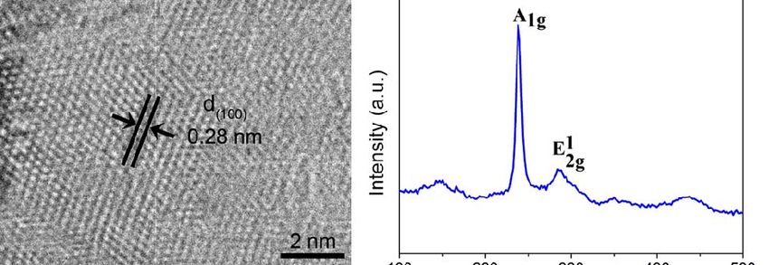
Figure S3. (a) SEM image, (b) XRD pattern, and (c) HRTEM image of the as-prepared hierarchical MoSe2
nanosheets, and (d) Raman spectrum showing the characteristic A1g (out-of-plane) and E12g (in-plane)
Raman modes located at 238.1 and 284.5 cm-1, respectively, for the MoSe2 nanosheets.
www.theNanoResearch.com∣www.Springer.com/journal/12274 | Nano ResearchNano Res.
Figure S4. (a) Schematic of the back-gated field effect transistor used for electrical measurements. (b)
Photograph of the FET. (c) Ids-Vds curves of the device at varied gate voltages (Vg) from – 40 V to 40 V. (d)
Ids-Vg curve at Vds = 2 V.
Figure S4 presents typical gate-dependent source–drain current (Ids) versus source–drain voltage (Vds)
curves measured at varied gate voltages (Vg) from −40 to 40 V in step sizes of 20 V, and the corresponding
Ids-Vg curve is shown. It is clear that the conductance of the MoSe2 nanosheets film increases (decreases)
consistently with the increase (decrease) of the gate voltage that was applied to the p + -Si back gate of the
nano-FET. It revealed the n-type nature of the MoSe2 nanosheets film, which are coincident with previous
reported results [1]. The field-effect electron mobility (μe) of the MoSe2 nanosheet film can be estimated to
be 2.8×10⁻⁴ cm 2 V −1 s −1 based on the following equation:
gm L
μe =
WCoxVds
Where L(18 μm) is the length of the channel, and W(10 μm) is width of the channel, respectively, Cox is
the capacitance per unit area (1.15×10⁻⁸ F cm-2), and gm is the trans-conductance of the device.
www.theNanoResearch.com∣www.Springer.com/journal/12274 | Nano ResearchNano Res.
Figure S5. (a) The I-V curves of the MoSe2 thin film/Si heterojunction measured under the dark and light
illumination, respectively, and (b) time response of the device under 650 nm light illumination at zero bias
voltage.
Figure S6. (a) The I-V curves of the Si/Graphene Schottky barrier diode measured under the dark and light
illumination, respectively, and (b) time response of the device under 650 nm light illumination at zero bias
voltage.
Figure S7. (a) The Schematic of graphene/MoSe2 nanosheets film used for determining the contact effect. (b)
The corresponding I-V curve of the device. Inset shows the photograph of the device.
In order to determine the contact effect of the MoSe2 nanosheets film/graphene, the graphene-MoSe2
nanosheets film-graphene was fabricated, as illustrated in Figure S7a. Figure S7b present the linear
current-voltage (I-V) curve, suggesting that such contact behavior could be proposed to be ohmic contact.
www.theNanoResearch.com∣www.Springer.com/journal/12274 | Nano ResearchNano Res.
Figure S8. (a) The Schematic of Ag/Graphene device used for determining the contact effect. (b) The
corresponding I-V curve of the device. Inset shows the photograph of the device.
Figure S8a shows the schematic of Ag-graphene-Ag device, and corresponding photograph shown in inset
of Figure S8b. It can be seen that the I-V curve exhibits linear behavior, indicating that the Ag electrode
shows excellent ohmic contact to graphene (Figure S8b).
Figure S9. Normalized frequency response of the Graphene/Si Schottky barrier diode.
www.theNanoResearch.com∣www.Springer.com/journal/12274 | Nano ResearchNano Res.
Figure S10. (a) Normalized photoresponse characteristic of the MoSe2 thin films/Si heterojunction at a
pulsed frequency of 50 kHz, and (b) normalized frequency response of the MoSe2 thin films/Si
heterojunction.
Figure S11. Capacitance measurement of the above mentioned three devices.
www.theNanoResearch.com∣www.Springer.com/journal/12274 | Nano ResearchNano Res.
Figure S12. The photoresponse characteristics of the solution-processed MoS2 nanosheets heterojunction. (a)
The I-V curves of the heterojunction measured under the dark and light illumination, respectively. Inset
shows the SEM image of the heterojunction and the TEM images of the MoS2 nanosheets, and (b)
normalized frequency response of the MoS2 nanosheets heterojunction.
Reference
[1] Chang, Y. H.; Zhang, W.; Zhu, Y.; Han, Y.; Pu, J.; Chang, J. K.; Hsu, W. T.; Huang, J. K.; Hsu, C. L.; Chiu,
M. H.; Takenobu, T.; Li, H.; Wu, C. I.; Chang, W. H.; Wee, A. T. S.; Li, L. J. Monolayer MoSe2 Grown by
Chemical Vapor Deposition for Fast Photodetection. ACS Nano 2014, 8, 8582-8590.
www.theNanoResearch.com∣www.Springer.com/journal/12274 | Nano ResearchYou can also read