EPITAXIAL MONOLAYER MOS2 ON MICA WITH NOVEL PHOTOLUMINESCENCE
←
→
Page content transcription
If your browser does not render page correctly, please read the page content below
Letter

                                                                                                                                pubs.acs.org/NanoLett

Epitaxial Monolayer MoS2 on Mica with Novel Photoluminescence
Qingqing Ji,† Yanfeng Zhang,*,†,‡ Teng Gao,† Yu Zhang,†,‡ Donglin Ma,† Mengxi Liu,† Yubin Chen,†
Xiaofen Qiao,§ Ping-Heng Tan,§ Min Kan,‡ Ji Feng,∥ Qiang Sun,‡,⊥ and Zhongfan Liu*,†
†
 Center for Nanochemistry (CNC), Beijing National Laboratory for Molecular Sciences, College of Chemistry and Molecular
 Engineering, Academy for Advanced Interdisciplinary Studies, Peking University, Beijing 100871, People’s Republic of China
‡
 Department of Materials Science and Engineering, College of Engineering, Peking University, Beijing 100871, People’s Republic of
 China
§
 State Key Laboratory of Superlattices and Microstructures, Institute of Semiconductors, Chinese Academy of Sciences, Beijing
 100083, People’s Republic of China
∥
  International Center for Quantum Materials, School of Physics, Peking University, Beijing 100871, People’s Republic of China
⊥
  Center for Applied Physics and Technology, Peking University, Beijing 100871, People’s Republic of China
    *
    S Supporting Information

    ABSTRACT: Molybdenum disulfide (MoS2) is back in the spotlight
    because of the indirect-to-direct bandgap tunability and valley related
    physics emerging in the monolayer regime. However, rigorous control of
    the monolayer thickness is still a huge challenge for commonly utilized
    physical exfoliation and chemical synthesis methods. Herein, we have
    successfully grown predominantly monolayer MoS2 on an inert and nearly
    lattice-matching mica substrate by using a low-pressure chemical vapor
    deposition method. The growth is proposed to be mediated by an epitaxial
    mechanism, and the epitaxial monolayer MoS2 is intrinsically strained on
    mica due to a small adlayer-substrate lattice mismatch (∼2.7%).
    Photoluminescence (PL) measurements indicate strong single-exciton
    emission in as-grown MoS2 and room-temperature PL helicity (circular
    polarization ∼0.35) on transferred samples, providing straightforward
    proof of the high quality of the prepared monolayer crystals. The
    homogeneously strained high-quality monolayer MoS2 prepared in this study could competitively be exploited for a variety of
    future applications.
    KEYWORDS: Molybdenum disulfide, chemical vapor deposition, van der Waals epitaxy, photoluminescence, valley polarization

M       onolayer molybdenum disulfide (MoS2), a two-dimen-
        sional (2D) hexagonal lattice composed of S−Mo−S
triple layers, has manifested a wealth of intriguing properties
                                                                          photocatalysts,13 solar energy funnels14 and excitonic integrated
                                                                          circuits.16
                                                                             However, these versatile applications demand large-scale
and spurred intense scientific interests. When bulk MoS2 is                development of monolayer MoS2 with the above-mentioned
thinned to the monolayer regime, an indirect-to-direct bandgap            properties. Conventionally, monolayer MoS2 is obtained via
transition occurs.1−4 This contributes to a strong photo-                 top-down exfoliation methods,1,2,6−10,15,17−20 which results in
luminescence (PL) with sensitive photoresponse.5−7 Moreover,              microscale flakes with a random distribution of film thickness.
the absence of centrosymmetry makes monolayer MoS2 valley-                Recently, several bottom-up methods, such as transition metal
selectively excited by circularly polarized light, reflected with          sulfurization,21,22 molybdenum oxide sulfurization,23−25 and
remarkable PL helicity.8−10 This facilitates a new conception of          decomposition of thiomolybdates,5,26,27 have been exploited to
valleytronics11 with the valley indexes serving as information            synthesize MoS2 on SiO2 and other insulating substrates.
carriers.                                                                 Nevertheless, the resulting films demonstrated a thickness
   Furthermore, monolayer MoS2 is an ultrastrength material12             ranging from monolayer to several layers. Hence, it is of critical
whose energy gap can be easily tuned via strain engineer-                 need to develop reliable strategies to synthesize macroscopically
ing.13,14 In addition, the greatly enhanced Coulomb interactions          uniform monolayer MoS2 that could be easily scaled up for
in the direct-gap monolayer MoS2 also make it a perfect model             batch production.
for exploring some fundamental issues of many-body correlated
quasiparticles, such as tightly bound trions15 in condensed               Received: May 27, 2013
matter physics. These unique functionalities make monolayer               Revised: June 24, 2013
MoS2 ideally suitable for applications, such as effective                  Published: July 30, 2013

                             © 2013 American Chemical Society      3870                         dx.doi.org/10.1021/nl401938t | Nano Lett. 2013, 13, 3870−3877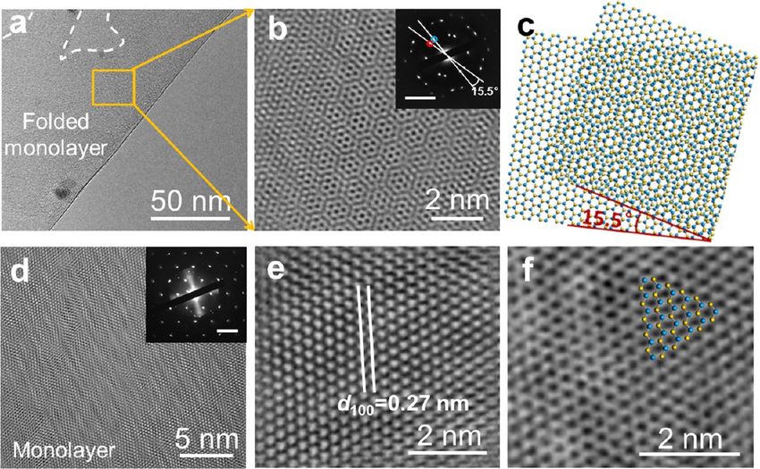
Nano Letters                                                                                                                                           Letter

Figure 1. LPCVD synthesis of MoS2 nano/microstructures on mica. (a) A schematic view illustrating the surface reaction during epitaxial growth of
MoS2. The upper panel gives probable occupation of MoS2 on mica. (b−d) SEM images showing the initial growth of MoS2 on mica. Inset in (c) is
the AFM profile of the MoS2 flake (scale bar 200 nm). (e) Statistical relation of surface nucleation density with flake size obtained from samples
shown in b−d (left to right correspondingly, statistics based on SEM images including at least 60 flakes); numbers above the graphs are the averaged
flake sizes.

   Fluorophlogopite mica (KMg3AlSi3O10F2) is considered to                     substrate: a(mica) = 0.531 nm, while a(MoS2) = 0.315 nm.
be a good van der Waals (vdW) epitaxy substrate for growing                    However, a(mica) approximates √3a(MoS2) (0.546 nm) with
2D materials, because of its atomic flatness, surface inertness,                a mismatch of −2.7% (negative sign means MoS2 lattice is
together with the hexagonally arranged in-plane lattice                        compressed), smaller than that of Cu(111) to graphene
characteristics. These features enable mica suitable for epitaxial             (∼3.9%). This indicates that the rotation of MoS2 lattice by
growth of materials possessing the same symmetry, such as                      30° would result in a commensurate structure with mica, which
topological insulators.28 In particular, the lattice symmetry of               may induce an epitaxial growth of MoS2 on it.
fluorophlogopite mica coincident with that of MoS2 could be                        The initial growth pattern of MoS2 on mica substrates, as
exploited for the epitaxial growth of monolayer MoS2 on mica.                  analyzed by using scanning electron microscope (SEM), is
   Herein, we have exploited vdW epitaxy to controllably                       shown in Figure 1b. The darker-contrast flakes on the surface
synthesize centimeter-scale uniform monolayer MoS2 on mica                     signify MoS2, and the surrounding regions correspond to the
through a low-pressure chemical vapor deposition (LPCVD)                       mica substrate. All the nucleated MoS2 flakes were triangular
process. Moreover, for the first time, we have unraveled the                    shaped, with same orientation and similar size, as highlighted
novel PL properties of this intrinsically strained monolayer                   using the dashed rhombus (Figure 1b). Upon prolonging the
MoS2, such as intense single excitonic emission on mica, and
                                                                               growth time, MoS2 enlarged in size (Figure 1c) to form larger
room-temperature PL helicity variation before and after
                                                                               triangular flakes. Detailed characterization of the sample using
transfer.
   Figure 1a schematically illustrates the surface reaction during             atomic force microscopy (AFM) demonstrates a flake thickness
the epitaxial MoS2 growth on mica substrates. Details on the                   of ∼0.7 nm, which is in conformity with that of monolayer
growth methodology and experimental setup are provided in                      MoS2 reported by previous studies.23,30,31 Further increase in
Supporting Information Section 1. In the typical process, MoO3                 the size of triangular MoS2 flakes to ∼3 μm (Figure 1d)
was partially reduced by sulfur vapor to form volatile MoO3‑x                  resulted in less straight edges, due to the formation of parallel
species,29 and subsequently they were conveyed downstream by                   kinks. These near triangular flakes are still considered to be
Ar carrier gas, adsorbed on mica, diffusing on the surface, and                 single crystals. Based on the experimental results reported in
reacting with sulfur to rearrange into MoS2 layers.                            previous studies, the edges of the triangles are empirically
                                                                               identified as sulfur terminated ones, along the zigzag
   S2 + MoO3 − x → MoS2 + SO2                                     (1)          orientation.32−34
   The upper half of Figure 1a shows the top view of atomic                       Statistical calculations of the flake size distribution and the
arrangement in mica and the probable occupation sites of                       nucleation density were subsequently determined (Figure 1e).
MoS2. It is noteworthy that there is a considerable lattice                    All the three histograms exhibited a Gaussian-distribution
mismatch in the in-plane periodicities of overlayer and                        shape, showing average island sizes of 0.32 ± 0.07, 0.78 ± 0.13,
                                                                        3871                         dx.doi.org/10.1021/nl401938t | Nano Lett. 2013, 13, 3870−3877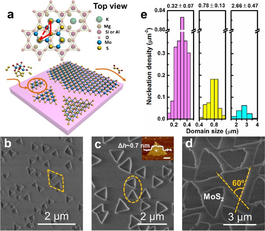
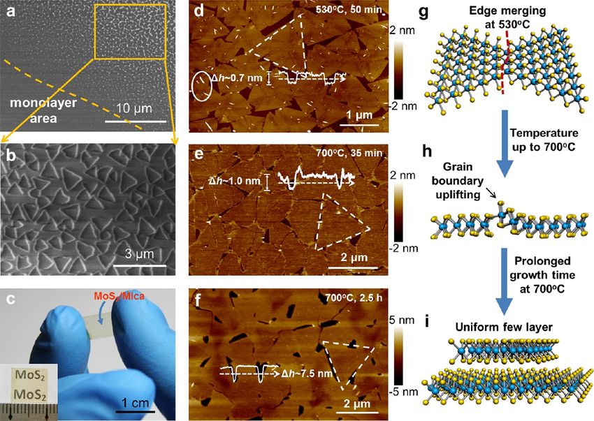
Nano Letters                                                                                                                                         Letter

Figure 2. Large-scale layered growth of MoS2 on mica. (a) Growth from submonolayer to monolayer (dashed orange line for eye guide) of MoS2 on
a partly sheltered mica substrate. (b) Magnified SEM image of the highlighted part in panel a. (c) Photograph of monolayer MoS2 with full coverage
on mica. (d) AFM profile of MoS2 sample with nearly full coverage (∼90%), grown at 530 °C for 50 min. The dashed triangle illustrates domain size
larger than 1 μm. (e,f) Uniform monolayer and multilayer MoS2 grown at 700 °C for 35 min and 2.5 h, respectively, with similar domain size of ∼2
μm. (g,h,i) Atomic models of different growth stages corresponding to panels d, e, and f, respectively.

and 2.66 ± 0.47 μm, corresponding to samples shown in Figure                 diameter
Nano Letters Letter
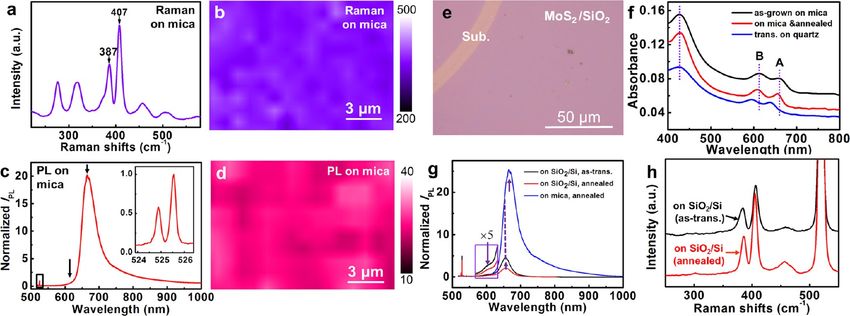
Figure 3. Spectroscopic characterization and transferability of monolayer MoS2 grown on mica. (a) Raman spectrum of as-grown monolayer MoS2
on mica. (b) Mapping of Raman characteristic peak intensity integrated from 370 to 420 cm−1 within a 15 × 10 μm2 area. (c) Normalized PL
spectrum of annealed monolayer MoS2/mica. The PL intensity is normalized by Raman A1′ phonon peak at ∼525.5 nm (407 cm−1 in Raman shifts).
The inset is the magnified spectrum showing characteristic Raman peaks. (d) Mapping of normalized PL intensity on the same area of panel c. (e)
Optical photograph of monolayer MoS2 transferred onto SiO2/Si. (f) UV−vis spectra of monolayer MoS2 before and after transfer. (g,h) Raman and
PL spectra, respectively, of the transferred MoS2. The PL intensity of B excitonic peak in panel g is 5-fold amplified to be identified clearly, and the
two lines in panel h are vertically offset.
growth time to 2.5 h resulted in uniform few-layered MoS2 with only in exfoliated monolayer MoS2 suspended on holed Si
a thickness of ∼7.5 nm (Figure 2f,i). substrates2 to our knowledge. Hence, the observation of single
We systematically characterized the monolayer MoS2 grown (A excitonic emission) peak is again a strong evidence that the
at 530 °C. Raman measurements performed on the sample monolayer MoS2 synthesized here is undoubtedly of high
(Figure 3a) exhibited two characteristic peaks, in parallel with quality. It is worth mentioning that the distinct peak tailing on
two phonon modes: out-of-plane vibration of S atoms (A′1) at the longer wavelength side is actually the PL background of
∼407 cm−1 and in-plane vibration of Mo and S atoms (E′) at mica substrates (see Supporting Information Figure S6).
∼387 cm−1, with a frequency difference Δ ∼20 cm−1. The PL spectrum was normalized by Raman A1′ peak
According to the “Δ-thickness relation” established by previous intensity, to rule out the external effects, such as laser power
works based on exfoliated samples,10,30,39 the observed and local electric field factors.1 The normalized PL intensity
frequency difference could be correlated to that of monolayer provided direct information on the PL quantum efficiency,
MoS2. which was observed to be significantly thickness dependent.1,2
Compared to the Raman spectra of exfoliated monolayer In the case of the monolayer MoS2/mica sample prepared in
MoS2 on SiO2/Si (A1′ and E′ peaks at ∼403 and 384 cm−1, this study, a strong PL intensity was usually accompanied by a
respectively30), a phonon mode stiffening, reflected with better Raman signal, as shown in Figure 3c. Hence the
blueshift of both characteristic peaks by 3−4 cm−1, was normalized PL intensity exceeding 20 could be regarded as PL
ubiquitously observed in all the samples prepared in this study. enhancement. In addition, the mapping of A peak intensity
This phenomenon is expected to be closely related to the (Figure 3d) was homogeneous over the whole region,
compressive strain induced by adlayer-substrate lattice demonstrating high thickness uniformity.
mismatch, as is similarly reported for strained graphene, Moreover, the prepared monolayer MoS2 sample (coverage
whose G and 2D peaks contemporarily red-shifted with >90%) was transferred intactly onto oxidized Si substrates
external tensile force.40,41 In any case, the phonon stiffening (with 300 nm oxide layer) with a portable transfer method. The
could be considered as an additional evidence of the epitaxial optical image of the transferred film (Figure 3e) shows a
growth. Additionally, we also performed the Raman mapping of uniform purple-like contrast corresponding to MoS2 across
MoS2 characteristic peak intensities (integrated from 370 to hundreds of micrometers, as distinguished from Si substrates
420 cm−1), to understand the thickness uniformity at the with a khaki color. Considering that MoS2 layers of different
micrometer scale (Figure 3b). It could be clearly evidenced that thickness may present distinct color contrasts in optical images,
the film is nearly homogeneous even at almost 10-μm scale, the nearly uniform contrast in the MoS2 regions indicate
except for bits of thicker areas dominating less than 5% of the uniform monolayer thickness. 32,42 To substantiate this
surface. conclusion, the intact nature of the transferred sample was
Figure 3c shows the typical PL spectrum of monolayer MoS2 also confirmed by using SEM (Supporting Information Figure
grown on mica obtained by annealing at 1000 °C under sulfur S7).
atmosphere. The reason for annealing the sample is explained Taking advantage of the transparency of mica in visible light
in Supporting Information Figure S5 and relevant discussions. region (Supporting Information Figure S4), we further
A strikingly strong PL peak (A excitonic emission) at ∼665 nm, conducted UV−vis absorption characterization of the as-
with no shoulder peak at ∼610 nm (B excitonic emission) was grown monolayer MoS2 sample (black line in Figure 3e).
observed (Figure 3c). Such single PL peak has been reported The resulting UV−vis spectrum exhibited two exciton
3873 dx.doi.org/10.1021/nl401938t | Nano Lett. 2013, 13, 3870−3877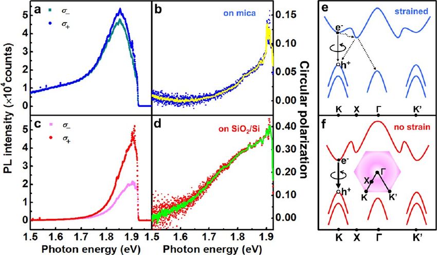
Nano Letters                                                                                                                                         Letter

Figure 4. HRTEM characterization of monolayer MoS2. (a) Folded edge of monolayer MoS2, with only one dark line contrast aligned at the edge.
(b) Zoomed-in image on (a) exhibits a randomly stacked region. Inset of (b) is the corresponding electron diffraction pattern (scale bar 5 nm−1).
Two sets of hexagonally arranged spots rotated by 15.5° were circled. (c) Atomic model of the folded edge. (d−f) Monolayer area with two typical
images shown in panels e and f. The inset of panel d is the diffraction pattern (scale bar 5 nm−1) for the monolayer area. (Panels d−f are filtered
HRTEM images. Original data can be found in Supporting Information Figure S8.)

absorption bands at 657 nm (1.89 eV) and 612 nm (2.03 eV),                   normalized intensity of A excitonic emission in the correspond-
labeled as A and B, respectively. These bands are believed to                ing PL spectra (Figure 3g) reduced significantly. These
originate from the direct bandgap transition at K point, with                observations imply that the charge impurity density of Si
energy split from valence band spin−orbital coupling.1,2 The                 substrates might have been improved further, as a result of
energy difference corresponding to the two peaks was observed                 annealing.
to be 0.14 eV, which is in good agreement with the theoretical                  High-resolution transmission electron microscopic
value of 0.148 eV, calculated for monolayer MoS2.43 This                     (HRTEM) analysis was performed to explore the monolayer
perfect agreement evidenced not only the fine electronic                      nature as well as the crystal quality of the prepared MoS2 after
structure, but also the high crystal quality of the prepared                 transfer. The low magnification HRTEM images (Supporting
monolayer MoS2/mica sample.                                                  Information Figures S10 and S11) exhibit a continuous film on
   Upon annealing the as-grown sample under sulfur atmos-                    the copper grids. Around the occasionally observed broken
phere at 1000 °C, the A and B absorption bands slightly                      regions, some obvious folding of the film could be clearly
blueshifted by 2 and 4 nm, respectively (red line in Figure 3f).             distinguished, based on the contrast with respect to the
However, when transferred onto quartz substrates (to                         adjacent regions (Figure 4a). In general, edge folding is a
corroborate PL spectra on SiO2/Si in Figure 3h), the resulting               common phenomenon in two-dimensional materials, like
sample exhibited two absorption bands (A and B) both                         graphene, which could be effectively utilized to determine the
blueshifted by ∼60 meV (blue line in Figure 3f). This suggests               number of layers.44 That is to say, the single dark line at the
probable band structure alteration during the transfer process.              folded edge could be correlated to a monolayer.
   We further recorded the PL spectra of MoS2 transferred onto                  The HRTEM image for the folded region exhibited a moiré
oxidized Si substrates. After transfer, the sample exhibited                 pattern with periodicity of ∼1.1 nm (Figure 4b), corresponding
typical PL features with A and B excitonic emission peaks                    to interlayer misorientation of ∼16°. This folding induced
centered at ∼656 and 605 nm, respectively (Figure 3g).                       misorientation was reconfirmed by the selected area electron
Notably, the PL intensity of monolayer MoS2 transferred on                   diffraction (SAED) pattern (inset of Figure 4b) collected over a
SiO2/Si was prominently weaker than that grown on mica. This                 scale of 200 × 200 nm2, which consists of two sets of
could probably be due to the enhanced charge trapping from                   hexagonally arranged diffraction spots rotated by ∼15.5° with
the SiO2/Si substrate. Meanwhile, A exciton PL peak                          each other. The first-order diffraction spots correspond to
blueshifted from ∼665 nm to ∼656 nm after transfer (Figure                   (100) planes, with which we calculated d(100) equaling 0.27
3g), consistent with the blueshifted absorption bands in the                 nm, thus MoS2 in-plane lattice constant a(MoS2) was
UV−vis spectra for transferred samples (blue line in Figure 3f).             determined to be ∼0.31 nm, which is in agreement with the
The concurrent blueshift observed in PL and absorption                       bulk value of 0.315 nm. For visualization, the atomic model of
spectra after transfer can be regarded as an evidence of the                 this folded edge is depicted in Figure 4c.
possible lattice strain releasing, considering the direct bandgap               We further examined the area away from the folded edge.
tunability of monolayer MoS2 via strain engineering.13,14                    The HRTEM images of this region reveal perfect atomic
   For comparison, we also annealed the MoS2 sample                          lattices extending over at least several hundred nanometers, as
transferred onto SiO2/Si substrate, at 900 °C under sulfur                   shown in Figure 4d. The corresponding SAED pattern shown
atmosphere. Figure 3h shows the Raman spectra of the                         as an inset exhibits only one set of diffraction spots, indicating
transferred sample before and after annealing. It could be                   the single crystalline nature of the film. Further high-resolution
observed that the annealing treatment enhanced the character-                images present two kinds of contrasts with triangular or
istic Raman peaks (Figure 3h). However, on the contrary, the                 hexagonal shape (Figure 4e,f), which agrees well with the data
                                                                      3874                         dx.doi.org/10.1021/nl401938t | Nano Lett. 2013, 13, 3870−3877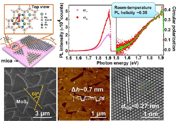
Nano Letters                                                                                                                                             Letter

Figure 5. Valley-polarized emission from our monolayer MoS2 before and after transfer. The helicity resolved PL spectra are shown in panels a and c,
and the corresponding circular polarization scatter-plotted as function of emissive photon energy are displayed in panels b and d. Panels a and b were
measured on monolayer MoS2/mica obtained by annealing at 1000 °C, while c and d were acquired on MoS2 transferred onto SiO2/Si. The
complementary colored curves inside b and d are adjacent-point-averaged results of circular polarization. (e) Schematic band structure along K-Γ-K′
direction for the compressively strained monolayer MoS2. Only the direct-gap emission at K valley (solid arrow) shows helicity, and the indirect-gap
transitions (marked with dashed arrows) give nonpolarized emissions. (f) Schematic band structure for monolayer MoS2 with zero strain. The first
Brillouin Zone of monolayer MoS2 is plotted as an inset.

published on exfoliated MoS2.45 The TEM results thus signify                        In summary, we have successfully synthesized centimeter-
that the MoS2 prepared in this study is almost defect-free and                   scale, strictly monolayer, high-quality MoS2 on the nearly
strictly monolayer.                                                              lattice-matching mica substrates, with the growth following an
   Furthermore, the high crystal quality of the prepared                         epitaxial mechanism. This synthesis method combines vdW
monolayer MoS2 was certified through its perfect valley related                   epitaxy with LPCVD, opening up the possibility of achieving
optical properties, considering that the PL helicity could be                    batch production of monolayer MoS2 with intrinsic strain in a
strongly reduced by intervalley scattering through defects and                   simple process. The high PL helicity (∼0.35) of transferred
impurities. For this, helicity resolved PL measurements were                     sample obtained at room temperature evidently demonstrates
performed on MoS2 before and after transfer (Figure 5). The                      the ultrahigh quality of the prepared MoS2, enabling it a
sample kept at room temperature (300 K) was excited with                         prototype for exploring valley related physics. That is, we
right-handed (σ+) circularly polarized He−Ne laser at 632.8                      believe the proposed strategy would pave the way for
nm. The degree of circular polarization can be defined as                         applications of CVD synthesized monolayer MoS2 in future
follows:                                                                         electronics and optoelectronics.
                                                                                    Methods. Monolayer MoS2 Epitaxial Growth and Trans-
              I(σ+) − I(σ −)                                                     fer. Large-area monolayer MoS2 were grown inside a multi-
   P(σ+) =
              I(σ+) + I(σ −)                                        (2)          temperature-zone tubular furnace (Lindberg/Blue M) equipped
                                                                                 with a 1-in.-diameter quartz tube. Sulfur powder was placed
where I(σ±) denotes the PL intensity of the right (left)-handed                  outside the hot zone, and was mildly sublimated with heating
component. Interestingly, as-grown monolayer MoS2 on mica                        belts at ∼100 °C. MoO3 powder (Alfa Aesar, purity 99.9%) and
exhibited a low PL helicity of less than 0.1 (Figure 5a,b);                      freshly cleaved fluorophlogopite mica substrates (thickness
whereas after the monolayer MoS2 was transferred onto SiO2/                      around 50 μm) were successively placed in the hot center
Si, P(σ+) dramatically increased to a maximum of ∼0.35                           inside the tube furnace. Argon was used as the carrier gas to
(Figure 5c,d). The observed high value of PL helicity at room                    convey MoO3−x vapor species to the downstream mica
temperature indicates a long lifetime for the photogenerated                     substrates. The tube was pumped down to a base pressure of
excitons in their original valley at K point (Figure 5f), strongly               ∼1 Pa and flushed with Ar carrier gas repeatedly to guarantee a
suggestive of the ultrahigh crystal quality of the CVD MoS2. By                  favorable growth atmosphere. Typical growth conditions were
contrast, the relatively low PL helicity for as-grown samples is                 pressure of 30 Pa, carrier gas flow rate of 50 sccm, growth
probably due to the band structure modulation of MoS2 by its                     temperature of 530 °C and growth time of 30−60 min.
conformation to the mica substrate. A direct-to-indirect                         Subsequently, the as-grown MoS2 sample was transferred to
bandgap transition (Supporting Information Figure S12)                           arbitrary substrates, such as oxidized silicon wafer, with the aid
probably occurs as demonstrated by our density functional                        of poly(methyl methacrylate) by using a portable transfer
theory (DFT) calculations where a small compressive strain of                    method. For this, hydrofluoric acid (20 wt %) was used as the
about −1.5% was applied. This would contribute more                              etchant to detach MoS2 adlayer from mica.
pathways for exciton relaxation to neighboring valleys (Figure                      Characterizations of Epitaxial Monolayer MoS2. The
5e indicated with dashed arrows), and hence the direct-gap                       prepared samples were systematically characterized using
recombination within the K valley was suppressed, correspond-                    optical microscopy (Olympus DX51), Raman spectroscopy
ing to a smaller PL helicity (for details, see Supporting                        (Horiba, LabRAM HR-800), UV−vis−IR (Perkin-Elmer
Information Section 7).                                                          Lambda 950 spectrophotometer), AFM (Vecco Nanoscope
                                                                          3875                         dx.doi.org/10.1021/nl401938t | Nano Lett. 2013, 13, 3870−3877
Nano Letters Letter
IIIa), SEM (Hitachi S-4800; acceleration voltage of 1−5 kV) (9) Mak, K. F.; He, K. L.; Shan, J.; Heinz, T. F. Nat. Nanotechnol.
and TEM (JEOL JEM-2100F LaB6; acceleration voltage, 200 2012, 7 (8), 494−498.
kV). A lacey carbon film supported on copper grids was used (10) Zeng, H. L.; Dai, J. F.; Yao, W.; Xiao, D.; Cui, X. D. Nat.
for TEM characterization, onto which MoS2 layer was Nanotechnol. 2012, 7 (8), 490−493.
transferred with the method described in the last paragraph. (11) Xiao, D.; Liu, G. B.; Feng, W. X.; Xu, X. D.; Yao, W. Phys. Rev.
Circularly Polarized PL Measurements. Helicity-resolved Lett. 2012, 108 (19), 196802.
(12) Bertolazzi, S.; Brivio, J.; Kis, A. ACS Nano 2011, 5 (12), 9703−
PL measurements were carried out using a Jobin-Yvon HR800
9709.
Raman system with an indigenously developed system for (13) Li, Y.; Li, Y.; Araujo, C. M.; Luo, W.; Ahuja, R. arXiv.org, e-Print
circularly polarized excitation. The excitation light of 633 nm in Arch., Condens. Matter 2012, No. arXiv:1211.4052, DOI: 10.1039/
wavelength, obtained using a HeNe laser, was passed through a C3CY00207A.
Soleil Babinet Compensator to generate a circularly polarized (14) Feng, J.; Qian, X.; Huang, C.-W.; Li, J. Nat. Photon. 2012, 6
light. The state of circular polarization was confirmed on the (12), 866−872.
sample location. An objective of relatively small numerical (15) Mak, K. F.; He, K.; Lee, C.; Lee, G. H.; Hone, J.; Heinz, T. F.;
aperture (0.55) was used to achieve close-to-normal-incidence Shan, J. Nat. Mater. 2012, 12 (3), 207−211.
excitation with negligible photon spin in the sample in-plane (16) High, A. A.; Novitskaya, E. E.; Butov, L. V.; Hanson, M.;
direction. The polarization was set to σ+, and the PL Gossard, A. C. Science 2008, 321 (5886), 229−231.
polarization (σ+ or σ−) was analyzed by using a quarter-wave (17) Eda, G.; Yamaguchi, H.; Voiry, D.; Fujita, T.; Chen, M. W.;
plate placed in front of a fixed Glan-Thomson linear polarizer. Chhowalla, M. Nano Lett. 2011, 11 (12), 5111−5116.
The whole setup provided a rejection ratio better than 5% in σ+ (18) Coleman, J. N.; Lotya, M.; O’Neill, A.; Bergin, S. D.; King, P. J.;
and σ− configuration, over the spectral range of interest. The Khan, U.; Young, K.; Gaucher, A.; De, S.; Smith, R. J.; Shvets, I. V.;
excitation power of 50 μW was used to avoid sample heating. Arora, S. K.; Stanton, G.; Kim, H. Y.; Lee, K.; Kim, G. T.; Duesberg, G.
■
S.; Hallam, T.; Boland, J. J.; Wang, J. J.; Donegan, J. F.; Grunlan, J. C.;
ASSOCIATED CONTENT Moriarty, G.; Shmeliov, A.; Nicholls, R. J.; Perkins, J. M.; Grieveson, E.
M.; Theuwissen, K.; McComb, D. W.; Nellist, P. D.; Nicolosi, V.
*
S Supporting Information
Science 2011, 331 (6017), 568−571.
Detailed description and discussion of the epitaxial CVD (19) Zeng, Z.; Yin, Z.; Huang, X.; Li, H.; He, Q.; Lu, G.; Boey, F.;
growth, temperature regulated growth mode, and explanation Zhang, H. Angew. Chem., Int. Ed. 2011, 50 (47), 11093−11097.
for the low PL helicity of as-grown monolayer MoS2 on mica, as (20) Li, H.; Yin, Z.; He, Q.; Li, H.; Huang, X.; Lu, G.; Fam, D. W. H.;
well as supplementary figures. This material is available free of Tok, A. I. Y.; Zhang, Q.; Zhang, H. Small 2012, 8 (1), 63−67.
charge via the Internet at http://pubs.acs.org.
■
(21) Kim, D.; Sun, D. Z.; Lu, W. H.; Cheng, Z. H.; Zhu, Y. M.; Le,
D.; Rahman, T. S.; Bartels, L. Langmuir 2011, 27 (18), 11650−11653.
AUTHOR INFORMATION (22) Zhan, Y. J.; Liu, Z.; Najmaei, S.; Ajayan, P. M.; Lou, J. Small
Corresponding Author 2012, 8 (7), 966−971.
*E-mail: yanfengzhang@pku.edu.cn (Y.Z.); zfliu@pku.edu.cn (23) Lee, Y. H.; Zhang, X. Q.; Zhang, W. J.; Chang, M. T.; Lin, C. T.;
(Z.L.). Chang, K. D.; Yu, Y. C.; Wang, J. T. W.; Chang, C. S.; Li, L. J.; Lin, T.
W. Adv. Mater. 2012, 24 (17), 2320−2325.
Notes (24) Wang, X.; Feng, H.; Wu, Y.; Jiao, L. J. Am. Chem. Soc. 2013, 135
The authors declare no competing financial interest.
■
(14), 5304−5307.
(25) Lin, Y. C.; Zhang, W. J.; Huang, J. K.; Liu, K. K.; Lee, Y. H.;
ACKNOWLEDGMENTS Liang, C. T.; Chu, C. W.; Li, L. J. Nanoscale 2012, 4 (20), 6637−6641.
This work was financially supported by the Ministry of Science (26) Liu, K. K.; Zhang, W. J.; Lee, Y. H.; Lin, Y. C.; Chang, M. T.; Su,
and Technology of China (Grant Nos. 2011CB921903, C.; Chang, C. S.; Li, H.; Shi, Y. M.; Zhang, H.; Lai, C. S.; Li, L. J. Nano
2012CB921404, 2012CB933404, 2013CB932603, Lett. 2012, 12 (3), 1538−1544.
2011CB933003, and 2009CB929301) and the National Natural (27) Shi, Y. M.; Zhou, W.; Lu, A. Y.; Fang, W. J.; Lee, Y. H.; Hsu, A.
Science Foundation of China (Grant Nos. 51222201, L.; Kim, S. M.; Kim, K. K.; Yang, H. Y.; Li, L. J.; Idrobo, J. C.; Kong, J.
51290272, 51121091, 51072004, 21073003, 11225421 and Nano Lett. 2012, 12 (6), 2784−2791.
10934007). (28) Li, H.; Cao, J.; Zheng, W.; Chen, Y.; Wu, D.; Dang, W.; Wang,
■
K.; Peng, H.; Liu, Z. J. Am. Chem. Soc. 2012, 134 (14), 6132−6135.
REFERENCES (29) Feldman, Y.; Wasserman, E.; Srolovitz, D. J.; Tenne, R. Science
1995, 267 (5195), 222−225.
(1) Splendiani, A.; Sun, L.; Zhang, Y. B.; Li, T. S.; Kim, J.; Chim, C. (30) Lee, C.; Yan, H.; Brus, L. E.; Heinz, T. F.; Hone, J.; Ryu, S. ACS
Y.; Galli, G.; Wang, F. Nano Lett. 2010, 10 (4), 1271−1275. Nano 2010, 4 (5), 2695−2700.
(2) Mak, K. F.; Lee, C.; Hone, J.; Shan, J.; Heinz, T. F. Phys. Rev. Lett. (31) Radisavljevic, B.; Radenovic, A.; Brivio, J.; Giacometti, V.; Kis, A.
2010, 105 (13), 136805.
Nat. Nanotechnol. 2011, 6 (3), 147−150.
(3) Huang, X.; Zeng, Z.; Zhang, H. Chem. Soc. Rev. 2013, 42 (5),
(32) van der Zande, A. M.; Huang, P. Y.; Chenet, D. A.; Berkelbach,
1934−1946.
T. C.; You, Y.; Lee, G.-H.; Heinz, T. F.; Reichman, D. R.; Muller, D.
(4) Chhowalla, M.; Shin, H. S.; Eda, G.; Li, L.-J.; Loh, K. P.; Zhang,
H. Nat. Chem. 2013, 5 (4), 263−275. A.; Hone, J. C. arXiv.org, e-Print Arch., Condens. Matter 2013,
(5) Tsai, D.-S.; Liu, K.-K.; Lien, D.-H.; Tsai, M.-L.; Kang, C.-F.; Lin, No. arXiv:1301.1985, DOI: 10.1038/nmat3633.
C.-A.; Li, L.-J.; He, J.-H. ACS Nano 2013, 7 (5), 3905−3911. (33) Lauritsen, J. V.; Kibsgaard, J.; Helveg, S.; Topsøe, H.; Clausen,
(6) Yin, Z. Y.; Li, H.; Li, H.; Jiang, L.; Shi, Y. M.; Sun, Y. H.; Lu, G.; B. S.; Lægsgaard, E.; Besenbacher, F. Nat. Nanotechnol. 2007, 2 (1),
Zhang, Q.; Chen, X. D.; Zhang, H. ACS Nano 2012, 6 (1), 74−80. 53−58.
(7) Choi, W.; Cho, M. Y.; Konar, A.; Lee, J. H.; Cha, G.-B.; Hong, S. (34) Helveg, S.; Lauritsen, J. V.; Lægsgaard, E.; Stensgaard, I.;
C.; Kim, S.; Kim, J.; Jena, D.; Joo, J.; Kim, S. Adv. Mater. 2012, 24 Nørskov, J. K.; Clausen, B.; Topsøe, H.; Besenbacher, F. Phys. Rev.
(43), 5832−5836. Lett. 2000, 84 (5), 951−954.
(8) Cao, T.; Wang, G.; Han, W.; Ye, H.; Zhu, C.; Shi, J.; Niu, Q.; (35) Chhowalla, M.; Amaratunga, G. A. J. Nature 2000, 407 (6801),
Tan, P.; Wang, E.; Liu, B.; Feng, J. Nat. Commun. 2012, 3, 887. 164−167.
3876 dx.doi.org/10.1021/nl401938t | Nano Lett. 2013, 13, 3870−3877Nano Letters Letter
(36) Remskar, M.; Mrzel, A.; Skraba, Z.; Jesih, A.; Ceh, M.; Demšar,
J.; Stadelmann, P.; Lévy, F.; Mihailovic, D. Science 2001, 292 (5516),
479−481.
(37) Bauer, E.; van der Merwe, J. H. Phys. Rev. B 1986, 33 (6), 3657−
3671.
(38) Peng, H.; Dang, W.; Cao, J.; Chen, Y.; Wu, D.; Zheng, W.; Li,
H.; Shen, Z.-X.; Liu, Z. Nat. Chem. 2012, 4 (4), 281−286.
(39) Zhang, X.; Han, W. P.; Wu, J. B.; Milana, S.; Lu, Y.; Li, Q. Q.;
Ferrari, A. C.; Tan, P. H. Phys. Rev. B 2013, 87 (11), 115413.
(40) Ni, Z. H.; Yu, T.; Lu, Y. H.; Wang, Y. Y.; Feng, Y. P.; Shen, Z. X.
ACS Nano 2008, 2 (11), 2301−2305.
(41) Huang, M. Y.; Yan, H. G.; Chen, C. Y.; Song, D. H.; Heinz, T.
F.; Hone, J. Proc. Natl. Acad. Sci. U.S.A. 2009, 106 (18), 7304−7308.
(42) Najmaei, S.; Liu, Z.; Zhou, W.; Zou, X.; Shi, G.; Lei, S.;
Yakobson, B. I.; Idrobo, J. C.; Ajayan, P. M.; Lou, J. arXiv.org, e-Print
Arch., Condens. Matter 2013, No. arXiv:1301.2812, DOI: 10.1038/
nmat3673.
(43) Zhu, Z. Y.; Cheng, Y. C.; Schwingenschlogl, U. Phys. Rev. B
2011, 84 (15), 153402.
(44) Meyer, J. C.; Geim, A. K.; Katsnelson, M. I.; Novoselov, K. S.;
Booth, T. J.; Roth, S. Nature 2007, 446 (7131), 60−63.
(45) Brivio, J.; Alexander, D. T. L.; Kis, A. Nano Lett. 2011, 11 (12),
5148−5153.
3877 dx.doi.org/10.1021/nl401938t | Nano Lett. 2013, 13, 3870−3877You can also read