FPGANIC: AN FPGA-BASED VERSATILE 100GB SMARTNIC FOR GPUS
←
→
Page content transcription
If your browser does not render page correctly, please read the page content below

FpgaNIC: An FPGA-based Versatile
                   100Gb SmartNIC for GPUs
    Zeke Wang, Hongjing Huang, Jie Zhang, Collaborative Innovation Center of
 Artificial Intelligence, Zhejiang University, China; Fei Wu, Collaborative Innovation
Center of Artificial Intelligence, Zhejiang University, China, and Shanghai Institute for
     Advanced Study of Zhejiang University, China; Gustavo Alonso, ETH Zurich
             https://www.usenix.org/conference/atc22/presentation/wang-zeke

     This paper is included in the Proceedings of the
       2022 USENIX Annual Technical Conference.
                        July 11–13, 2022 • Carlsbad, CA, USA
                                    978-1-939133-29-8

                                           Open access to the Proceedings of the
                                         2022 USENIX Annual Technical Conference
                                                     is sponsored by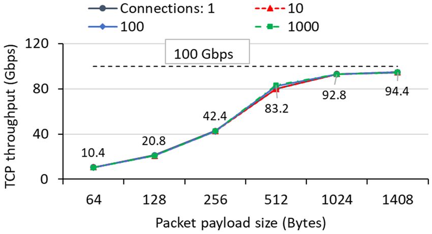
FpgaNIC: An FPGA-based Versatile 100Gb SmartNIC for GPUs

        Zeke Wang1 ,           Hongjing Huang1 ,           Jie Zhang1 ,       Fei Wu1,2                           Gustavo Alonso
    1   Collaborative Innovation Center of Artificial Intelligence, Zhejiang University, China        Systems Group, Dept. of Computer Science
              2   Shanghai Institute for Advanced Study of Zhejiang University, China                           ETH Zurich, Switzerland

                                 Abstract                                     NICs are common and soon 400Gbps will be available [46].
Network bandwidth is improving faster than the compute ca-                    This growing gap between network bandwidth and compute
pacity of the host CPU, turning the CPU into a bottleneck. As                 capability is being addressed through offloading of network
a result, SmartNICs are often used to offload packet process-                 functions to the Network Interface Card (NIC), so called
ing, even application logic, away from the CPU. However,                      SmartNIC [13, 14, 19, 36, 45], which frees up significant CPU
today many applications such as Artificial Intelligence (AI)                  cycles and provides better hardware to keep up with the grow-
and High Performance Computing (HPC) rely on clusters of                      ing network traffic and its often strict requirements in terms
GPUs for computation. In such clusters, the majority of the                   of bandwidth and latency.
network traffic is created by the GPUs. Unfortunately, com-                      Modern GPUs provide an order of magnitude higher mem-
mercially available multi-core SmartNICs, such as BlueFiled-                  ory bandwidth and higher compute capacity than modern
2, fail to process 100Gb network traffic at line-rate with its                CPUs. As a result, GPUs have become a key element in, e.g.,
embedded CPU, which is capable of doing control-plane man-                    Artificial Intelligence (AI) and High Performance Comput-
agement only. Commercially available FPGA-based Smart-                        ing (HPC) applications that are both compute- and memory-
NICs are mainly optimized for network applications running                    bound [4]. Since a multi-GPU server is often not enough to
on the host CPU. To address such scenarios, in this paper we                  cover the computing power needed in many AI, graph, and
present FpgaNIC, a GPU-oriented SmartNIC to accelerate                        HPC applications, current solutions are typically based on a
applications running on distributed GPUs. FpgaNIC is an                       cluster of GPUs (e.g., [27, 58, 78]), with the GPUS generating
FPGA-based, GPU-centric, versatile SmartNIC that enables                      the majority of the network traffic in such systems.
direct PCIe P2P communication with local GPUs using GPU                          In this paper, we present the design of a 100Gb GPU-centric
virtual address, and that provides reliable 100Gb network                     SmartNIC to serve distributed applications running on GPUs.
access to remote GPUs. FpgaNIC allows to offload various                      From a GPU’s perspective, such a SmartNIC should 1) enable
complex compute tasks to a customized data-path accelera-                     the GPU directly triggering doorbell registers and polling on
tor for line-rate in-network computing on the FPGA, thereby                   status registers on the SmartNIC without CPU intervention
complementing the processing at the GPU. The data-path                        (G1); 2) use the GPU virtual address space to directly access
accelerator can be programmed using C++-based HLS (High                       GPU memory via Peer-to-Peer (P2P) communication without
Level Synthesis), so as to make it easier to use for software                 CPU intervention (G2); 3) implement in hardware the full
programmers. FpgaNIC has been designed to explore the de-                     network stack to ensure low latency and high throughput
sign space of SmartNICs, e.g., direct, on-path, and off-path                  (G3); 4) support application logic offloading to a software-
models, benefiting different type of application. It opens up                 defined and hardware-accelerated data-path accelerator, i.e.,
a wealth of research opportunities, e.g., accelerating a broad                on-NIC computing processing 100Gb network traffic at line-
range of distributed applications by combining GPUs and                       rate (G4)1 ; and 5) The data-path accelerator should be easily
FPGAs and exploring a larger design space of SmartNICs by                     programmed by system programmers (G5). Commercially
making them easily accessible from local GPUs.                                available SmartNICs are not able to satisfy all these goals
                                                                              as they are not optimized for GPUs. In the following, we
1        Introduction                                                         analyze existing multicore and FPGA-augmented SmartNICs
While the computing capacity of CPUs is growing slowly                        that motivate FpgaNIC.
and mostly either through parallelism (SIMD, multi-core) or                   Multicore SmartNIC. A multicore SmartNIC, such as
specialization (GPGPU, security or virtualization support),                      1 In the paper, we use on-NIC computing module and data-path accelerator

network bandwidth is growing obviously faster. 100Gbps                        interchangeably.

USENIX Association                                                                       2022 USENIX Annual Technical Conference                    967
Table 1: Comparison of FpgaNIC with existing SmartNIC                  system. We have implemented FpgaNIC as a composable
types for GPUs. X indicates full support, %indicates no sup-           architecture that consists of a GPU communication stack,
port, and indicates partial support.                                   a 100Gb hardware network transport, and an On-NIC com-
                                        Multicore   FPGA-aug.
                                                                       puting (ONC), i.e., data-path accelerator.2 The GPU com-
                                        SmartNIC    SmartNIC    Ours   munication stack enables offloading of control plane onto
                                          [44]        [45]
                                                                       GPUs (G1) and thus for the first time enables local GPUs
      Control plane offload (G1)           %           %         X
 Access GPU with virtual address (G2)      X           %         X
                                                                       directly to manipulate SmartNIC without CPU intervention.
    100Gb transport offload (G3)                                 X     and enabling the FPGA-based SmartNIC for the first time to
  100Gb data-path accelerator (G4)         %                     X     use GPU virtual address to directly access GPU memory via
     High programmability (G5)             X           %         X
                                                                       PCIe P2P communication (G2). The 100Gb hardware net-
                                                                       work transport enables efficient and reliable 100Gb network
BlueField-2 [44], combines a multicore CPU, e.g., ARM, with            communication with remote GPUs (G3). Moreover, FpgaNIC
an ASIC network controller. It introduces an additional hop to         adopts a layered design to allow developers to easily explore
implement the smart function using a multicore CPU, which              the design space of SmartNIC models (i.e., direct, off-path,
features two DDR4 channels for staging. This allows to map             and on-path) to benefit their application, where different appli-
a broad range of applications on multicore SmartNICs. There-           cations favor a different SmartNIC model. FpgaNIC allows to
fore, its high programmability G5 is fully supported. However,         prototype applications that can eventually be migrated to hard-
it increases processing latency and multicore CPU’s mem-               ened SmartNICs. Implementing a data-path accelerator on
ory bandwidth can easily become a performance bottleneck.              an FPGA can easily satisfy line-rate processing requirement
BlueField-2 has 27.3GB/s achievable memory bandwidth un-               (G4) due to its hardware implementation, while FpgaNIC
der a benchmarking tool sysbench [1], indicating that directly         allows to use C++-based High Level Synthesis (HLS) so as to
staging 100Gbps data stream at the NIC CPU already over-               provide high programmability (G5). As such, in the context of
whelms BlueField-2, matching the findings in [40]. Therefore,          FPGA-GPU co-processing, the GPU provides to applications
it cannot act as a 100Gb data-path accelerator G4. To our              expressiveness and computing flexibility, while the FPGA
knowledge, the multicore SmartNIC is controlled from the               provides a flexible network infrastructure and the necessary
host CPU, so G1 is not yet supported. The network trans-               ONC. FpgaNIC results in significant end-to-end performance
port is implemented with the packet processing engine with             improvements as data can be processed as it flows from/to the
necessary control on the host (or ARM) CPU, so G3 is par-              GPU in a streaming manner and without involving the CPU.
tially supported. Finally, the ASIC network chip of multicore             We have prototyped FpgaNIC on a PCIe-based Xilinx
SmartNIC supports NVIDIA GPUDirect [52], which enables                 FPGA board Alveo U50 [74], whose UltraScale+ FPGA fea-
direct PCIe P2P data communication to a GPU, so G2 is fully            tures a 100Gbps networking port, a X16 PCIe Gen3, and
supported.                                                             8GB HBM. Its form factor is half-length, half-height and
FPGA-augmented SmartNIC. An FPGA-augmented                             its Maximum Total Power (MTP) is 75W, allowing it to be
SmartNIC combines a hardware-programmable FPGA                         easily deployed in any CPU server. 3 In addition to comprehen-
with an ASIC network controller. For example, Mellanox                 sive benchmarking, we validate the versatility and potential
Innova-2 [45] is an FPGA-augmented SmartNIC featuring                  of FpgaNIC by implementing use cases for all three mod-
a network adapter ConnectX-5 and an Xilinx FPGA.                       els: GPU-centric networking (in a direct model), a collective
ConnectX-5 consists of a 100Gbps InfiniBand/Ethernet                   primitive AllReduce (in an off-path model), and cardinality
interface for networking and a PCIe Gen4x8 interface for               estimation on incoming streaming data (in an on-path model).
communicating with the host CPU. The FPGA communicates                 The experimental results show that FpgaNIC is able to ef-
with ConnectX-5 via a PCIe x8 Gen4 link, so processing                 ficiently support all three SmartNIC models at the full line
packets on the FPGA adds considerable latency to the packets           rate of 100 Gbps Ethernet. Particularly, FpgaNIC-enhanced
and processing cannot happen at line rate because Innova-2             AllReduce almost reaches the maximum theoretical through-
has limited PCIe link bandwidth between the FPGA and                   put when performing on a distributed pool of eight RTX 8000
ConnectX-5. Therefore, Innova-2 can only acts as a partial             GPUs, while requiring fewer than 20% of the FPGA resources
100Gb data-path accelerator G4. G1 is not yet supported,               on the U50 board. It indicates that, even when considering
G2 is not supported, G3 is partially supported, and the high           the full network stack offloading, it has sufficient FPGA re-
programmability G5 is not supported.                                   sources to allow more aggressive offloading, e.g., the Adam
   Given the limitations of existing NICs, in this paper we
present FpgaNIC, a full-stack FPGA-based GPU-centric ver-                  2 In the paper, we use on-NIC computing module and data-path accelerator

satile SmartNIC that opens up the opportunity to explore a             interchangeably.
                                                                           3 We have also migrated FpgaNIC onto the Alveo U280 FPGA board [73]
large design space around SmartNICs due to the FPGA’s re-              with minor modifications affecting the FPGA pin mapping. Though we have
configuable nature and efficient FPGA-GPU co-processing                not ported FpgaNIC to Intel FPGA boards yet, we believe that it requires
while achieving all the five goals mentioned above in a single         only a small amount of effort to do so. We leave the porting to future work.

968   2022 USENIX Annual Technical Conference                                                                            USENIX Association
optimizer [31].4 As such, FpgaNIC enables efficient FPGA-                             Mem                Host CPU        (User code, GPU driver, FPGA driver)
GPU co-training on Deep Learning models. We leave this
exploration to future work.                                                                             PCIe Switch
                                                                                               Data plane:                          PCIe X16 Gen3
2     Design and Implementation of FpgaNIC                                                    FPGA—>GPU                        PCIe Endpoint

                                                                                                                                                                    GPU communication stack
                                                                                                                        Master               Slave
2.1     Design Challenges                                                                     Control plane:           Interface           Interface

We highlight four concrete research challenges we faced in                        GPUs        GPU—>FPGA                      DMA

                                                                                                                                                    Configuration

designing FpgaNIC.
C1: How to Enable the FPGA to Access the GPU Virtual                                                                        GTLB

Address? Enabled by NVIDIA GPUDirect [52], the DMA
engine in the PCIe IP core allows the FPGA to efficiently

                                                                                                                                                                    ONC
                                                                                                     HBM/DDR4          On-NIC Computing
transfer data from and to GPU memory via issuing a DMA

                                                                                                                                                                    HW Transport
read/write command that consists of a starting physical ad-
                                                                                                                      Network Transport
dress and length (no larger than a GPU page size). However,
doing so in the context of SmartNIC raises two challenges.                                                                         100Gb CMAC
First, a GPU program manipulates GPU virtual address rather                                                    100Gb Ethernet            FpgaNIC
than physical address, so the FPGA should work on GPU
virtual address to be consistent with the view of GPUs. Sec-
ond, a single contiguous virtual address space needs not to                  Figure 1: System architecture of FpgaNIC, which enables
be physically contiguous on GPU memory, and the typical                      control/data plane offloading and reliable network transport
memory page size is 64KB on modern GPUs as they do not                       offloading, and enables on-NIC computing module to process
yet support huge pages, making TLB management really chal-                   data from network at line rate. Moreover, FpgaNIC enables a
lenging, especially when the required number of TLB entires                  large SmartNIC design space exploration.
is large.
C2: How to Enable Efficient Reliable Network Transport                       scription language (HDL), which hinders FPGAs from wide
between Distributed GPUs? Modern GPUs have become a                          adoption by software programmers. Therefore, the program-
key compute engine to power AI and HPC applications due                      ming interface of FpgaNIC cannot be HDL so as to attract
to its massive parallel compute capacity and huge memory                     more system programmers.
bandwidth. AI and HPC applications typically need reliable                   C4: How to Enable Various SmartNIC Models? Based
network communication between distributed GPUs to realize                    on the location of the smart function, SmartNICs can be cat-
GPU-accelerated cluster computing. However, GPUs are not                     egorized into three models: direct, on-path and off-path. A
originally designed for reliable network transport [28, 43]                  direct SmartNIC allows local GPUs to directly manipulate the
since reliable networking reduces the degree of parallelism                  network transport to realize, e.g., GPU-centric networking.
and requires a complex flow control, e.g., retransmission.                      An on-path SmartNIC directly works on each network
   The straightforward approach to realize network transport                 packet according to the corresponding smart function so that
is to implement it on the CPU. Such a CPU-based approach                     packets do not need to be staged, avoiding unnecessary ad-
consumes several CPU cores to implement a 100Gbps net-                       ditional latency in calling the smart function. However, its
work transport layer. Furthermore, the network operations are                application scope is limited since it cannot handle complex
initiated from the GPU, incurring longer network latencies.                  functions as they are directly on the critical path of the net-
Instead, we offload the implementation of the reliable network               work packets.
transport to the FPGA to make the data plane fully bypass                       An off-path SmartNIC introduces an additional hop to
the host CPU. Fortunately, there is a growing amount of open-                implement the smart function using, e.g., a multicore CPU,
source FPGA-based 100Gb network transports [3] such as the                   which features two DDR4 channels for staging. This allows
TCP/IP stack of [57, 60] and the RoCEv2 stack used in [62].                  to map a broad range of applications on off-path SmartNICs.
However, how to enable the GPU to efficiently manipulate                     However, multicore CPU’s memory bandwidth can easily
the reliable hardware transport on the FPGA becomes a new                    become a performance bottleneck when processing 100Gb
challenge.                                                                   network traffic using the multicore CPU [40].
C3: How to Enable High-level Programming Interface                              Different smart functions favor different SmartNIC models.
for FpgaNIC? The traditional programming interface on                        For example, an on-path approach is preferred when offload-
FPGAs use tedious, low-level, cycle-sensitive hardware de-                   ing database’s filter operator [61] while AllReduce [4] is
   4 The total offloading tasks (communicator and optimizer) in FpgaNIC do   better mapped to off-path SmartNICs. Instead of using spe-
not need any GPU computing cycles that can be used for compute-intensive     cialized SmartNICs, we argue for a flexible architecture that
and memory-intensive forward and backward propagation.                       enables all this models.

USENIX Association                                                                     2022 USENIX Annual Technical Conference                                               969
2.2     Main Architecture of FpgaNIC                                GPU virtual address space so that the GPU program is able
To address the above four challenges, FpgaNIC adopts a lay-         to access these registers without CPU intervention. More-
ered design to enable easy design space exploration for Smart-      over, it enables us to populate GPU TLB (GTLB) entries on
NIC architectures dedicated for various distributed applica-        the FPGA such that the FPGA can translate GPU virtual ad-
tions that run on distributed GPUs, while minimizing the de-        dress to physical address before issuing a DMA read/write
velopment effort and increasing the overall system efficiency.      operation to GPU memory (§2.3.2).
FpgaNIC consists of three main components: GPU commu-
                                                                    2.3.2   Offloading Data Plane onto the FPGA
nication stack, reliable network transport in hardware, and
on-NIC computing (ONC), as shown in Figure 1. The goal of           FpgaNIC needs to offload the data plane onto the FPGA to
the GPU communication stack is 1) to allow the FPGA to use          allow the FPGA to directly access the GPU memory. How-
GPU virtual address (C1) to directly access GPU memory via          ever, NVIDIA GPUDirect [52] allows direct PCIe P2P data
direct PCIe P2P data communication at low-latency and line-         communication using physical address. For the sake of easy
rate, and 2) to allow GPUs to initiate data transfers by using      programming, FpgaNIC needs to work on GPU virtual ad-
doorbell registers on the FPGA to avoid having to involve           dress, rather than physical address (C1). Via a GPU BAR
the host CPU in the invocation. The goal of reliable network        window, Tesla GPUs expose all of their device memory space,
transport in hardware is to provide a reliable, low-latency, and    e.g., 40GB, while Quadro GPUs typically expose 256MB
high-throughput network access to the local GPUs (C2). The          memory space with 36MB reserved for internal use [52]. In
goal of on-NIC computing is 1) to enable high-level program-        order to allow the FPGA to access more GPU memory space,
ming interface, and 2) to enable three NIC models: direct,          FpgaNIC needs to store all the related virtual to physical
on-path, and off-path, such that FpgaNIC is able to benefit a       address translation entries. To minimize the overhead of trans-
broad range of GPU-powered distributed applications (C4).           lation, we intend to keep all the entries on on-chip memory.
                                                                    However, the 64KB GPU page size becomes the main chal-
2.3     GPU Communication Stack                                     lenge, because storing a great number of translation entries on
                                                                    the FPGA needs a large on-chip memory. For example, 32GB
Built on a PCIe IP core, e.g., Xilinx’s UltraScale+ Gen3 x16,       GPU memory needs 512K entries, far beyond the number
the GPU communication stack of FpgaNIC aims at enabling             the FPGA implementation can accommodate without hurting
offloading the control plane onto GPUs (via a slave interface)      timing.
and offloading the data plane onto the FPGA (via a master           How to Enable FPGA to Efficiently Work on Virtual Ad-
interface), such that the host CPU is bypassed.                     dress? To this end, we propose a GPU Translation Lookaside
                                                                    Buffer (GTLB) to perform address translation on the FPGA,
2.3.1    Offloading Control Plane onto GPUs
                                                                    while keeping the on-chip memory consumption reasonably
In order to allow GPUs to directly access the FPGA’s control        low. The key motivation behind the design of GTLB is that
and status registers, FpgaNIC needs to offload the control          even though a single contiguous virtual address space needs
plane onto the GPUs.                                                not be physically contiguous on GPU memory, it has high
How to Enable Control Plane Offloading? Enabling con-               probability to be physically contiguous, especially at the gran-
trol plane offloading requires a hardware-software codesign         ularity of 2MB. Therefore, we manually coalesce 32 consecu-
approach. On the hardware side, we enable a PCIe BAR ex-            tive 64KB GPU memory pages into a 2MB page if these 64KB
posing a configurable FPGA address space at the PCIe IP             pages are allocated to a contiguous portion of physical mem-
core on the FPGA. On the software side, our implementation          ory and aligned within the 2MB page. The GTLB consists of
consists of a GPU driver, an FPGA driver, and user code that        a main TLB and a complementary TLB. The process of popu-
interacts with both drivers. The process consists of three steps.   lating the GTLB on the FPGA involves four steps, as shown
First, the FPGA driver uses the function misc_register to reg-      in Algorithm 1. First, we pre-malloc GPU memory space us-
ister the PCIe BAR with the Linux kernel as an IO device            ing gpuMemAlloc for staging the GPU memory that will be
/dev/fpga_control. Second, the user code uses the function          accessed by the DMA engines on the FPGA (Line 1). Second,
mmap to map the device into the host address. Third, the user       we pass the initial virtual address and length of this GPU
code adopts a CUDA (Compute Unified Device Architecture)            memory to the GPU kernel function nvidia_p2p_put_pages
memory management function to register the host address             to get all the  pairs for all the 64KB pages (Line 2),
for use within a CUDA kernel [52]. With this, the GPU can           where VA refers to virtual address and PA refers to physical
directly trigger doorbell registers and poll status registers on    address. Third, we try to coalesce 64KB pages into 2M pages
the FPGA without CPU intervention.                                  as aggressive as possible (Line 3). Fourth, we populate main
What Control Plane Offloading can Do? After enabling                and complementary TLBs (Lines 4-18) via the control reg-
control plane offloading, the doorbell/status registers that are    isters exposed by the control plane offloading (§2.3.1). The
instantiated by all the components (GPU communications              main TLB provides the virtual to physical address translations
stack, ONC, and network transport) have to be mapped into           for 2MB pages (Lines 7-10). If any 2MB page is not physi-

970     2022 USENIX Annual Technical Conference                                                              USENIX Association
Algorithm 1: P OPULATING GTLB 2.4 100Gbps Hardware Network Transport
Input : init_addr: initial GPU virtual address In order to address the second challenge (C2), FpgaNIC of-
len: length of GPU memory
Output : T LBmain : main TLB floads the transport-layer network to the FPGA to provide a
T LBcomp : complementary TLB reliable and high-performance hardware network transport
/* Step 1: Malloc GPU memory space. */
1 init_addr = gpuMemAlloc(len); to the local GPUs. Fortunately, there is a growing amount of
/* Step 2: Get pairs of all the 64KB pages. */ open-source FPGA-based 100Gb network stacks such as the
2 pairs = nvidia_p2p_put_pages (init_addr, len);
/* Step 3: Coalescing 64KB pages to 2MB pages if possible */ TCP/IP stack of [57, 60] and the RoCEv2 stack used in [62].
3 pairsTable 2: Resource Usage breakdown of FpgaNIC on U50. Table 3: Two interfaces of GPU communication stack
LUTs REGs RAMs DSPs Type Interface Content
Slave interface axilite_control AXI-Lite interface for configuration
Available 871K 1743K 232.4Mb 9024
Master interface dma_read_cmd Dest. GPU virtual address, length
GPU Commu. Stack 79K 103K 5.2Mb 0 dma_read_data AXI data stream from GPU memory
100G HW Transport 101.3K 166.5K 23.4Mb 0 dma_write_cmd Source GPU virtual address, length
ONC: GPU-centric networking 14.5K 20K 24.6Mb 0 dma_write_data AXI data stream to GPU memory
ONC: AllReduce 7.3K 10K 12.8Mb 0
ONC: Hyperloglog 19.5K 26K 7.1Mb 1104
Table 4: Manipulation interface for the network transport
and data transfer and assembles the complete data stream for Type Interface Meaning
Data interface tcp_tx_meta Session ID, length
each TCP connection without programmer’s involvement in tcp_tx_data AXI data stream to remote node
depacketization. tcp_rx_meta Session ID, length, IP, port, etc.
tcp_rx_data AXI data stream from remote node
Control interface server_listen_port A TCP listening port
2.5 On-NIC Computing (ONC) server_listen_start Staring to listen
client_conn_port Destination port to connect
The on-NIC computing module sits between the GPU com- client_conn_ip Destination ip to connect
munication stack module and the 100Gbps network hard- client_conn_start Start to connect to server
conn_close_session Destination session to connect
ware transport module, so ONC can directly manipulate the conn_close_start Start to close connection
other two modules to enable flexible design space exploration
around GPU-centric SmartNICs. The key goal of on-NIC
computing module is to 1) expose high-level programming in- up to 4G. The data from and to GPU memory is sent over the
terface for system programmer, and 2) enable three SmartNIC dma_read_data and dma_write_data data streams, which
models for various GPU-powered distributed applications. In are 64B-wide AXI-Stream interfaces. For either GPU mem-
the following, we discuss the programming interface of ONC ory read or write operation, we need to configure the com-
and how to enable three three models. mand stream and then work on the corresponding data stream,
2.5.1 High-level Manipulation Interfaces of ONC allowing programmers to easily access GPU memory.
In order to address the third challenge (C3), FpgaNIC intends Interfaces of Hardware Network Transport. The hardware
to raises the programming abstraction from HDL to high-level network transport exposes two interfaces: data interface and
synthesis (HLS), i.e., C/C++, such that systems programmers control interface.
are able to use C/C++ to manipulate FpgaNIC, rather than The data interface consists of a sending interface and a re-
cycle-sensitive HDL.7 In the following, we present the con- ceiving interface. The sending interface consists of a metadata
crete manipulation interfaces for the GPU communication stream and a data stream. The metadata stream (tcp_tx_meta)
stack and hardware network transport modules. is a 48-bit-wide AXI-Stream that provides a 4B-wide data
Manipulation Interfaces of GPU Communication Stack. length and a 2B-wide session ID that corresponds to a re-
The GPU communication stack exposes two manipulation in- mote node. The data stream (tcp_tx_data) is a 64B-wide
terfaces: a slave interface that allows GPUs to access FPGA’s AXI-Stream to send payload stream. The receiving interface
registers and a master interface that allows the FPGA to di- also consists of a metadata stream and a data stream. The
rectly access GPU memory, as shown in Table 3. metadata stream (tcp_rx_meta) is an 44B-wide AXI-Stream
The slave interface is a 4B-wide AXI-Lite interface that provides session ID, length, IP address, port and close
(axilite_control), through which local GPUs directly access session flag. The data stream (tcp_rx_data) is a 64B-wide
doorbell and status registers within FpgaNIC without CPU AXI-Stream to receive payload stream from remote node.
intervention. In FpgaNIC, we instantiate 512 doorbell regis-
The control interface of the hardware transport is similar
ters and 512 status registers, each of which has its own PCIe
to that of the well-understood socket interface, which allows
address to allow individual access. We correspond a few door-
GPU programmers to easily leverage the network transport,
bell and status registers to each engine from any of three
with their meanings as shown in Table 4. We instantiate the
components within FpgaNIC. The doorbell registers can be
corresponding doorbell and status registers, exposed through
triggered by GPUs to manipulate the engine, and the status
the PCIe’s slave interface (§2.3), to allow local GPUs to di-
registers can be polled by GPUs to check the status of the
rectly manipulate or poll the 100Gb hardware network trans-
engine.
port.8 In summary, the network transport serves as a network
The master interface consists of two command streams
proxy, through which the ONC module and local GPUs can ac-
and two data streams. The two command streams are
cess the network transport directly without CPU intervention,
96-bit-wide AXI-Stream interfaces (dma_read_cmd and
so as to address the second challenge C2.
dma_write_cmd) that provide the GPU virtual address and
length to directly access GPU memory, where the length is
8 Inside
the FPGA, the ONC module (§2.5) can also directly manipulate
7 Nevertheless, ONC can be also programmed in HDL if necessary. the hardware transport via these registers.
972 2022 USENIX Annual Technical Conference USENIX AssociationTable 5: Lines of code for each component of FpgaNIC
…
Server 0 Server 1 Server 7
Hardware Software CPU CPU CPU
GPU Commu. Stack 2.9K (Verilog/HLS) 0.7K (C++, CUDA) GPUs GPUs GPUs
100G HW Transport 15.3K (HLS)
ONC: GPU-centric networking
ONC: AllReduce
1.0K (HLS)
2.7K (HLS/Verilog)
0.5K (C++, CUDA)
1.5K (C++)
FpgaNIC FpgaNIC … FpgaNIC
ONC: Hyperloglog 1.6K (HLS) 0.3K (C++, CUDA)
100GbE 100GbE 100GbE
100Gb Ethernet Switch
2.5.2 How to Support Three SmartNIC Models?
In order to address the fourth challenge C4, FpgaNIC’s on- Figure 2: Experimental Setup
NIC computing component allows system programmers to implementation of AllReduce with FpgaNIC is in the Ap-
customize data-path engines between the GPU communica- pendix §A.2.9
tion stack and the hardware network transport to accelerate
How to Support Multiple Tenants? To support multiple
various distributed applications. Table 2 shows that the pre-
tenants, we can adopt Coyote [32] to wire the GPU communi-
vious GPU communication stack and network transport con-
cation stack and hardware network stack into the static region
sume less than 20% FPGA resources on a mid-sized FPGA
of FpgaNIC while exposing the same programming interface
U50, so the on-NIC computing component has plenty of re-
to offloaded tasks, for which we pre-synthesize the FPGA
sources to realize complex data-path engines to accelerate
bitstreams ahead of time. Furthermore, FpgaNIC adopts the
various distributed applications. Moreover, the commercial
notion of vFPGAs (virtual FPGAs or separate application
FPGA board that features DDR4 (even HBM) is able to stage
regions that are individually reconfigurable) as implemented
data from network or GPUs, and perform on-NIC comput-
in Coyote [32] to smoothly support secure, temporal and spa-
ing on the data before feeding into GPUs or sending out to
tial multiplexing of GPU communication stack and hardware
network.
network transport between tenants (without pre-emption and
Due to the reconfigurable nature of the FPGA, FpgaNIC context switching). For each tenant, FpgaNIC provides suffi-
can easily support various SmartNIC models: direct, on-path, cient FPGA resources in a partial reconfiguration region to
and off-path, to benefit a broad range of distributed applica- implement an independent ONC engine to guarantee perfor-
tions. Table 5 shows the lines of code for each component. mance isolation, and thus we no longer need to reboot the
The direct model directly exposes the hardware network FPGA to change the functionality of FpgaNIC. We leave this
transport module to local GPUs via the GPU communication as future work.
stack module, such that local GPUs can directly manipulate
the network transport to do reliable network communication. 3 Experimental Evaluation
An an example, we develop a GPU-centric networking to
demonstrate the potentials of the direct model. Due to space 3.1 Experimental Setup
limitation, we describe the detailed design and implementa-
System Architecture. The experiments are run on a clus-
tion of GPU-centric networking to the Appendix §A.1.
ter consisting of eight 4U AMAX servers, connected with a
The on-path model is similar to the direct model that local
Mellanox 100Gbps Ethernet SN2700 switch (Figure 2). Each
GPUs directly manipulate the hardware network transport,
server is equipped with two Intel Xeon Silver 4214 CPUs
except that the on-path model allows the network stream also
@2.20GHz, 128GB memory, FpgaNIC (i.e., a Xilinx Ultra-
to enter an on-path engine in the ONC component for the
Scale+ FPGA [72]), and a Nvidia RTX 8000 GPU, where the
offloaded computation, where the on-path engine needs to
FPGA and the GPU have direct PCIe P2P communication, as
consume the network stream at line-rate such that the on-path
shown in Figure 1. Two servers have an additional two A100
engine would not impede line-rate network traffic. We use
GPUs. FpgaNIC is implemented on Xilinx Alveo cards U50
the HyperLogLog (HLL) application [18, 33] as an example
or U280 with Vivado 2020.1.
to demonstrate the power of the on-path model. The detailed
Methodology. We first benchmark the GPU communication
design and implementation of HLL with FpgaNIC can be
stack and hardware network transport to demonstrate that Fp-
found in the Appendix §A.3.
gaNIC allows easy PCIe P2P communication with local GPUs
The off-path model enables an off-path engine in the ONC and reliable network communication with remote GPUs. We
component to directly manipulate the GPU communication then evaluate the three FpgaNIC models: direct (§3.3), off-
stack and the hardware network transport such that FpgaNIC path (§3.4), and on-path (§3.5), to demonstrate FpgaNIC’s
is able to orchestrate the data flow between all the three com- performance and ability to enable the exploration of a large
ponents. Typically, the off-path needs to stage data in on- SmartNIC design space.
board memory. We use the collective communication primi- 9 The off-path model is generic enough such that it would also work well
tive AllReduce [4, 11, 50] as an example to demonstrate the in other applications that follow a partition/aggregate pattern and require
power of the off-path model (§A.2). The detailed design and multiple rounds of communication [38].
USENIX Association 2022 USENIX Annual Technical Conference 9733.2 Benchmarking Shared Infrastructure
We benchmark the shared GPU communication stack and
hardware network transport.
3.2.1 GPU Communication Stack
To analyze the effect of control plane and data plane offload-
ing, we measure the latency and throughput of the PCIe P2P
link (§2.3). We use two classes of GPU: Quadro RTX8000
(labelled “R8K") and Tesla A100 (labelled “A100"), since a
different GPU class leads to different latency and throughput.
Effect of Control Plane Offloading. We examine the effect
of control plane offloading by comparing the latency of com- Figure 4: PCIe P2P throughput between FPGA and GPU
mands issued from the GPU to the FPGA. Figure 3 shows the
read latency when using various end points: “X_Y" means 3.2.2 Hardware Network Transport
that device “X" reads from device “Y". A first important re- Next, we measure the throughput and latency of the hardware
sult is that the latency of interactions between the GPU and network transport (§2.4).
the FPGA is comparable to that of the CPU calling the FPGA Latency. We measure the the round-trip time (RTT) between
and it is under 1 microsecond. Moreover, the GPU-FPGA’s two FPGAs connected via the network switch. Figure 5a
latency fluctuation is smaller than that of CPU-FPGA, demon- shows the RTT with varying message size. The most striking
strating one of the advantages of FpgaNIC in terms of offering result is that the TCP latency is in microseconds, instead of
deterministic latency. The results also show that performance milliseconds, demonstrating the advantages of offloading to
improves slightly with a better GPU, indicating that the overall a SmartNIC instead of using the CPU for communication.
system will improve with future versions of the GPU. Finally, For messages smaller than 1 KB, the RTT latency (roughly
the latency of “GPU_FPGA" is significantly lower than that 3.1us) is dominated by the physical communication path (the
of “GPU_CPU" plus “CPU_FPGA", proving the efficiency Ethernet switch introduces an additional hop with roughly
of control plane offloading proposed in FpgaNIC. 1us latency.
Throughput. We measure as well the throughput between
2 two network transports with varying packet size and vary-
ing number of connections. Figure 5b shows the observed
Latency [µs]
1.5
throughput by sending out a total of 1GB from one transport to
1 the other with varying packet size and number of connections.
We observe that the number of connections does not affect the
0.5 achievable throughput under the same packet size, indicating
that FpgaNIC is able to efficiently support multi-connection
0 communication. For small packets, the throughput is low due
R8K_FPGA A100_FPGA CPU_FPGA R8K_CPU A100_CPU
to the fixed overhead, i.e., the 40B header, per packet and the
Figure 3: Control plane latency comparison. X_Y refers to
turnaround cycles to process each packet. However, for larger
the device “X" accesses the device “Y". R8K refers to RTX
packets, the achievable throughput is close to the 100Gbps
8000 GPU, and A100 refers to A100 GPU. Whiskers show
channel capacity, demonstrating that FpgaNIC efficiently uses
the 1st and 99th percentile.
the available network bandwidth.
Effect of Data Plane Offloading. We examine the effect of
data plane offloading by measuring the throughput when the 3.3 Evaluation of the Direct Model
FPGA issues a DMA read/write operation to GPUs. Each We evaluate the throughput of FpgaNIC used in direct mode.
operation transfers 4GB of data between the FPGA and the The experiment involves sending data from one GPU to a
GPU memory. Figure 4 illustrates the achievable throughput remote GPU through the corresponding FPGAs using the
with varying burst size, which is associated with the length of direct model path: GPU-PCIe-FPGA-network-FPGA-PCIe-
a DMA operation. It is interesting to observe that DMA read GPU.
and write operations reach peak throughput at different burst
Effect of Slot Size. We examine the effect of the slot size
sizes: 512B for read and 8K for write, indicating that we need
(W ) of the circular buffer for each connection (§A.1.2). The
to carefully choose the right DMA size to saturate the PCIe
slot size determines the size of the DMA operation between
P2P bandwidth between FPGA and GPU. As with latency,
an FPGA and a GPU. Figure 6a illustrates the throughput
a newer GPU class leads to much higher PCIe throughput.
with varying slot size. We have two observations. First, a
For example, a DMA read operation to an A100 GPU yields
sufficiently large slot size leads to saturated throughput. A
12.6GB/s, close to the maximum possible PCIe bandwidth.
974 2022 USENIX Annual Technical Conference USENIX Association(a) Effect of DMA size with control plane offloading
(a) Round-trip latency with varying message size
(b) Throughput with varying packet size and connections (b) Effect of control plane offloading on chunk size
Figure 5: 100Gb TCP stack: latency and throughput
small slot size (AllReduce engine) but also part of the learning engine such
as the compressor (e.g., compression engine) and optimizer
(e.g., Adam engine) to FpgaNIC, such that the entire commu-
nication part of training is offloaded to minimize the commu-
nication overhead for GPUs. Since these engines can easily
achieve line-rate throughput, plenty of interesting trade-offs
in the design of distributed learning, e.g., sync vs. async, can
be revisited by using FpgaNIC. We leave this idea to future
Figure 7: Effect of data size under eight nodes work.
3.5 Evaluation of the On-path Model
We finally evaluate the performance of FpgaNIC-enhanced
HLL, when FpgaNIC is configured in an on-path model. The
cardinality is calculated when the data stream has been trans-
ferred. The goal of this experiment is to verify whether the
HLL module within an FPGA can act as a bump in the wire.
The baseline, labelled “write", is to feed data to a GPU
without processing the data in the FPGA. The GPU receives
Figure 8: Effect of node number with 64MB data size the data from the FPGA and stores it in the current block in
GPU memory, while at the same time performing HLL on
Comparison Metric. To demonstrate the performance of the previous block, overlapping data transfer with cardinality
AllReduce, we introduce the metric bus bandwidth [51], calculation at the block granularity. Table 6 illustrates that at
which is calculated to be algorithm bandwidth times 2 ∗ (N − least 8 SMs, in terms of 8 thread blocks and 512 threads per a
1)/N, where algorithm bandwidth is calculated to be the data thread block, are required to consume 100Gbps data stream
size divided by the elapsed time and N is the number of nodes. (packet payload size: 1408 bytes) on an A100 GPU, when
The elapsed time is estimated to be the average time of all the the block size is no smaller than 256K. Moreover, when the
involved nodes in five rounds [9]. block size is smaller than 128K, an A100 GPU is not able to
Effect of Data Size. We examine the effect of data size when consume the data stream, as such a small block size cannot
performing AllReduce. Intuitively, a large data size easily fully utilize GPU’s processing parallelism.
leads to a saturated throughput because we hit the bandwidth
limits of the underlying channels. Figure 7 illustrates the bus Table 6: Number of required GPU SMs w.r.t block size
bandwidth comparison between FpgaNIC and NCCL in a clus- Block size 256 8 8 8
NCCL, because the AllReduce engine in FpgaNIC efficiently
overlaps the operations of the PCIe DMA, network transport,
and FPGA memory. Moreover, FpgaNIC does not consume
any GPU/CPU cycles, freeing up these precious computing
resources for other important tasks. FpgaNIC reaches the the-
oretical bus bandwidth when the data size is larger than 8MB,
indicating that FpgaNIC’s AllReduce implementation is us-
ing all resources efficiently. Finally, when data size is small
(Table 7: Comparison of FpgaNIC with existing SmartNICs from industry. X indicates full support, %indicates no support.
Programmable flow processing Targeted applications CPU-centric GPU-centric
Broadcom [7] X Virtualization, storage, NFV X %
Pensando [53] X Storage, security X %
Netronome [49] X SDN-controlled server-based networking X %
Intel IPU [23, 24] X Cloud, storage, security X %
FpgaNIC X AI model training % X
e.g., at least 8 A100 SMs, which can be used in other comput- done [12, 16, 29, 41, 42, 44, 47, 48, 54, 56, 63, 66, 70] on Smart-
ing task. Moreover, Table 2 shows that FpgaNIC-enhanced NIC built upon a wimpy RISC cores plus hardware engines
HLL takes a small amount of FPGA resources. Therefore, in to accelerate dedicated functionality such as compression.
the context of FPGA+GPU co-processing, it is clearly more These RISC cores are used to both process packets as well
efficient to offload HLL onto FpgaNIC, rather than processing as to implement “smart" functions instead of using the host
HLL on the GPU. CPUs. Such an approach inevitably suffers from load inter-
ference since packet processing and the smart functions have
4 Related Work to compete for the shared resources, e.g., the last level cache
To our knowledge, FpgaNIC is the first FPGA-based GPU- and memory bandwidth. In contrast, FpgaNIC implements an
centric 100Gbps SmartNIC that addresses the bottleneck lim- GPU-centric SmartNIC on an FPGA.
itations introduced by the use of conventional CPUs or small
cores (ARM) in SmartNICs. On-going SmartNICs in Industry. Besides NVIDIA’s
FPGA-augumented SmartNICs. Several commercial sys- DPU, we compare FpgaNIC with other SmartNICs from in-
tems [10, 21, 22, 45, 55, 79] feature an FPGA within a Smart- dustry, as shown in Table 7. Broadcom offers the Stingray
NIC. The closest work is from Mellanox Innova [45] that SmartNIC [7], which features a ARM 8-core CPU for control-
features an FPGA in its SmartNIC to accelerate offloaded plane management and P4-like TruFlow packet processing
compute-intensive applications, while PCIe and network in- engine for data-plane processing, targeting various applica-
terfaces are handled by a NIC ASIC ConnectX-5. The FPGA tions such as virtualization, storage, and NFV. Pensando has
is connected with the NIC ASIC via a PCIe interface and a DPU architecture [53] that features an ARM CPU and a
therefore acts as an additional PCIe endpoint. The FPGA P4 processor for data-plane packet processing, targeting var-
is entirely dedicated to the user’s application logic. In con- ious applications such as security and storage. Netronome
trast, FpgaNIC implements all functionalities, including net- provides the NFP4000 Flow Processor architecture [49] that
working and PCIe, within a powerful FPGA, enabling a large features a ARM CPU, 48 packet processing cores, and 60
design space exploration of SmartNIC architecture, while In- P4-programmable flow processing cores for data-plane pro-
nova provides limited architectural flexibility due to how the cessing, targeting the SDN-controlled server-based network-
FPGA is connected. ing application. Intel presents the FPGA-based IPU (Infras-
GPU-FPGA Communication. Previous work [6, 64] has im- tructure Processing Unit) that consists of a MAX 10 FPGA
plemented GPUDirect RDMA on an FPGA to directly ac- for control-plane management and an Arria 10 FPGA for
cess GPU memory, but not allowing the GPU to trigger door- data-plane processing [23], and uses an ASIC IPU whose
bell registers within an FPGA. In contrast, FpgaNIC allows architecture is not publicly documented [24]. Fungible has
GPUDirect RDMA and the GPU to trigger registers within a DPU [15] featuring multiple PCIe endpoints, TrueFabric
an FPGA, and is an FPGA-based SmartNIC that allows large for networking, and specialized engines such as compression
design space exploration of SmartNIC architecture. and EC/RAID to address inefficient data-centric computa-
Acceleration using FPGA-based SmartNICs. Most previ- tion within a node and inefficient interchange between nodes,
ous work [2, 3, 8, 10, 13, 14, 14, 17, 26, 35, 36, 36, 37, 59, 62, 65] targeting various applications such as virtualization, cloud
features an FPGA on SmartNICs to offload data processing storage, and data analytics. All these systems are CPU-centric
to the network from the host CPU. In contrast, FpgaNIC is in that they are designed to complement the CPU. In several
an FPGA-based full-stack SmartNIC that mainly targets com- cases, they suffer from the bottleneck problem pointed out
pute task offloading from local GPUs which require a more above that prevents them from being above to operate at line
complex system than offloading for CPUs. For example, we rate. In contrast, FpgaNIC is an FPGA-based GPU-centric
can offload partial G-TADOC [76, 77] that is a novel opti- SmartNIC that targets various applications such as AI model
mization to perform compressed data direct processing onto training and security and specifically designed to operate at
FpgaNIC to maximize the performance of distributed system line rate which also means that it might not be suitable for
under efficient FPGA-GPU co-processing. operations that would significantly impair the flow of net-
work packets (such as blocking operations or computations
Multicore-based SmartNICs. There is also a lot of work
generating large amounts of intermediate state).
USENIX Association 2022 USENIX Annual Technical Conference 9775 Insights and Implications of FpgaNIC erates on dedicated hardware resources to guarantee line-rate
network throughput.
In this section, we discuss three interesting properties regard- Medium Programmability. Programming FPGAs using a
ing FpgaNIC. Hardware Description Language (HDL), is error-prone and
High Performance of On-NIC Computing Module. An difficult to debug, limiting the adoption of FPGAs by system
increasing amount of SmartNIC solutions intend to remove programmers. When using FpgaNIC, we intentionally ensure
the conventional CPU from the data-path (e.g., Microsoft Cat- that it can be programmed using C++-based HLS (High Level
apult). However, they either do not exploit the possibilities Synthesis), to make it easier to use for software programmers,
of direct communication between the FPGA and the GPU, where HLS is the highest level of abstraction commercially
or use small CPUs (ARM cores) that cannot process at line available for programming FPGAs. To let FpgaNIC support
rate to impose additional hops within the NIC to implement both HDL and HLS, FpgaNIC’s interface mainly leverages
the smart functionality (e.g., Bluefield-2). Furthermore, com- the stream type in HLS, i.e., AXI stream in HDL, for better
mercially available multi-core SmartNICs, such as BlueFiled- compatibility. In future work, we intend to raise the level of
2, fail to process 100Gbps network traffic at line rate with abstraction further by developing a comprehensive framework
its embedded CPU, which is capable of doing control-plane such that users without hardware design experience can easily
management only. The embedded CPU in Bluefield-2 is over- leverage FpgaNIC to accelerate distributed GPU-powered ap-
whelmed by trying to stage a 100Gbps data stream coming plications by automatically identifying offloaded functionali-
from the network. In contrast, FpgaNIC provides a 100Gbps ties via an FPGA-aware performance analysis framework [69]
data-path accelerator for distributed computing over GPUs, for maximum performance and high programmability.
and thus enables a large design space exploration around
SmartNIC for GPU-based applications. The key aspect of
FpgaNIC is that it can process data at line rate as it comes 6 Conclusion
from the network, something that other systems cannot do,
because this requires to insert the accelerator in the data path, Inspired by the fact that there is no SmartNIC designed for
which cannot be done with conventional hardware (running GPUs, we present FpgaNIC, a full-stack FPGA-based GPU-
conventional software) but can be done with FPGAs. To do so, centric 100Gbps SmartNIC that allows a large design space
FpgaNIC only consumes roughly 20% of the FPGA resources exploration around SmartNICs for accelerating applications
(marked in blue) to implement the NIC architecture (100Gbs running on distributed GPUs. FpgaNIC enables direct data
hardware network transport and GPU communication stack) communication to local GPUs via PCIe P2P communication,
in a half-length, half-height FPGA board (Alveo U50), as enables local GPUs to directly manipulate the FPGA, pro-
shown in Table 5. It implies that the majority of the FPGA re- vides reliable network communication with remote nodes, and
sources can be dedicated to on-NIC computing for SmartNIC enables on-NIC computing module to process the data from
functionality. Moreover, U50 has High Bandwidth Memory network at line rate. FpgaNIC can be efficiently used in three
(HBM) which can be used to implement functionality with SmartNIC modes: direct, off-path, and on-path, to accelerate
more intermediate states as memory access does not become a broad range of GPU-powered distributed applications, such
the bottleneck. Therefore, FpgaNIC allows the offloading of as Deep Learning model training. FpgaNIC is open-source to
compute-bound and memory-intensive tasks from multiple encourage further development and research in GPU-centric
tenants (e.g., like in [39]) onto a mid-size FPGA. applications (Github: https://github.com/RC4ML/FpgaNIC).
Performance Guarantee and Isolation. Many multicore- Acknowledgement. We thank our shepherd and anonymous
based SmartNICs use small CPU cores for in-network com- reviewers for their constructive suggestions. We are grateful
puting. On these CPUs is really hard to provide performance to the AMD-Xilinx University Program for the donation of
guarantee and isolation due to insufficient CPU processing some of the AMD-Xilinx FPGAs used in the experiments.
abilities and interference across tasks. We have shown that The work is supported by the following grants: the National
FpgaNIC is able to guarantee performance and isolation from Key R&D Program of China (Grant No. 2020AAA0103800),
two perspectives. From a compute’s perspective, FpgaNIC the Fundamental Research Funds for the Central Universities
provides dedicated hardware resources for each offloaded 226-2022-00151 and 226-2022-00051, Starry Night Science
compute task, leading to a strict performance guarantee and Fund of Zhejiang University Shanghai Institute for Advanced
perfect performance isolation. From a memory’s perspective, Study (SN-ZJU-SIAS-0010).
U50 features 2-channel HBMs [71, 75] with 32 independent
memory channels, each of which provides up to 13.6GB/s
of memory throughput [20, 68]. This guarantees that each References
offloaded compute task is able to gain exclusive control over
the assigned memory channels, without interfering with other [1] Alexey Kopytov. sysbench. https://github.com/
offloaded compute tasks and the NIC infrastructure, which op- akopytov/sysbench, 2020.
978 2022 USENIX Annual Technical Conference USENIX Association[2] Catalina Alvarez, Zhenhao He, Gustavo Alonso, and 02020820-Fungible-F1-Data-Processing-Unit.
Ankit Singla. Specializing the Network for Scatter- pdf, 2020.
Gather Workloads. In SOCC, 2020.
[16] Stewart Grant, Anil Yelam, Maxwell Bland, and Alex C.
[3] Mina Tahmasbi Arashloo, Alexey Lavrov, Manya Snoeren. SmartNIC Performance Isolation with Fair-
Ghobadi, Jennifer Rexford, David Walker, and David NIC: Programmable Networking for the Cloud. In SIG-
Wentzlaff. Enabling Programmable Transport Protocols COMM, 2020.
in High-Speed NICs. In NSDI, 2020.
[17] Zhenhao He, Dario Korolija, and Gustavo Alonso.
[4] Baidu. baidu-allreduce. https://github.com/ EasyNet: 100 Gbps Network for HLS. In FPL, 2021.
baidu-research/baidu-allreduce, 2016.
[18] Stefan Heule, Marc Nunkesser, and Alexander Hall. Hy-
[5] M. Banikazemi, V. Moorthy, and D. K. Panda. Efficient perLogLog in Practice: Algorithmic Engineering of a
collective communication on heterogeneous networks State of the Art Cardinality Estimation Algorithm. In
of workstations. In ICPP, 1998. CEDT, 2013.
[6] R. Bittner and E. Ruf. Direct GPU/FPGA Communica-
[19] T. Hoefler, S. Di Girolamo, K. Taranov, R. E. Grant,
tion via PCI Express. In ICPP Workshops, 2012.
and R. Brightwell. sPIN: High-performance Streaming
[7] Broadcom. Stingray PS250 2x50-Gb High-Performance Processing in the Network. In SC, 2017.
Data Center SmartNIC. https://docs.broadcom.
com/doc/PS250-PB, 2019. [20] Hongjing Huang, Zeke Wang, Jie Zhang, Zhenhao He,
Chao Wu, Jun Xiao, and Gustavo Alonso. Shuhai: A
[8] Marco Spaziani Brunella, Giacomo Belocchi, Marco Tool for Benchmarking High Bandwidth Memory on
Bonola, Salvatore Pontarelli, Giuseppe Siracusano, FPGAs. TC, 2022.
Giuseppe Bianchi, Aniello Cammarano, Alessandro
Palumbo, Luca Petrucci, and Roberto Bifulco. hXDP: [21] Intel. Intel SmartNICs for Telecommunica-
Efficient Software Packet Processing on FPGA NICs. tions. https://www.intel.com/content/
In OSDI, 2020. www/us/en/products/programmable/
smart-nics-fpga-for-broadband-edge.html,
[9] D. Bureddy, H. Wang, A. Venkatesh, S. Potluri, and D. K. 2020.
Panda. Omb-gpu: A micro-benchmark suite for evaluat-
ing mpi libraries on gpu clusters. In Jesper Larsson Träff, [22] Intel. Infrastructure Processing Units (IPUs) and Smart-
Siegfried Benkner, and Jack J. Dongarra, editors, Recent NICs. https://www.intel.com/content/www/us/
Advances in the Message Passing Interface, 2012. en/products/network-io/smartnic.html, 2021.
[10] A. M. Caulfield, E. S. Chung, A. Putnam, et al. A Cloud- [23] Intel. Intel FPGA Programmable Ac-
scale Acceleration Architecture. In MICRO, 2016. celeration Card N3000 for Networking.
https://www.intel.com/content/dam/www/
[11] M. Cho, U. Finkler, M. Serrano, D. Kung, and H. Hunter. programmable/us/en/pdfs/literature/po/
Blueconnect: Decomposing all-reduce for deep learning intel-fpga-programmable-acceleration-card/
on heterogeneous network hierarchy. IBM Journal of -n3000-for-networking.pdf, 2021.
Research and Development, 2019.
[24] Intel. Intel Unveils Infrastructure Pro-
[12] Aleksandar Dragojević, Dushyanth Narayanan, Miguel cessing Unit. https://www.intel.com/
Castro, and Orion Hodson. FaRM: Fast remote memory. content/www/us/en/newsroom/news/
In NSDI, 2014. infrastructure-processing-unit-data-center.
[13] Haggai Eran, Lior Zeno, Maroun Tork, Gabi Malka, and html#gs.bdzkbc, 2021.
Mark Silberstein. NICA: An Infrastructure for Inline
[25] Zsolt István, David Sidler, Gustavo Alonso, and Marko
Acceleration of Network Applications. In ATC, 2019.
Vukolic. Consensus in a Box: Inexpensive Coordination
[14] Daniel Firestone, Andrew Putnam, Sambhrama Mund- in Hardware. In NSDI, 2016.
kur, Derek Chiou, et al. Azure Accelerated Networking:
SmartNICs in the Public Cloud. In NSDI, 2018. [26] Wenqi Jiang, Zhenhao He, Shuai Zhang, Kai Zeng,
Liang Feng, Jiansong Zhang, Tongxuan Liu, Yong Li,
[15] Fungible. FUNGIBLE F1 DATA PROCESS- Jingren Zhou, Ce Zhang, and Gustavo Alonso. Flee-
ING UNIT. https://www.fungible.com/ tRec: Large-Scale Recommendation Inference on Hy-
wp-content/uploads/2020/08/PB0028.01. brid GPU-FPGA Clusters. In KDD, 2021.
USENIX Association 2022 USENIX Annual Technical Conference 979[27] Yimin Jiang, Yibo Zhu, Chang Lan, Bairen Yi, Yong Cui, [39] Jiaxin Lin, Kiran Patel, Brent E. Stephens, Anirudh
and Chuanxiong Guo. A Unified Architecture for Ac- Sivaraman, and Aditya Akella. PANIC: A High-
celerating Distributed DNN Training in Heterogeneous Performance Programmable NIC for Multi-tenant Net-
GPU/CPU Clusters. In OSDI, 2020. works. In OSDI, 2020.
[28] Anuj Kalia, Dong Zhou, Michael Kaminsky, and [40] Jianshen Liu, Carlos Maltzahn, Craig Ulmer, and
David G. Andersen. Raising the Bar for Using GPUs in Matthew Leon Curry. Performance Characteris-
Software Packet Processing. In NSDI, 2015. tics of the BlueField-2 SmartNIC. arXiv preprint
arXiv:2105.06619, 2021.
[29] Antoine Kaufmann, Simon Peter, Naveen Kr. Sharma,
Thomas Anderson, and Arvind Krishnamurthy. High [41] Ming Liu, Tianyi Cui, Henry Schuh, Arvind Krishna-
Performance Packet Processing with FlexNIC. In ASP- murthy, Simon Peter, and Karan Gupta. Offloading Dis-
LOS, 2016. tributed Applications onto SmartNICs Using IPipe. In
SIGCOMM, 2019.
[30] Sangman Kim, Seonggu Huh, Xinya Zhang, Yige Hu,
[42] Ming Liu, Simon Peter, Arvind Krishnamurthy, and
Amir Wated, Emmett Witchel, and Mark Silberstein.
Phitchaya Mangpo Phothilimthana. E3: Energy-efficient
GPUnet: Networking Abstractions for GPU Programs.
microservices on smartnic-accelerated servers. In ATC,
In OSDI, 2014.
2019.
[31] Diederik P Kingma and Jimmy Ba. Adam: A [43] Yuanwei Lu, Guo Chen, Bojie Li, Kun Tan, Yongqiang
Method for Stochastic Optimization. arXiv preprint Xiong, Peng Cheng, Jiansong Zhang, Enhong Chen, and
arXiv:1412.6980, 2014. Thomas Moscibroda. Multi-path transport for RDMA
in datacenters. In NSDI, 2018.
[32] Dario Korolija, Timothy Roscoe, and Gustavo Alonso.
Do OS abstractions make sense on FPGAs? In OSDI, [44] Mellanox. Mellanox BlueField SmartNIC.
2020. http://www.mellanox.com/related-docs/prod_
adapter_cards/PB_BlueField_Smart_NIC.pdf,
[33] A. Kulkarni, M. Chiosa, T. B. Preußer, K. Kara, D. Si- 2019.
dler, and G. Alonso. HyperLogLog Sketch Acceleration
on FPGA. In FPL, 2020. [45] Mellanox. Mellanox innova-2flex. http:
//www.mellanox.com/related-docs/prod_
[34] N. T. Kung and R. Morris. Credit-based Flow Control adapter_cards/PB_Innova-2_Flex.pdf, 2020.
for ATM Networks. IEEE Network, 1995.
[46] Michael Cooney. Speed Race: Just as 400Gb Ethernet
[35] N. Lazarev, N. Adit, S. Xiang, Z. Zhang, and C. Delim- Gear Rolls Out, an 800GbE SPEC is Revealed.
itrou. Dagger: Towards Efficient RPCs in Cloud Mi- https://www.prnewswire.com/news-releases/
croservices With Near-Memory Reconfigurable NICs. 400gbe-to-drive-the-majority-of-data-center-/
IEEE Computer Architecture Letters, 2020. ethernet-switch-bandwidth-within-five-years-/
forecasts-crehan-research-300587873.html,
[36] Bojie Li, Zhenyuan Ruan, Wencong Xiao, Yuanwei 2020.
Lu, Yongqiang Xiong, Andrew Putnam, Enhong Chen,
and Lintao Zhang. KV-Direct: High-Performance In- [47] YoungGyoun Moon, SeungEon Lee, Muhammad Asim
Memory Key-Value Store with Programmable NIC. In Jamshed, and KyoungSoo Park. Acceltcp: Accelerating
SOSP, 2017. network applications with stateful TCP offloading. In
NSDI, 2020.
[37] Bojie Li, Kun Tan, Layong (Larry) Luo, Yanqing Peng,
[48] Craig Mustard, Fabian Ruffy, Anny Gakhokidze, Ivan
Renqian Luo, Ningyi Xu, Yongqiang Xiong, Peng
Beschastnikh, and Alexandra Fedorova. Jumpgate: In-
Cheng, and Enhong Chen. ClickNP: Highly Flexible
Network Processing as a Service for Data Analytics. In
and High Performance Network Processing with Recon-
HotCloud, 2019.
figurable Hardware. In SIGCOMM, 2016.
[49] Netronome. NFP-4000 Theory of Operation. https://
[38] Y. Li, J. Park, M. Alian, Y. Yuan, Z. Qu, P. Pan, R. Wang, www.netronome.com/static/app/img/products/
A. Schwing, H. Esmaeilzadeh, and N. S. Kim. A silicon-solutions/WP_NFP4000_TOO.pdf, 2016.
Network-Centric Hardware/Algorithm Co-Design to Ac-
celerate Distributed Training of Deep Neural Networks. [50] Nvidia. NVIDIA NCCL. https://developer.
In MICRO, 2018. nvidia.com/nccl, 2016.
980 2022 USENIX Annual Technical Conference USENIX AssociationYou can also read