High-Power Module Platform for Automotive Traction Applications - PCIM Europe

Page created by Janet Pope
 
CONTINUE READING
High-Power Module Platform for Automotive Traction Applications - PCIM Europe
2    AUTOMOTIVE POWER                                                                                                     juergen.schuderer@ch.abb.com

High-Power Module Platform
for Automotive Traction
Applications
A paper on a novel power semiconductor module platform for the automotive powertrain was awarded as the
best PCIM 2019 paper. Here mold modules are designed for symmetric and minimized parasitics by applying
alternating and multilayer current routing. All interconnects are solder-free to provide superior reliability, and to
meet present and future automotive requirements, e.g., passing 1000 temperature shock cycles in the range
of -40 to 150°C. SiC or Si devices are packaged in the same external outline offering scalability for inverter
classes in the 150 – 350 kW power range. A screw-less and O-ring-less 3-phase inverter module is achieved
by a laser welding of the mold modules to a low-cost Al cooler enclosure. Jürgen Schuderer, ABB
Corporate Research, Switzerland; and Andreas Apelsmeier, AUDI AG, Germany
                    The recent electric vehicle (EV) outlook          the same outline. This goes along with the        performance requirements (Figure 1) .
                    from the International Energy Agency              trend to integrate the power inverter with the        To address the cost issue, a mold
                    projects a rapid growth of global vehicle         electric motor into a single unit to eliminate    module approach has been selected that
                    stock from 3 million vehicles in 2017 up to       interfaces and make use of common                 does not require any housing. The mold
                    228 million electric vehicles by 2030. This       infrastructure (structural, cooling, busbars).    encapsulation provides 1) good
                    tremendous growth will come along with the           Thus it is expected that the automotive        environmental protection by low moisture
                    need for cost-effective and reliable power        market dominance will significantly drive         absorption and water vapor diffusion, 2)
                    electronics inverters within the electric         innovation and lead to accelerated                good cycle reliability by its hard-mold,
                    powertrain of hybrid, plug-in hybrid, and         implementation of new materials and               compressive and low-coefficient of thermal
                    battery-electric passenger vehicles, as well as   manufacturing methods, which need to be           expansion (CTE) encapsulation, and 3)
                    light-commercial vehicles, buses, and trucks.     carefully assessed with respect to reliability    excellent protection against shock, vibration
                    At the heart of the inverter are power            issues. Examples are the deployment of fast-      and handling damage.
                    semiconductor devices arranged in multi-          switching WBG devices, application of new            A completely solder-free power module
                    chip power modules that control the motor         bonding technologies like planar topside          is realized for the highest cycle reliability
                    torque and speed via pulse width                  bonding, sintering, PCB embedding, and the        and robustness standards. All
                    modulation (PWM).                                 heterogenous integration of passives,             interconnections are either sintered or
                       Power modules must be optimized for            diagnostics sensors, drivers, transceivers, and   welded. Furthermore, this approach allows
                    mechanical integration into highly compact        other on-board components. Finally,               for a superior manufacturing throughput,
                    inverters that are mounted in space-              commercial vehicles like buses and trucks         because the sintering of all power module
                    restricted engine compartments of Evs.            are designed for longer lifetime than             components can be realized in a single
                    Strategies for power module footprint             passenger EVs, e.g., 60,000 vs. 7,000 hours,      process step.
                    reduction are the expansion of current            and the resulting increased reliability              To allow for SiC fast switching, power
                    routing into the third dimension, the             demands need to be considered.                    loop and gate loop inductances as well as
                    improvement of the cooling path to reduce                                                           coupling coefficients are rigorously
                    chip area, and the high-temperature               Power module design concept                       minimized. This is achieved by applying a
                    operation of wide-bandgap (WBG)                   A SiC / Si power module platform was              systematic alternating (+/-/+) signal
                    semiconductors to extract more power from         developed to address automotive                   routing of power- and gate circuitry to
                                                                                                                        substrate and terminals, and by using
                                                                                               Figure 1: 900 V SiC      multilayer signal distribution inside the
                                                                                               mold module, Gen 1       module.
                                                                                               design                      A low-cost cooler enclosure is realized
                                                                                                                        by laser welding of mold modules into a
                                                                                                                        structure based on cheap embossed Al
                                                                                                                        sheets. In this manner, a compact 3-phase
                                                                                                                        inverter module is achieved without the
                                                                                                                        need for screwing or clamping of O-ring
                                                                                                                        sealings that could pose a risk of leakage.
                                                                                                                           The proposed power module offers
                                                                                                                        several aspects of scaling. First, two
                                                                                                                        different substrates are applied to
                                                                                                                        assemble either a high-power SiC, or a

Issue 3 2019 Power Electronics Europe                                                                                                      www.power-mag.com
High-Power Module Platform for Automotive Traction Applications - PCIM Europe
juergen.schuderer@ch.abb.com                                                                                       AUTOMOTIVE POWER 3

                lower-power Si version for the identical         extent. In addition, a control signal                comes from the die arrangement in two
                external outline. Second, due to a special       distribution on second level substrates              rows leading to slightly different coupling
                symmetric substrate layout, further power        reduces the cross-coupling from the power            and gate inductances.
                scaling is possible by adding or removing        into the control loop.
                chips along the length of the module (x-            Beside the small commutation loop                 Packaging technologies
                direction in Figure 2) without impacting         inductances, it is a desired feature of the          SiC and Si chips were sintered on Si 3 N 4
                stray inductances and coupling coefficients.     given designs that gate inductances and              ceramic substrates with Ag or NiAu surface
                Finally, module cost can be scaled by            mutual inductances are small and                     plating (nano-particle based Ag materials
                applying different power module                  symmetric across parallel chips allowing for         sintered at pressures ranging from 10 to
                component materials (substrates,                 fast and balanced switching. A simulation            20 Mpa and temperatures around 250°C).
                baseplates, bond materials) to optimize for      of the per-chip switching transients for the         A pick & place tacking process was used
                the right cost-performance ratio for the         SiC Gen 2 module is shown in Figure 6.               for accurate alignment, and chips and top
                specific target vehicle.                         Note that the data indicates a small                 plates were sintered in a single step.
                                                                 difference of chips 1 - 4 vs. 5 - 8. This            Thermal shock cycling tests between -40°C
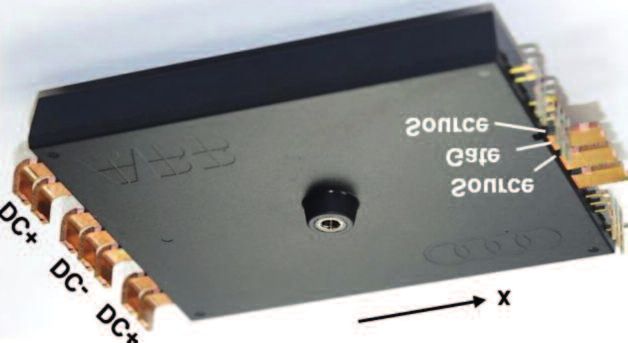
                Half-bridge module design
                The mold modules are designed in half-
                bridge configuration. Two different types
                were developed, a 900 V SiC version for
                screw attachment to the cooler, referred as
                Generation 1 (Gen 1), and a 1200 V SiC
                and Si version for direct cooler bonding,
                referred as Generation 2 (Gen 2), see
                   Figure 2. Both types were designed
                using similar packaging technologies and
                materials.
                   A CTE-matched pin-fin baseplate made
                from AlSiC with a pin-field optimized for
                maximum heat transfer and small
                temperature differences between parallel
                chips is applied to support a
                homogeneous current sharing. A main
                ceramic substrate made from Si 3 N 4 is          Figure 2: 1200 V SiC and Si mold module, Gen 2 design
                bonded to the baseplate by Ag-sintering.
                Semiconductor dies, NTC temperature
                sensor and external per-chip gate resistors
                (only SiC version) are Ag-sintered to the
                main substrate. Top plates made from Cu
                are Ag-sintered to the power
                semiconductor chip top surface to enable
                high-reliability Cu source wire bonds. Al is
                used for the remaining bond wires (gate,
                auxiliary source, substrate-to-substrate
                bonds), see Figure 3. Al2O3 second-level
                substrates are Ag-sintered to the main
                substrate and used for low-inductance
                current routing of the control signals. Cu
                power terminals and auxiliary terminals          Figure 3: Cu source wire bonding on top plate; Al wire bonding for gate, auxiliary source (not shown),
                with press-fit pins are bonded to the main       NTC (bottom left) and interconnects on substrate
                substrate by ultrasonic welding, see
                Figure 4.
                   The module is encapsulated by an
                epoxy-based transfer mold material with
                optimized CTE. A screw thread is
                embedded in the mold compound that
                allows tight fixation of the gate driver board
                and alignment of the modules during
                assembly on the cooler enclosure. The
                substrate and terminal design is optimized
                to achieve symmetric and minimized stray
                inductances and cross-coupling. This is
                achieved by the following design
                approaches, see Figure 5.
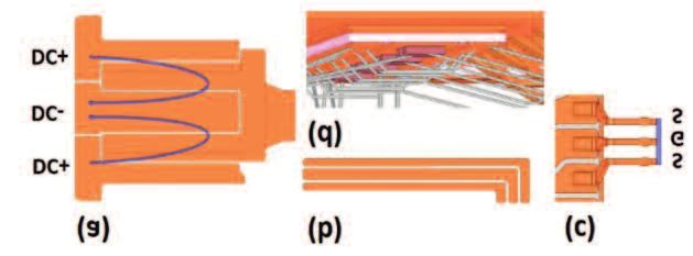
                   The DC commutation loop and the gate
                loops of the half-bridge module are
                arranged in an alternating design so that
                the magnetic fields cancel out to a large        Figure 4: Ultrasonic welded leadframe terminals

www.power-mag.com                                                                                                    Issue 3 2019 Power Electronics Europe
High-Power Module Platform for Automotive Traction Applications - PCIM Europe
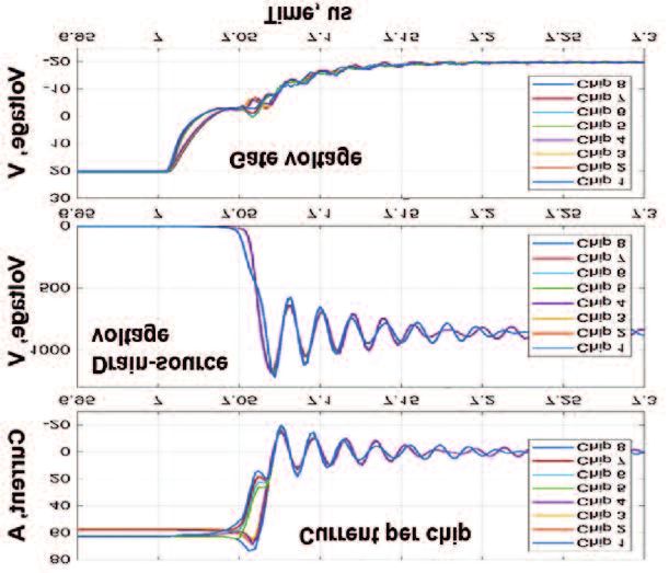
4    AUTOMOTIVE POWER                                                                                                        juergen.schuderer@ch.abb.com

                                                                                                                           modules failed at around 20,000 cycles,
                                                                                                                           the sintered top plate and Cu wire bonded
                                                                                                                           modules were able to reach more than
                                                                                                                           1,000,000 cycles without failure.
                                                                                                                              Among the different ceramic substrate
                                                                                                                           materials commonly used for high-power
                                                                                                                           semiconductor modules, Al/AlN DBA and
                                                                                                                           Cu/Si3N4 AMB substrates have been
                                                                                                                           reported to achieve the highest thermal
                                                                                                                           cycling capabilities. Since Al metallization
                                                                                                                           can be problematic for the ultrasonic
                                                                                                                           welding of Cu terminals, a Si3N4 AMB
                    Figure 5: Alternating current routing for DC+ / DC- current path (a); (b) and (c) Kelvin source and    substrate was selected. In addition, to
                    alternating control signal routing on substrate and terminals; (d) Multilayer signals on second        achieve highest-level reliability when
                    level substrate for minimal magnetic coupling into the gate - source control loop                      targeting high-temperature operation of
                                                                                                                           SiC, a substrate sintering process has been
                                                                                                                           developed.
                                                                                                                              Different baseplate materials (Al, Cu,
                                                                                                                           AlSiC), different bond line thicknesses (20
                                                                                                                           and 40 µm) and different sinter materials
                                                                                                                           (Ag film, Ag preform with metal core) were
                                                                                                                           tested by thermal shock cycling. It turned
                                                                                                                           out that the metal-core sinter preform and
                                                                                                                           an AlSiC baseplate provide best reliability
                                                                                                                           performance. Virtually no delamination of
                                                                                                                           the substrate-to-baseplate attach was
                                                                                                                           found after 1,000 thermal shock cycles
                                                                                                                           both from ⫺40°C to 150°C and from
                                                                                                                           ⫺5°C to 200°C, as well as high-
                                                                                                                           temperature storage tests for 1,000 hours
                                                                                                                           at 200°C and 225°C.

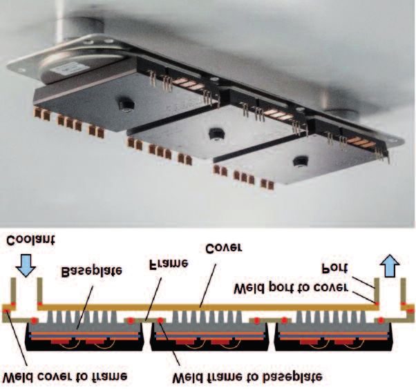
                                                                                                                           Three-phase inverter module and
                                                                                                                           cooler design
                                                                                                                           Water-glycol cooling of power
                                                                                                                           semiconductor modules by means of pin
                                                                                                                           fins has become a preferred way in the
                                                                                                                           thermal management of traction inverters
                                                                                                                           of EVs. Pin fins are either integrated in the
                                                                                                                           module’s baseplate for direct cooling, or
                                                                                                                           are part of a separate, closed cooler, to
                    Figure 6: Simulated switching waveforms for turn-off event based on parasitics extracted at 100 MHz;   which the modules are attached. Whereas
                    high-side chips of Gen 2 SiC module are plotted                                                        the Gen 1 module was designed for screw
                                                                                                                           attach and sealing by an O-ring, the Gen 2
                    to 150°C with a dwell time of 5 minutes at            in the thickness range of 50 – 100 ␮m            module has the full cooler metallurgically
                    each temperature were conducted to verify             showed the best reliability in thermal           bonded to the mold modules.
                    the sinter bond quality. After regular                shock cycling.                                      The cooler assembly concept and final
                    intervals of cycles, the samples were                    Heavy Cu wire bonding has been                inverter module with cooler are shown in
                    inspected using scanning acoustic                     proven to be a superior alternative to Al        Figure 7. The cooler consists of three basic
                    microscopy (SAM) to detect any                        wire bonding with greatly improved power         parts: an Al frame plate that is laser-
                    delamination or degradation of the bond               cycling lifetimes (due to the higher             welded to the mold modules in a first step,
                    layers.                                               electrical and thermal conductivities and        an Al cover plate that is welded to the
                        It is well known that apart from the die          greater mechanical strength of Cu).              frame in a second step, and fluid ports that
                    attach, the chip topside interconnection is           However, the process comes with some             are welded to the cover in a final step.
                    a main limiting factor for the lifetime of            challenges such as high bond forces,                A critical bonding process is the welding
                    power semiconductor devices in active                 narrow process window, influence of top          of the cooler frame to the mold module
                    load cycling conditions. To improve this              plate material, thickness and surface            baseplates. Heat input during this welding
                    issue, sintering a top plate on devices with          properties, as well as accelerated tool          step must be minimized to avoid thermal
                    standard Al metallization and NiAu plating            wear. Thus a 300 ␮m Cu wire bonding              damaging of the modules. Due to this
                    was performed. The top plate acts as a                process was optimized by pull and shear          reason, laser welding has been chosen
                    buffer and allows for Cu wire source                  testing. A special focus was dedicated to        since it is an exceptionally fast process,
                    bonding with superior power cycling                   identify the best compromise for the bond        limiting the temperature rise at the mold
                    lifetime. Different materials (Cu, Mo) and            force to avoid cratering and chip topside        compound side of the power module to
                    thicknesses (50 ␮m, 70 ␮m, 100 ␮m,                    damaging (gate-source short), and to             less than 200°C. Careful process
                    150 ␮m, 200 ␮m) have been tested. As a                achieve sufficiently high shear forces. As a     optimization and well-designed jigs are
                    conclusion, a top plate made of Cu or Mo              result: whereas Al wire bond reference           required to achieve a fluid-tight joint with

Issue 3 2019 Power Electronics Europe                                                                                                         www.power-mag.com
High-Power Module Platform for Automotive Traction Applications - PCIM Europe
juergen.schuderer@ch.abb.com                                                                                           AUTOMOTIVE POWER 5

                                                                                                                         high process repeatability. As an example,
                                                                                                                         material cracks within the welded bond
                                                                                                                         lines may occur that can lead to coolant
                                                                                                                         leakage.

                                                                                                                         Switching losses and rating
                                                                                                                         Double-pulse testing was conducted to
                                                                                                                         determine the switching losses and to
                                                                                                                         assess the power rating to the different
                                                                                                                         module variants. Tests were performed in
                                                                                                                         the temperature range from ⫺20 to 150°C
                                                                                                                         at DC-link voltages up to 850 V, and for
                                                                                                                         currents up to 600 A. Switching waveforms
                                                                                                                         for a Gen 2 SiC hard switching are shown
                                                                                                                         in Figure 8.
                                                                                                                            The measurement was done at a DC-
                                                                                                                         link voltage of 650 V, a current of 400 A, a
                                                                                                                         temperature of 150°C, zero gate resistance
                                                                                                                         (hard switching) and for a stray inductance
                                                                                                                         of the test setup of about 30 nH.
                                                                                                                         Pronounced oscillations results from the
                                                                                                                         fast switching combined with the high stray
                                                                                                                         inductance of the tester. It is therefore
                                                                                                                         important to operate the module in a low
                                                                                                                         inductive inverter environment for optimal
                                                                                                                         performance. In general, however, the
                Figure 7: Cooler schematics and 3-phase power module                                                     traces are quite clean. This is especially
                                                                                                                         important for the critical gate voltage trace
                                                                                                                         (to avoid parasitic turn-on and other
                                                                                                                         issues).
                                                                                                                            Switching losses as measured by
                                                                                                                         double-pulse testing are reported in Table
                                                                                                                         1. SiC losses are given for a gate resistance
                                                                                                                         of 1.7 Ω, and for a hard-switched
                                                                                                                         configuration with 0 Ω. In addition, Gen 2
                                                                                                                         Si losses and Gen 1 SiC losses (at a DC-
                                                                                                                         link of 400 V) are given. Note that tests
                                                                                                                         were performed with different double-
                                                                                                                         pulse setups and gate drivers which makes
                                                                                                                         a direct comparison difficult.

                                                                                                                         Conclusions
                                                                                                                         An automotive SiC and Si power module
                                                                                                                         platform targeting inverter classes of
                                                                                                                         premium and commercial EVs in the power
                                                                                                                         range of 150 – 350 kW was presented.
                                                                                                                         Mold modules are bonded to an integrated
                                                                                                                         cooler enclosure that allows for a compact,
                                                                                                                         and screw-less inverter design. High-
                                                                                                                         reliability packaging technologies are
                                                                                                                         employed enabling operation up to 200°C
                                                                                                                         junction temperature.

                                                                                                                         Literature
                                                                                                                            “High-Power SiC and Si Module
                Figure 8: Turn-on (top) and turn-off (bottom) switching waveforms of SiC Gen 2 module at 25°C; blue:     Platform for Automotive Traction
                current, red: voltage, green: gate voltage                                                               Inverter”, Jürgen Schuderer, BPA
                                                                                                                         Winner, ABB Corporate Research,
                                                                                                                         Switzerland, and Andreas Apelsmeier,
                                                                                                                         AUDI AG, Germany, PCIM Europe 2019
                                                                                                                         Proceedings

                                                                                                      LEFT Table 1: Switching losses measured by double-pulse testing;
                                                                                                      Gen 2: U = 800 V, I = 400 A, Gen 1: U = 400 V, I = 400 A; T = 100 -
                                                                                                      150 °C; RG = total chip-external gate resistance

www.power-mag.com                                                                                                       Issue 3 2019 Power Electronics Europe
High-Power Module Platform for Automotive Traction Applications - PCIM Europe
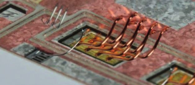
6    AUTOMOTIVE POWER                  juergen.schuderer@ch.abb.com

Issue 3 2019 Power Electronics Europe             www.power-mag.com
High-Power Module Platform for Automotive Traction Applications - PCIM Europe
juergen.schuderer@ch.abb.com   AUTOMOTIVE POWER 7

www.power-mag.com              Issue 3 2019 Power Electronics Europe
High-Power Module Platform for Automotive Traction Applications - PCIM Europe
8    AUTOMOTIVE POWER                  juergen.schuderer@ch.abb.com

Issue 3 2019 Power Electronics Europe             www.power-mag.com
High-Power Module Platform for Automotive Traction Applications - PCIM Europe
juergen.schuderer@ch.abb.com   AUTOMOTIVE POWER 9

www.power-mag.com              Issue 3 2019 Power Electronics Europe
You can also read