High-speed femtosecond laser plasmonic lithography and reduction of graphene oxide for anisotropic photoresponse - Nature
←
→
Page content transcription
If your browser does not render page correctly, please read the page content below
Zou et al. Light: Science & Applications (2020)9:69                                                                                         Official journal of the CIOMP 2047-7538
                                    https://doi.org/10.1038/s41377-020-0311-2                                                                                                                        www.nature.com/lsa

                                     ARTICLE                                                                                                                                                    Open Access

                                    High-speed femtosecond laser plasmonic
                                    lithography and reduction of graphene oxide for
                                    anisotropic photoresponse
                                    Tingting Zou1,2, Bo Zhao1,3, Wei Xin                           1
                                                                                                     , Ye Wang1,2, Bin Wang1,2, Xin Zheng1,2, Hongbo Xie1,2, Zhiyu Zhang4,
                                    Jianjun Yang1 and Chunlei Guo1,5

                                      Abstract
                                      Micro/nanoprocessing of graphene surfaces has attracted significant interest for both science and applications due to
                                      its effective modulation of material properties, which, however, is usually restricted by the disadvantages of the current
                                      fabrication methods. Here, by exploiting cylindrical focusing of a femtosecond laser on graphene oxide (GO) films, we
                                      successfully produce uniform subwavelength grating structures at high speed along with a simultaneous in situ
                                      photoreduction process. Strikingly, the well-defined structures feature orientations parallel to the laser polarization and
                                      significant robustness against distinct perturbations. The proposed model and simulations reveal that the structure
                                      formation is based on the transverse electric (TE) surface plasmons triggered by the gradient reduction of the GO film
                                      from its surface to the interior, which eventually results in interference intensity fringes and spatially periodic
                                      interactions. Further experiments prove that such a regular structured surface can cause enhanced optical absorption
                                      (>20%) and an anisotropic photoresponse (~0.46 ratio) for the reduced GO film. Our work not only provides new
                  1234567890():,;
1234567890():,;
                  1234567890():,;
1234567890():,;

                                      insights into understanding the laser-GO interaction but also lays a solid foundation for practical usage of
                                      femtosecond laser plasmonic lithography, with the prospect of expansion to other two-dimensional materials for
                                      novel device applications.

                                    Introduction                                                                                        electrons in plasmonic systems, which enable the pat-
                                      Graphene analogs, such as graphene oxide (GO) and its                                             terned materials to have great vitality in numerous
                                    reduced forms (rGO), are fascinating carbon materials                                               research areas, such as optical field regulation, optoelec-
                                    due to the complementary properties endowed by the sp3-                                             tronics, energy harvesting and chemo/biosensing5–8.
                                    sp2 interconversion, revealing the substitutability and                                               Effective implementation of many techniques, including
                                    potential for industrialization of integrated graphene                                              directed assembly, nanoimprinting, and lithography
                                    devices1,2. Reasonable micro/nanostructural design of GO                                            combined with electron-beam etching, thermochemical,
                                    and rGO to control the energy band gap and surface                                                  and scanning probe technologies, for fabricating struc-
                                    chemical activity is important for developing strategic                                             tures with high spatial resolution has been demonstrated,
                                    applications3,4. In particular, uniform periodic structures                                         but these techniques are time consuming, costly, or lack
                                    over large areas exhibit attractive collective oscillations of                                      versatility9–13. In contrast, femtosecond laser-based pro-
                                                                                                                                        cessing, associated with the benefits of being facile,
                                                                                                                                        maskless, and efficient, is a qualified candidate for
                                    Correspondence: Wei Xin (weixin@ciomp.ac.cn) or Jianjun Yang
                                    (jjyang@ciomp.ac.cn) or Chunlei Guo (chunlei.guo@rochester.edu)                                     industrial development14, and recently, it has been applied
                                    1
                                      State Key Laboratory of Applied Optics, Changchun Institute of Optics, Fine                       in the micro/nanomanufacturing of graphene analogs,
                                    Mechanics and Physics, Chinese Academy of Sciences, 130033 Changchun, China
                                    2                                                                                                   such as typical patterning of GO films15. Due to the
                                      Center of Materials Science and Optoelectronics Engineering, University of Chinese
                                    Academy of Sciences, 100049 Beijing, China                                                          nonthermal and thermal effects during this processing,
                                    Full list of author information is available at the end of the article

                                    © The Author(s) 2020
                                                        Open Access This article is licensed under a Creative Commons Attribution 4.0 International License, which permits use, sharing, adaptation, distribution and reproduction
                                                        in any medium or format, as long as you give appropriate credit to the original author(s) and the source, provide a link to the Creative Commons license, and indicate if
                                    changes were made. The images or other third party material in this article are included in the article’s Creative Commons license, unless indicated otherwise in a credit line to the material. If
                                    material is not included in the article’s Creative Commons license and your intended use is not permitted by statutory regulation or exceeds the permitted use, you will need to obtain
                                    permission directly from the copyright holder. To view a copy of this license, visit http://creativecommons.org/licenses/by/4.0/.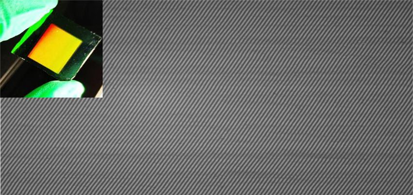
Zou et al. Light: Science & Applications (2020)9:69                                                             Page 2 of 11

simultaneous in situ photoreduction can be realized just        interaction and exhibits unique characteristics, such as
by removing the oxygen-containing functional groups of          high efficiency and strong robustness against a range of
GO, which leads to controllability of GO’s morphology           perturbations. The simultaneous occurrence of the large-
and reduction degree by changing the duration, intensity,       area grating structure formation and photoreduction
or wavelength of the laser irradiation15–17. At present, the    processes greatly simplifies the work procedures. For
most commonly adopted technologies for photoreduction           example, compared to laser direct writing adopting the
of GO materials by femtosecond lasers are based on direct       same incident laser parameters, the FPL strategy takes
writing and beam interference18,19. The difficulty faced in      only ~1/14,000 of the time to process a centimeter-sized
the former case is the slow processing speed, while the         sample (1 × 1.2 cm2). Meanwhile, due to the possible
latter’s greatest problem is the poor splicing quality of the   nonlinear optical property22, the FPL strategy induces an
micro/nanostructures formed at the joint of the moving          obvious “self-repairing” phenomenon, which can effec-
light spots, especially when a large area must be pro-          tively guarantee the processing quality. We can prepare
cessed. Meanwhile, confined by the optical diffraction           rGO-LIPSS films on different substrates and non-
limit, the maximum processing accuracy of both common           destructively transfer them onto other substrates. In
methods can only be comparable to the incident                  addition, as another new phenomenon, the processed
wavelength.                                                     grating structure strictly parallel to the TE polarization
   Here, by utilizing a new strategy of femtosecond laser       state of the incident light should also be noted. This
processing, so-called femtosecond laser plasmonic litho-        implies that complex topography preparation is feasible
graphy (FPL), we present high-speed, large-area micro/          by changing only the polarization23.
nanomanufacturing, and photoreduction of GO films                   All the abovementioned advantages of the FPL strategy
(~140 nm) on a silicon substrate (300 nm SiO2/Si). Peri-        are conducive to flexible and rapid preparation of high-
odic grating structures with high regularity (~680 nm           quality micro/nanostructures on the surface of GO.
period) can be induced on the surface of the reduced GO         Because the process contains no assistant operations, such
film even at a centimeter scale. Although the first obser-        as chemical etching, the properties of the graphene
vation of laser-induced periodic surface structures             material are retained. As a matter of fact, through mod-
(LIPSSs) can be traced back to 50 years ago20,21, whose         ulation of the GO reduction degree and structural design
universal property has been confirmed for various mate-          of the rGO surface, we can change the properties of the
rials, including metals, semiconductors, and insulators,        rGO film, which allows us to further apply the material to
the low structural quality is obviously one of the most         optoelectronic applications. For example, the periodic
important factors restricting their further application.        grating structures have obvious optical trapping and
Flexible and controllable energy deposition to achieve          grating coupling effects, which enhance the light absorp-
practical structural fabrication in the subwavelength range     tion by ~20% compared with the smooth surface5, and the
through the FPL strategy has only been recognized in            light-active property of rGO also makes it suitable for
recent years22–26. The key factor in this process is the        realizing a photoresponse over a wide spectrum31–33. Our
lossy and reversible nature of the plasma waves, which          devices can realize stable photoresponsivity (R ~ 0.7 mA
allows us to obtain feedback at local positions and in turn     W−1) even when exposed to light with low power
control the energy distribution to achieve the formation of     (0.1 mW). This is numerically comparable to the response
regular structures22,27. In our experiments, we demon-          of samples obtained by other reduction methods (e.g.,
strate that the laser-induced gradient reduction of GO          chemical and thermal) but is much larger than that of
film from its surface to the interior plays a key role, which    typical photoreduced samples31–33. In addition, the dif-
produces an inhomogeneous slab with the maximum                 ferent reduction degrees of rGO along and vertical to the
dielectric permittivity (DP) at the surface and a smaller       grating structures lead to its in-plane effective refractive
DP at deeper thicknesses that allows excitation of TE-          indexes being different in the two directions, which in
mode surface plasmons (TE-SPs)28–30. The further inter-         turn lays the foundation for the anisotropic response of
ference between the incident light and the excited TE-SPs       rGO photodetectors34. The conductivity of our devices
modulates the laser energy distribution, leading to a           has an anisotropy ratio of 0.46, which is even larger than
periodic LIPSS with orientation parallel to the laser           that of some natural anisotropic crystals35,36. It should be
polarization direction23,27. Notably, the idea of TE-SP         noted that this is the first time that we apply the FPL
excitation is newly proposed in the application of the FPL      strategy to the practical application of graphene analogs,
strategy, which obviously helps us understand the similar       not just to the usage of grating structures25,26. Our work
processing of related materials.                                combines experimental exploration with the in-depth
   Different from previous reports about the laser pro-         theoretical understanding of high-speed micro/nano-
cessing of graphene materials, our manufacturing process        patterning of regular rGO-LIPSS, which not only benefits
has diverse physical mechanisms during the laser–rGO            fundamental physics but also facilitates the practical
Zou et al. Light: Science & Applications (2020)9:69 Page 3 of 11
development of graphene analogs on the industrial width aspect ratio as large as approximately 800. The
scale37–39. grating formation is determined by tuning the scanning
speed and the laser energy fluence within wide ranges of
Results 0.5–200 μm s−1 and 25.6–140.2 mJ cm−2, respectively.
High-speed femtosecond laser plasmonic patterning of The typical experimental parameters were fixed as 10 μm
graphene oxide film s−1 and 95.6 mJ cm−2 here, indicating that the number of
The formation of rGO gratings on a rigid substrate is spatially overlapping laser pulses is approximately 1200
the basis for further complex operations, which also within the beam spot area or that the irradiation of almost
exhibits potential application in optoelectronics, such as 100 laser pulses accumulates within a 1 μm distance.
in the fabrication of tuneable terahertz and hyperbolic Details can be seen in the Materials and methods section
metamaterial devices5,7. Here, GO was prepared using the and Supplementary Information (SI) S1, S2.
modified Hummer’s method40,41. After being fully dis- Figure 1b presents an example of the grating structure
solved in deionized water, a uniform film with an obtained using the aforementioned approach, where a
~140 nm thickness was spin-coated on the surface of a large scanning area with a 10 × 12 mm2 coverage and a
commercial silicon slice (300 nm SiO2). Large-area peri- regular period of ~680 nm can be seen in the photograph
odic grating structures were fabricated on the GO film by (insert) and scanning electron microscopy (SEM, Phe-
scanning the fs laser irradiation (Spectra Physics, 40 fs, nom) images. The detailed topology with plentiful hier-
800 nm, 1 kHz) through a cylindrical lens (focal length of archical nanostructures on the surface is shown in Fig. 1c.
50 mm) in ambient air, as shown in Fig. 1a. Because a laser In contrast to the traditional laser direct writing method,
focused by a cylindrical lens is restricted only in one in which large-area processing often requires multiple
dimension, the focal beam spot on the GO film presents a scribing of lines, our technology operated here exhibits a
line profile with measured length and width of ~10 mm much improved efficiency. Using the same parameters in
and ~12.37 μm, respectively, resulting in a length-to- terms of the laser fluence, pulse repetition rate and
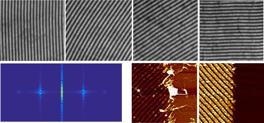
a b 1c
800 nm, 40 fs, 1 kHz m
l lens
Cylindrica
E
S
S θ
rGO Z
E 10 μm
SiO 2 Y
Si X
d
c θ = 0° θ = 30° θ = 60° θ = 90°
5 μm
e f ~65 nm
FFT ~40 nm
±δ
~35 nm
1 μm
2 μm
Fig. 1 High-speed micro/nanograting processing of GO film using the FPL strategy and morphology characterizations. a Schematic of
grating processing of a GO film using cylindrical focusing of femtosecond laser pulses. The sample (GO/SiO2/Si) is mounted on a three-dimensional
(3D) translation stage. The cyan and red arrows represent the directions of the sample scanning (S) and the linear polarization (E) of the laser,
respectively. b Photograph (insert) and SEM image of the large-area (10 × 12mm2) rGO-LIPSS. The uniform structural color (yellow) shows the spatially
regular distribution of structures, where θ represents the angle between S and E. It can be precisely adjusted by a half-wave plate and a Glan-Taylor
prism. c High-resolution SEM image of the LIPSS corresponding to the position in the white box in b. d Observed parallel dependence between the
grating orientation and the laser polarization direction. e 2D-FFT spectrum suggesting that the period along with its standard deviation (δ) is Λ ± δ =
680 ± 18nm. f AFM images of the rGO-LIPSS on a Si/SiO2 substrate. The film thickness is decreased by ~40 nm as a whole, and the depth between the
ridges and valleys is ~65 nm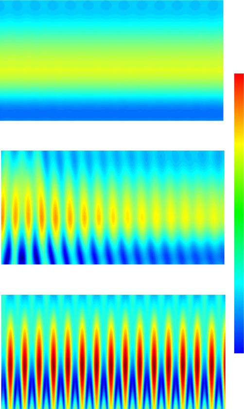
Zou et al. Light: Science & Applications (2020)9:69                                                              Page 4 of 11

scanning speed, the time consumption here can be                 beam spot. Because the deeper morphologies represent
decreased by at least 4 orders of magnitude when tex-            the regions of stronger laser–material interaction, the
turing a surface area of 10 × 12 mm2. In addition, different     formation of the grating patterns physically indicates the
from the observations of a low-spatial-frequency LIPSS           occurrence of a spatially periodic distribution of the laser
reported on other materials23–27, the spatial orientation of     intensity. In other words, during the scanning (or pulse
our achieved structures is shown to be strictly parallel to      overlapping) process, the incident laser intensity with a
the direction of the linear polarization of the incident laser   smooth Gaussian distribution on the surface is readily
(Fig. 1d). This feature also ensures flexible patterning by       transformed into multiple strong-and-weak energy fringes
changing the scanning direction and laser polarization.          with a certain period, which results in selective laser
However, to obtain higher quality structures, the two            interactions with the film. By increasing the laser fluence,
directions are recommended to be consistent42. Figure 1e         we can find that the surface morphology and the depth of
shows a typical 2D fast Fourier transform (2D-FFT)               the LIPSS change. Although this processing will be
spectrum obtained from the SEM image (θ = 0°). The               accompanied by laser ablation, a higher intensity of the
calculated structure period is approximately Λ ± δ =             laser is obviously required to reach the threshold43. The
680 ± 18 nm, with δ being the standard deviation. The            detailed variation tendency can be seen in SI S4.
regular distribution of the spatial frequency means highly          This laser-induced periodic photoreduction was more
ordered fabrication of the surface structures. Moreover,         intuitively confirmed by the spatial distribution of the
we found that the period of the structures is slightly less      chemical composition measured using energy dispersive
than the laser wavelength and remains almost invariable          spectrometry (EDS, Phenom Prox). Figure 2a shows the
with the pulse shot number and the energy fluence. This           content maps of the different elements of carbon (C+)
phenomenon may be due to the commonality of carbon               and oxygen (O−) on the LIPSS of the film. Clearly, the
materials, which has been reported earlier27. For the dif-       spatial distribution patterns of the chemical elements are
ferent processing parameters, the variation tendency of          highly consistent with the grating structures. With the
the structure period can be seen in SI S3. The dynamic           geometric undulations of the rGO-LIPSS, we can find that
process of grating structure formation in a large area can       the elemental constituents are different at the ridge and
be found in Supplementary Movies (SM) SM1, SM2, and              valley positions/localizations. Here, the grating structure
SM3.                                                             period is approximately Λ = 680 nm, while the structure
                                                                 depth is only approximately d = 65 nm, leading to a sur-
Periodic photoreduction of graphene oxide film                    face fluctuation with a width-to-depth ratio of approxi-
   Here, along with the micro/nanopatterning process, it         mately 5:1. Such a large aspect ratio can enable us to
should be emphasized that the GO film is simultaneously           consider that the surface morphology has no influence on
photoreduced, indicating the generation of an rGO-               the EDS signal collection; the obtained periodic bright-
LIPSS. Because the oxygen-containing functional groups           dark EDS patterns of the rGO-LIPSS are mainly caused by
are readily removed from the surface region by both              the uneven degree of the photoreduction process. To
nonthermal (two-photon absorption, for instance) and             clarify the above deduction, we also characterized the film
thermal photoreduction effects, the surface morphology           by measuring the Raman spectra (Horiba, Jobin Yvon)
of GO will accordingly change during the laser irradia-          within a wavenumber range from 800 to 3500 cm−1 under
tion15,43. Generally, the thickness of the GO film decrea-        excitation by a continuous 532 nm laser. The repre-
ses after photoreduction15, so a preliminary judgment of         sentative sp2 vibration of atoms and in-plane disturbance
the reduction state of the GO sample can be made based           of disordered graphite generally occur in carbon materi-
on just its thickness comparison before and after laser          als, which correspond to the G peak at ~1594 cm−1 and D
irradiation.                                                     peak at 1351 cm−1, respectively38. Another peak occurring
   In our experiment, two phenomena need to be noted:            at ~2920 cm−1, which is the 2D band that indicates the
first, in the entire illuminated area, an overall decrease of     atom stacking morphology of multilayer graphene, can
~40 nm in the film thickness can be observed. Second, the         also be observed. The D/G intensity ratio is widely used to
thickness difference between the ridges and valleys is           analyse the reduction degree of GO. The smaller this ratio
~65 nm for the grating structures, with no damage to the         is, the higher the reduction degree.
silicon substrate during the laser processing, as shown by          Figure 2b shows the Raman spectra measured for the
the atomic force microscopy (AFM, Bruker, Billerica)             GO film without any laser treatment and for the ridge and
images in Fig. 1f. For the first phenomenon, we believe           valley positions/localizations on the rGO-LIPSS. Regard-
that it is the result of the GO surface being reduced as a       less of the case, three typical peaks (D, G, and 2D) can
whole, whereas for the second one, we infer that it is           always be seen, whereas the D/G intensity ratios are
caused by the change in the energy profile of the laser           slightly different. Compared to the value of ID/IG = 1.067
Zou et al. Light: Science & Applications (2020)9:69 Page 5 of 11
a SEM b GO
C+ O– D G
rGO-LIPSS-ridge
ridge rGO-LIPSS-valley
Intensity (a.u.)
valley
ID/IG = 1.067 2D
ID/IG = 0.953
5 μm ID/IG = 0.928
1000 1500 2000 2500 3000 3500
–1
Raman shift (cm )
c 10 d
D G 2D
7.5
Position (μm)
5
2.5
1μm
0
800 1200 1600 2000 2400 2800 3200 SEM D G 2D D/G
Raman shift (cm–1)
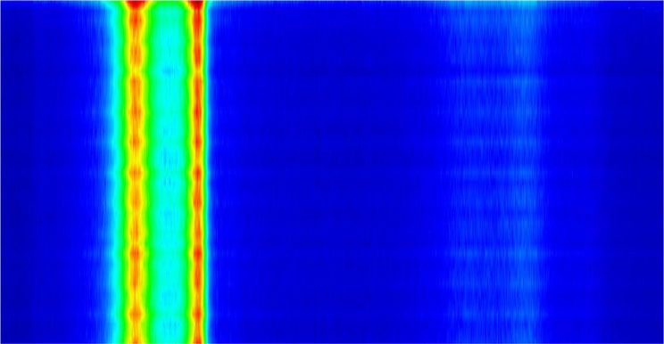
Fig. 2 Spatially periodic photoreduction of GO film. a SEM image of the rGO-LIPSS and corresponding EDS images of carbon (C+) and oxygen (O
−) elements. b Comparison of the Raman spectra for the GO film and the ridge and valley positions of the rGO-LIPSS. Both the ridge and valley
positions are indicated in a. c Measured spatial distribution of Raman spectra along the direction (white arrow shown in a and d) perpendicular to
the grating orientation. d Measured spatial distributions of three different Raman peaks
for the pristine GO film, the values at the ridge (0.953) we can use a semiphenomenological theoretical model for
and valley (0.928) positions of the rGO-LIPSS decrease, guidance. The nonthermal or thermal photoreduction
which suggests C–C bond recovery of the material and its effects play a crucial role during the fs laser irradiation of
gradual graphitization44,45. The ID/IG values for different GO film17. With the gradual accumulation of laser pulses
samples and at different locations are the average results on the material surface, the degree of reduction can vary
from multiple tests (Table S2), and the trend can be from the surface to the interior. This results in an inho-
clearly illustrated by the spatially resolved Raman inten- mogeneous DP distribution along the depth, whose gra-
sity distribution of the rGO-LIPSS samples. When the dually decreasing values meet the basic conditions for the
sample was scanned perpendicular to the LIPSS orienta- excitation of the TE-SP wave (Fig. 3a, upper)28,29. Con-
tion, we found that the variations in the Raman peak sequently, the TE-SP wave is excited and interferes with
intensities well matched the topographic undulations of the incident light to form periodic energy deposition
the rGO-LIPSS (Fig. 2c). Furthermore, when we per- fringes. Then, spatially periodic reduction and ablation of
formed an area-scanning measurement, periodic dis- the GO surface occur, and the positive feedback further
tributions of the different Raman peaks are evidently promotes the excitation of TE-SPs. More importantly, the
shown (Fig. 2d). Therefore, we can conclude that during interference fringe intensity at any point of the film is an
rGO-LIPSS formation, the GO film is not only photo- integral effect of the incident and scattered light over a
reduced but also has different degrees of reduction in the large area, so-called nonlocal feedback formation. Due to
ridge and valley regions. To quantitatively analyse the the high carrier concentrations in the graphene material,
reduction, both X-ray photoelectron spectroscopy (XPS, the excited TE-SP wave can propagate a long distance,
Thermo Escalab 250Xi) and X-ray diffraction (XRD, and the feedback is strong enough to regulate the energy
Rigaku SmartLab) were employed for the measurement. deposition (Fig. 3a, middle)46. Therefore, when the fs laser
Detailed descriptions can be found in SI S5. spot is scanned in a certain direction, the partially over-
lapping laser energy distributions will duplicate the
Simulation analysis of plasmonic formation on graphene existing periodic patterns onto the new laser-exposed
oxide film positions step by step, resulting in large-area uniform
The formation of the rGO-LIPSS is a complex process formation of the LIPSS (Fig. 3a, bottom). This kind of
including miscellaneous physical mechanisms, whereas nonlocal feedback mechanism presents excellent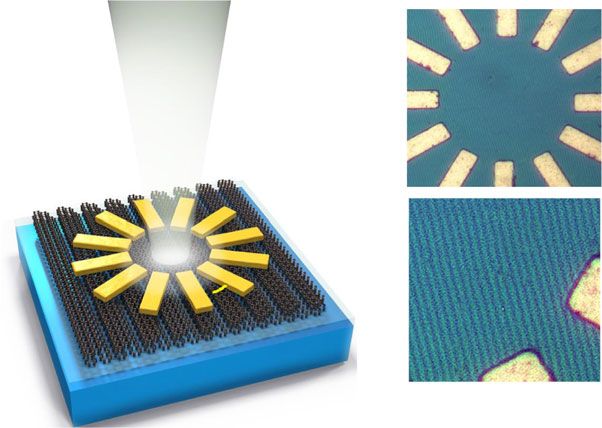
Zou et al. Light: Science & Applications (2020)9:69 Page 6 of 11
a b c 300
800 nm/ 40 fs/ TE polarization |E|
10 λs1 = ~660 nm 200
λs2 = ~700 nm
q (rad μm–1)
TE-SP 100
9
b = –0.101 1
Z rGO-GO b = –0.205 0
ε(z) L 8 b = –0.39
140 nm b = –1.01 –100
SiO2 300 nm b = –0.88
0 2 4 6 8 10
Si 500 μm 7 λ0 = 800 nm 300
|E|
6.8 7.2 7.6 8.0 200
z (nm)
–1
ω/c (rad μm )
E 100
d 0
rGO-GO
z a 1.0 SiO2
–100
x < 140 nm 0 2 4 6 8 10
SiO2 300 nm 300
| Ex | (a.u.)
500 μm 0.75 |E|
Si
200
Air
d D 0.5 rGO film 100 0
rGO w Λ n1 n2
0
SiO2 300 nm
Si 500 μm –100
0.0 0.1 0.2 0.3
0 2 4 6 8 10
z (μm)
x (μm)
Fig. 3 Simulation analysis of the plasmonic formation on GO film. a Schematic diagram of rGO-LIPSS formation. Upper: schematic of the TE-SP
excitation at the rGO-air interface. The unusual TE-SP wave is excited following the gradient change in the DP distribution (ε(z)) from the surface to
the interior of the rGO/GO sample (along the z direction) after femtosecond laser irradiation. “L” represents the initial thickness of the GO film before
processing. Middle: Detailed description of TE-SP excitation. “a” is the thickness of the inhomogeneous rGO film. Bottom: Formation of the rGO-LIPSS
after processing. “Λ” is the center-to-center distance between two grooves, and “w” and “d” represent the width and depth of the grooves,
respectively. “D” is the final thickness of the rGO film after processing. “n1” and “n2” are the refractive indexes at the ridge and valley positions,
respectively. b Dispersion relation of the TE-SP wave for different inhomogeneity strengths (b) and carrier densities (N). The dispersion of light in
vacuum is shown as the black line. λ0 and λs represent the wavelengths of the incident light and TE-SP wave, respectively. c Simulated intensity
fringes of the E field distribution without (upper) and with (middle, bottom) phase matching using the FDTD methods. The depths of the initial and
terminal ripples are defined as 20 and 65nm, respectively. d Calculated spatial profile of the E field intensity for the inhomogeneous film
robustness against disturbances, which makes rGO-LIPSS should satisfy the following equation:
formation more flexible and extensible22. Although
grating-like structures have already been fabricated by ωa2 1 1 ∂Kρ ðsuÞ
2
other methods, such as laser direct writing and beam ðqs aÞ2 ¼ þ þ ð1Þ
c 2 Kρ ðsÞ ∂u
interference5,19, both the efficiency and robustness of our u¼1
FPL strategy are undoubtedly highlights. More details on
the flexible sample processing can be found in SI S6 and where qs is the wavevector of the TE-SP wave and c and ω
S7 and SM S4. are the speed and frequency of incident light, respectively.
To further elucidate the formation of the rGO-LIPSS, a Kρ(su) is the Bessel function of the second kind, which
28
simplifies the calculation of the Helmholtz equation .
physical model is introduced as follows: first, we assume 2 ωa 2 ω 2
that the degree of reduction of the GO film gradually Here, u¼1þ a , Dz
s ¼ ðqs aÞ εL c þ εL cpa
2
ω a2
1 1b , ρ2 ¼ εbL cp þ 14, and ω2p ¼ 4πe
2N
εL meff . ωp is defined as
0
decreases with the material depth (z direction in Fig. 3a).
Starting from the electromagnetic field theory, the com- the inherent plasma frequency of bulk rGO material
plex amplitude of the electric (E) field distribution near associated with carrier density N0 at the air-rGO interface
the air-rGO interface satisfies the Helmholtz equation. (z = D), and meff is the carrier effective mass. εL is the
Considering the depth-dependent influence of the inci- frequency-independent part of the DP of the film. a (>0) is
dent laser beam on the rGO film, ε(z) is defined as the z- the thickness of the inhomogeneous rGO layer, and the
dependent DP and can be derived from the carrier density dimensionless parameter b describes the strength of the
distribution (N) using the Drude model. After introducing inhomogeneity. Subsequent studies found that the specific
ε(z) into the Helmholtz equation, the E field in the rGO form of the z-dependent gradient of the carrier density in
film can be solved. Considering the continuity boundary the rGO film has little influence on the results of the
condition at the air-rGO interface, the dispersion relation E field distribution. Detailed information can be found in
of the TE-SP wave propagating along the rGO surface SI S8.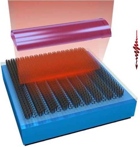
Zou et al. Light: Science & Applications (2020)9:69                                                           Page 7 of 11

   Dispersion relation curves were obtained, as shown in       This enhanced optical absorption causes an increase in
Fig. 3b, which illustrates the possibility of the generation   the temperature of the samples, which in turn promotes
of a collective oscillation of pseudo-surface currents. The    the photoelectric conversion due to the excellent photo-
values of N0 and b satisfying the TE-SP wave excitation        thermoelectric and bolometric properties of graphene50.
have a wide range. They are mainly limited by the DP           Meanwhile, considering that the different reduction states
variation of the GO film, the change range of the plasma        along the parallel and vertical directions of the LIPSS may
frequency (ω > ωp), and the wavelength of the TE-SP wave       result in differentiated photoresponses, it is evident that
in the measurements (qs ~ 8.98–9.52 rad μm−1). Other           the structured rGO samples are a promising material for
relevant parameters are shown in Tables S1 and SI S9.          anisotropic photoelectric devices34–36.
   To support the experimental data, simulations were             The schematic architecture of an on-chip photodetector
carried out to determine the E field distribution using the     is shown in Fig. 4a. Twelve electrodes (50 nm gold) spaced
finite difference time domain (FDTD) method. By intro-          at an angle of 30° were fabricated on the rGO film. The
ducing four equally spaced grooves as a phase matching         direction parallel to the LIPSS orientation is marked as a
excitation, coupling of incident light into the TE-SP wave     reference (the red arrow), and its anti-clockwise angle
excitation can be efficiently realized, as compared in Fig.     with the alignment direction (the green arrow) of the
3c (upper and middle)23,27. The TE-SP wave propagates          oppositely placed electrode pairs is marked as α. Each pair
on the surface of the inhomogeneous film and further            of electrodes was used as the source and the drain. Figure
induces grating structures. As the grating depth increases,    4b presents a comparison of the light absorption of GO
the excitation efficiency of the TE-SP wave is improved,        films before and after the laser processing. Within a wide
and the spatial regularity of the E field is also increased     spectral range from the visible to infrared (380–2200 nm),
(Fig. 3c bottom). Figure 3d shows the spatial profile of the    the structured rGO film surface exhibits light absorption
E field intensity for the TE-SP wave across the film,            with an enhancement of ~20%. The corresponding
wherein the E field value extends from the air into the         infrared image shows that the temperature in the laser
interior of the rGO film, with the maximum intensity            processed area increases by more than 10 °C (Fig. 4c). As a
occurring at the air–rGO interface.                            comparison, the temperature response of a thermally
   Here, there are still several problems that need to be      reduced sample was also investigated. The results show
further emphasized. First, the z-dependent gradient dis-       that the change in temperature is not significant if the
tribution of the DP plays an essential role in the structure   reduction of GO only sample is considered (
Zou et al. Light: Science & Applications (2020)9:69 Page 8 of 11
a b 80 c 36
α
GO rGO
rGO-LIPSS
Temperature (°C)
60 31
GO
A%
40
26
20
rGO
Au
α 21
rGO Z
Y
0
SiO 2 400 800 1200 1600 2000 GO
X
Si Wavelength (nm) 16
d e 0.8 f 0.8 1 mW
90° 1.2
Vds = 5 V tr ≈ 5.8 s
20 0.6
0.12
135° 45° tf ≈ 5.5 s
Conductance (μS) 0.4 Off
15 0.9 On
0.4
Current (mA)
10
R (mA/W)
0° 0.0
PC (μA)
PC (μA)
180°
0.08 0 10 20 30 40 50
0.6
0.2 0.8
0.104
0.4
0° 30°
60° 90°
0.00 0.0
0.3
0 1 2 3 4 5 0.3 0.6 0.9 20 50 80 110
Voltage (V) P (mW) Times (s)
Fig. 4 Photoelectric response of the rGO samples with the rGO-LIPSS. a Schematic diagram (left) and photographs (right) of the angle-resolved
photoelectric measurement of rGO samples. The top-down materials of the samples are gold electrodes (50nm), rGO-LIPSS (~100nm), SiO2 film
(300nm) and Si substrate. α represents the angle between the alignment of the electrode pair used for measurement (the green arrow) and the
reference position (the red arrow). Here, there is a deviation of ~10° between the processing direction of the LIPSS and the ideal case. The scale bars
are 20 μm (top) and 5 μm (bottom). b, c Light absorption and corresponding infrared images at the positions of the GO film and the rGO-LIPSS. The
scale bars in c are 500 μm. d α-dependent I–V curves (main) and conductance (inset) of rGO samples. e Photoresponsivity (R) and photocurrent (PC)
of rGO samples under irradiation by LED white light (OPTO SIGMA, SLA-100). f Temporal photoresponse of rGO samples under 1mW irradiation
photoreduced samples31–33. However, the photoresponse polarization direction of the incident light increases the
speed of our samples is relatively slow, as shown by the degrees of freedom for us to control the morphology
temporal measurement in Fig. 4f. The rise and fall times formation. By adjusting the time delay between laser pulse
are 5.8 s and 5.5 s, respectively. The reason is that the rGO trains, we can further manipulate the laser processing to
film surface contains plentiful oxygen-containing func- achieve more complex topography51. The FPL strategy
tional groups and micro/nanostructures that greatly has also been proven to be capable of breaking the dif-
increase the specific surface area, which hinders the fraction limit by applying suitable experimental para-
electrical conductivity. The bolometric and photo- meters21,47. Apart from this, we should also emphasize
thermoelectric effects, rather than the photovoltaic effect, that the phenomenon here is different from others,
may play key roles here. although similar works have been covered in previous
reports23–27. The spatial orientation of the grating is
Discussion parallel rather than perpendicular to the polarization
It is of great practical significance to use the FPL direction of the incident light, leading to a completely
strategy to realize high-speed, large-area, and uniform different analysis of the laser-matter interaction. This lays
micro/nanofabrication on the surface of 2D materials, the foundation for us to enrich the physical mechanisms
whereas both the theoretical and experimental explora- of and to fully understand the FPL processing procedure.
tions of this method are still in their infancy. Compared In addition, we should also note that the design and
with existing femtosecond laser processing technologies, processing of the micro/nanostructures on the surface of
such as direct writing and beam interference, the FPL the sample are the basis of the early stage, whose final
strategy is mainly based on incident light-SP interference purpose is to optimize the properties of materials for
and exhibits nonlinear optical characteristics, so it has further application. Through the characterizations and
superiorities of higher efficiency and stronger robustness photoelectric measurements of the rGO-LIPSS, the sam-
against a range of perturbations. Moreover, notably, it ples processed by our FPL strategy are proven to retain
should present potential for surface processing with most of the properties of graphene and become even
flexible controllability and high accuracy. The corre- better in some aspects, such as higher light absorption and
spondence between the LIPSS orientation and the an anisotropic photoresponse. Therefore, we should fully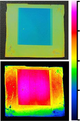
Zou et al. Light: Science & Applications (2020)9:69                                                                        Page 9 of 11

use our technology for the rapid, high-quality processing     Glan-Taylor prism were used to vary the pulse energy and
of micro/nanostructures and make full use of the advan-       the polarization direction of the laser. Here, the typical
tages of the sample in terms of its unique material and       scanning speed, laser power and overlapping pulse number
structure properties. By combining the FPL strategy with      were tuned to 10 μm s−1, 95.6 mJ cm−2, and 1200,
other technologies, we believe that the properties of the     respectively. The real-time rGO-LIPSS processing was
rGO-LIPSS can be further optimized and the related            directly monitored with a homemade microimaging sys-
applications can be further expanded.                         tem (MIS), as shown in SM2 and SM3. In the MIS system,
  In conclusion, by adopting the FPL strategy, we have        10× and 100× objective lenses were used for observation.
demonstrated high-speed, large-area, and uniform fabri-
cation of micro/nanograting structures on GO films with        Characterization
the simultaneous occurrence of in situ photoreduction.          Optical images were captured by a confocal microscope
The rGO-LIPSS exhibited anomalous features, including a       (Keyence, VK-X1000). Characterizations such as SEM
spatial arrangement parallel to the direction of the laser    (Phenom, Eindhoven, Netherlands) and AFM (Bruker,
polarization and evident robustness against perturbations.    Billerica, MA, USA) were performed to examine the
To elucidate the underlying physics of the structure for-     detailed morphologies. The chemical compositions of the
mation, a semiphenomenological model combined with            rGO film were analysed by XPS (Thermo Escalab 250Xi)
the electric field distribution was applied for guidance. By   and XRD (Rigaku SmartLab). The spatial element dis-
introducing the concept of an inhomogeneous dielectric        tribution was analysed using EDS (Phenom, Prox). The
permittivity layer in the GO material, we simulated the       Raman spectra were measured by a spectrometer (Lab-
TE-SP excitation and its subsequent interference with the     RAM HR Evolution) with an excitation wavelength of
incident light to form periodic energy deposition parallel    532 nm. The light absorption of the GO film and rGO-
to the laser polarization. Owing to the in-plane uni-         LIPSS was investigated by a UV–Vis–NIR spectrometer
directional arrangement of the rGO-LIPSS and hier-            (Agilent, Cary 5000) over a wavelength range of
archical micro/nanostructures on the surface, an on-chip      200–2000 nm. The rGO samples were illuminated by an
device with an obvious anisotropic photoresponse was          LED light source (OPTO SIGMA, SLA-100), and the
developed. Our work, for the first time, provides an           photoresponse was measured using a 4200A-SCS Para-
example of the practical usage of the FPL strategy in the     meter Analyzer (Keithley, USA). The same LED light with
processing of 2D graphene analogues and the imple-            a power of 65 mW and an infrared camera (Image@IR
mentation of related micro/nanodevices, which demon-          8300) were used to characterize the photothermal prop-
strates the great potential in the field of high-speed and     erties and record the temperature.
precise manufacturing.
                                                              Theoretical simulation
Materials and methods                                           The formation of the rGO-LIPSS was theoretically simu-
Materials                                                     lated by the finite difference time domain (FDTD) method
  The GO used in the experiment was prepared by the           (Lumerical FDTD solutions software package). A rectangular
modified Hummer method and then dissolved and broken           box with dimensions of 400 nm × 10 μm was fixed as the
in deionized water to form a uniform GO solution (40 mg       simulation region. The top and bottom boundaries of the
ml−1). After surface hydrophilic treatment of a silicon       region were set as perfectly matched layers, while periodic
wafer (300 nm SiO2) using oxygen plasma, the GO solu-         boundary conditions were applied to the left and right
tion was spin-coated (2500 r and 30 s) on it to realize a     boundaries. The light source was a TE-polarized plane wave
thin film. The wafer was then kept on a hot plate at 55 °C     with a Gaussian temporal profile, which was normally inci-
for 1 min, and a film with a uniform thickness of 10 nm        dent on the rGO surface from top to bottom. Its electric field
was obtained. By repeating the spin-coating process, we       vector was parallel to the LIPSS. The E field distribution of
could precisely control the thickness.                        the rGO structure was obtained by Fourier transformation of
                                                              the time–domain E field at a wavelength (λ0) of 800 nm. The
Femtosecond laser fabrication                                 thickness of the rGO film (D) was 100 nm. The width (w)
  rGO-LIPSSs were fast patterned using a commercial           and depth (d) of the grooves were fixed as 250 and 65 nm,
chirped-pulse-amplification fs-laser system (Spitfire Ace,      respectively. The center-to-center distance (Λ) between two
Spectra Physics). The central wavelength, repetition rate,    grooves was fixed as 650 nm.
and pulse width were 800 nm, 1 kHz, and 40 fs, respec-
tively. The maximum energy of each laser pulse was ~7 mJ.     Acknowledgements
The laser beam was focused through a cylindrical lens,        This research was financially supported by the National Natural Science
                                                              Foundation of China (Grant Nos. 91750205, 11674178, and 11804334), the Jilin
forming a line-shaped focal spot with a length-to-width       Provincial Science & Technology Development Project (Grant No.
aspect ratio of approximately 800. A half-wave plate and a    20180414019GH), and the K. C. Wong Education Foundation (GJTD-2018-08).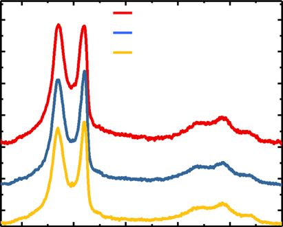
Zou et al. Light: Science & Applications (2020)9:69                                                                                                         Page 10 of 11

We thank Dr. Syed Hamad at the state key laboratory of applied optics in the            19. Guo, L. et al. Two-beam-laser interference mediated reduction, patterning and
Chinese Academy of Sciences for the revision support of this paper.                         nanostructuring of graphene oxide for the production of a flexible humidity
                                                                                            sensing device. Carbon 50, 1667–1673 (2012).
Author details                                                                          20. Birnbaum, M. Semiconductor surface damage produced by ruby lasers. J. Appl.
1                                                                                           Phys. 36, 3688–3689 (1965).
 State Key Laboratory of Applied Optics, Changchun Institute of Optics, Fine
Mechanics and Physics, Chinese Academy of Sciences, 130033 Changchun,                   21. Bonse, J. et al. Laser-induced periodic surface structures—a scientific ever-
China. 2Center of Materials Science and Optoelectronics Engineering,                        green. IEEE J. Sel. Top. Quantum Electron. 23, 9000615 (2017).
University of Chinese Academy of Sciences, 100049 Beijing, China.                       22. Öktem, B. et al. Nonlinear laser lithography for indefinitely large-area nanos-
3                                                                                           tructuring with femtosecond pulses. Nat. Photonics 7, 897–901 (2013).
 Department of Electronic Information and Physics, Changzhi University,
046011 Changzhi, China. 4Key Laboratory of Optical System Advanced                      23. Wang, L. et al. Plasmonic nano-printing: large-area nanoscale energy
Manufacturing Technology, Changchun Institute of Optics, Fine Mechanics                     deposition for efficient surface texturing. Light Sci. Appl. 6, e17112 (2017).
and Physics (CIOMP), Chinese Academy of Sciences (CAS), 130033 Changchun,               24. Huang, J. et al. Cylindrically focused nonablative femtosecond laser processing
China. 5The Institute of Optics, University of Rochester, Rochester, NY 14627,              of long-range uniform periodic surface structures with tunable diffraction
USA                                                                                         efficiency. Adv. Opt. Mater. 7, 1900706 (2019).
                                                                                        25. Huang, J. et al. Fabrication of highly homogeneous and controllable nano-
Conflict of interest                                                                         gratings on silicon via chemical etching-assisted femtosecond laser mod-
The authors declare that they have no conflict of interest.                                  ification. Nanophotonics 8, 869–878 (2019).
                                                                                        26. Sidhu, M. S., Munjal, P. & Singh, K. P. High-fidelity large area nano-patterning of
                                                                                            silicon with femtosecond light sheet. Appl. Phys. A 124, 46 (2018).
Supplementary information is available for this paper at https://doi.org/
                                                                                        27. Huang, M. et al. Origin of laser-induced near-subwavelength ripples: inter-
10.1038/s41377-020-0311-2.
                                                                                            ference between surface plasmons and incident laser. ACS Nano 3, 4062–4070
                                                                                            (2009).
Received: 16 December 2019 Revised: 1 April 2020 Accepted: 7 April 2020                 28. Shvartzburg, A., Petite, G. & Auby, N. S-polarized surface electromagnetic
                                                                                            waves in inhomogeneous media: exactly solvable models. J. Opt. Soc. Am. B
                                                                                            16, 966–970 (1999).
                                                                                        29. Kim, K. Excitation of s-polarized surface electromagnetic waves in inhomo-
                                                                                            geneous dielectric media. Opt. Express 16, 13354–13363 (2008).
References                                                                              30. Sun, Z. J. et al. Artificial TE-mode surface waves at metal surfaces mimicking
 1. Georgakilas, V. et al. Noncovalent functionalization of graphene and graphene           surface plasmons. Opt. Express 22, 4714–4722 (2014).
     oxide for energy materials, biosensing, catalytic, and biomedical applications.    31. Chitara, B. et al. Infrared photodetectors based on reduced graphene oxide
     Chem. Rev. 116, 5464–5519 (2016).                                                      and graphene nanoribbons. Adv. Mater. 23, 5419–5424 (2011).
 2. Compton, O. C. & Nguyen, S. T. Graphene oxide, highly reduced graphene              32. Cao, Y. et al. Fully suspended reduced graphene oxide photodetector with
     oxide, and graphene: versatile building blocks for carbon-based materials.             annealing temperature-dependent broad spectral binary photoresponses. ACS
     Small 6, 711–723 (2010).                                                               Photonics 4, 2797–2806 (2017).
 3. Patchkovskii, S. et al. Graphene nanostructures as tunable storage media for        33. Yao, H. B. et al. Direct fabrication of photoconductive patterns on LBL
     molecular hydrogen. Proc. Natl Acad. Sci. USA 102, 10439–10444 (2005).                 assembled graphene oxide/PDDA/titania hybrid films by photothermal and
 4. Han, N. et al. Improved heat dissipation in gallium nitride light-emitting diodes       photocatalytic reduction. J. Mater. Chem. 20, 5190–5195 (2010).
     with embedded graphene oxide pattern. Nat. Commun. 4, 1452 (2013).                 34. Flanders, D. C. Submicrometer periodicity gratings as artificial anisotropic
 5. Lin, H. et al. A 90-nm-thick graphene metamaterial for strong and extremely             dielectrics. Appl. Phys. Lett. 42, 492–494 (1983).
     broadband absorption of unpolarized light. Nat. Photonics 13, 270–276 (2019).      35. Xin, W. et al. Black-phosphorus-based orientation-induced diodes. Adv. Mater.
 6. Yan, H. G. et al. Damping pathways of mid-infrared plasmons in graphene                 30, 1704653 (2018).
     nanostructures. Nat. Photonics 7, 394–399 (2013).                                  36. Island, J. O. et al. TiS3 transistors with tailored morphology and electrical
 7. Ju, L. et al. Graphene plasmonics for tunable terahertz metamaterials. Nat.             properties. Adv. Mater. 27, 2595–2601 (2015).
     Nanotechnol. 6, 630–634 (2011).                                                    37. You, R. et al. Laser fabrication of graphene-based flexible electronics. Adv.
 8. Gomez-Diaz, J. S., Tymchenko, M. & Alù, A. Hyperbolic metasurfaces: surface             Mater. n/a, 1901981 (2019).
     plasmons, light-matter interactions, and physical implementation using gra-        38. Jiang, H. B. et al. Review of photoreduction and synchronous patterning of
     phene strips [Invited]. Optical Mater. Express 5, 2313–2329 (2015).                    graphene oxide toward advanced applications. J. Mater. Sci. 55, 480–497
 9. Liu, Z. M. et al. Three-dimensional self-organization in nanocomposite layered          (2020).
     systems by ultrafast laser pulses. ACS Nano 11, 5031–5040 (2017).                  39. Zhang, Y. L. et al. A “Yin”-“Yang” complementarity strategy for design and
10. Guo, L. J. Nanoimprint lithography: methods and material requirements. Adv.             fabrication of dual-responsive bimorph actuators. Nano Energy 68, 104302
    Mater. 19, 495–513 (2007).                                                              (2020).
11. Tokel, O. et al. In-chip microstructures and photonic devices fabricated by         40. Hummers, W. S. Jr & Offeman, R. E. Preparation of graphitic oxide. J. Am. Chem.
    nonlinear laser lithography deep inside silicon. Nat. Photonics 11, 639–645             Soc. 80, 1339 (1958).
    (2017).                                                                             41. Jiang, W. S. et al. Reduced graphene oxide-based optical sensor for detecting
12. Zheng, X. R. et al. Patterning metal contacts on monolayer MoS2 with van-               specific protein. Sens. Actuators B 249, 142–148 (2017).
    ishing Schottky barriers using thermal nanolithography. Nat. Electron. 2, 17–25     42. Gnilitskyi, I. et al. High-speed manufacturing of highly regular femtosecond
    (2019).                                                                                 laser-induced periodic surface structures: physical origin of regularity. Sci. Rep.
13. Garcia, R., Knoll, A. W. & Riedo, E. Advanced scanning probe lithography. Nat.          7, 8485 (2017).
    Nanotechnol. 9, 577–587 (2014).                                                     43. Kymakis, E. et al. Flexible organic photovoltaic cells with in situ nonthermal
14. Vorobyev, A. Y. & Guo, C. L. Direct femtosecond laser surface nano/micro-               photoreduction of spin-coated graphene oxide electrodes. Adv. Funct. Mater.
    structuring and its applications. Laser Photonics Rev. 7, 385–407 (2013).               23, 2742–2749 (2013).
15. Zhang, Y. L. et al. Direct imprinting of microcircuits on graphene oxides film by    44. Tian, H. et al. Cost-effective, transfer-free, flexible resistive random access
    femtosecond laser reduction. Nano Today 5, 15–20 (2010).                                memory using laser-scribed reduced graphene oxide patterning technology.
16. Zheng, X. R. et al. Highly efficient and ultra-broadband graphene oxide                  Nano Lett. 14, 3214–3219 (2014).
    ultrathin lenses with three-dimensional subwavelength focusing. Nat. Com-           45. Lin, J. et al. Laser-induced porous graphene films from commercial polymers.
    mun. 6, 8433 (2015).                                                                    Nat. Commun. 5, 5714 (2014).
17. Gengler, R. Y. N. et al. Revealing the ultrafast process behind the photo-          46. Gao, W. L. et al. Excitation of plasmonic waves in graphene by guided-mode
    reduction of graphene oxide. Nat. Commun. 4, 2560 (2013).                               resonances. ACS Nano 6, 7806–7813 (2012).
18. Strong, V. et al. Patterning and electronic tuning of laser scribed graphene for    47. Beltaos, A. et al. Femtosecond laser induced periodic surface structures on
    flexible all-carbon devices. ACS Nano 6, 1395–1403 (2012).                               multi-layer graphene. J. Appl. Phys. 116, 204306 (2014).
Zou et al. Light: Science & Applications (2020)9:69 Page 11 of 11
48. Kasischke, M. et al. Simultaneous nanopatterning and reduction of gra- 50. Xie, C. et al. Photodetectors based on two-dimensional layered materials
phene oxide by femtosecond laser pulses. Appl. Surf. Sci. 445, 197–203 beyond graphene. Adv. Funct. Mater. 27, 1603886 (2017).
(2018). 51. Jalil, S. A. et al. Formation of controllable 1D and 2D periodic surface structures
49. Ren, H. Y. et al. Hierarchical graphene foam for efficient omnidirectional solar- on cobalt by femtosecond double pulse laser irradiation. Appl. Phys. Lett. 115,
thermal energy conversion. Adv. Mater. 29, 1702590 (2017). 031601 (2019).You can also read