Machine Learning Chemical Guidelines for Engineering Electronic Structures in Half-Heusler Thermoelectric Materials
←
→
Page content transcription
If your browser does not render page correctly, please read the page content below
AAAS
Research
Volume 2020, Article ID 6375171, 8 pages
https://doi.org/10.34133/2020/6375171

Research Article
Machine Learning Chemical Guidelines for Engineering Electronic
Structures in Half-Heusler Thermoelectric Materials

 Maxwell T. Dylla,1 Alexander Dunn ,2,3 Shashwat Anand ,1 Anubhav Jain ,3
 and G. Jeffrey Snyder 1
 1
 Department of Materials Science and Engineering, Northwestern University, IL 60208, USA
 2
 Department of Materials Science and Engineering, UC Berkeley, CA 94720, USA
 3
 Lawrence Berkeley National Laboratory, Energy Technologies Area, CA 94720, USA

 Correspondence should be addressed to G. Jeffrey Snyder; jeff.snyder@northwestern.edu

 Received 13 January 2020; Accepted 2 March 2020; Published 22 April 2020

 Copyright © 2020 Maxwell T. Dylla et al. Exclusive Licensee Science and Technology Review Publishing House. Distributed under a
 Creative Commons Attribution License (CC BY 4.0).

 Half-Heusler materials are strong candidates for thermoelectric applications due to their high weighted mobilities and power
 factors, which is known to be correlated to valley degeneracy in the electronic band structure. However, there are over 50 known
 semiconducting half-Heusler phases, and it is not clear how the chemical composition affects the electronic structure. While all
 the n-type electronic structures have their conduction band minimum at either the Γ- or X-point, there is more diversity in the
 p-type electronic structures, and the valence band maximum can be at either the Γ-, L-, or W-point. Here, we use high
 throughput computation and machine learning to compare the valence bands of known half-Heusler compounds and discover
 new chemical guidelines for promoting the highly degenerate W-point to the valence band maximum. We do this by
 constructing an “orbital phase diagram” to cluster the variety of electronic structures expressed by these phases into groups,
 based on the atomic orbitals that contribute most to their valence bands. Then, with the aid of machine learning, we develop
 new chemical rules that predict the location of the valence band maximum in each of the phases. These rules can be used to
 engineer band structures with band convergence and high valley degeneracy.

1. Introduction [8–13]. Simple models, driven by domain knowledge, are
 especially useful for discovering ways to engineer these prop-
High thermoelectric performance requires a high thermo- erties, even when there are small amounts of available data
electric quality factor which is proportional to the weighted [14, 15]. In this work, we use machine learning to develop
mobility, μW , divided by the lattice thermal conductivity, κL simple models that explain the electronic structures of half-
[1]. High weighted mobility, which is correlated to high peak Heusler phases.
power factor, makes p-type half-Heusler materials strong To begin to understand electronic structure in the half-
candidates for thermoelectric applications. These materials Heusler family, we calculated the electronic structures’
owe their high weighted mobilities and high power factors semiconducting (18 valence electrons) phases using density
to weak electron-phonon coupling and high valley degener- functional theory (DFT). We chose stable phases reported
acy imposed by the symmetry of the Brillouin zone [2–6]. in the Inorganic Crystal Structure Database (ICSD) along-
However, there are over 50 known semiconducting half- side 10 phases predicted stable (see Methods) in previous
Heusler compounds [7], and it is not clear how the chemical studies from DFT calculations [3, 16, 17]. To quantita-
composition affects the electronic structure. In recent work, tively compare the calculated phases, we decomposed their
machine learning has become a powerful tool for engineering near band-edge electronic structures into their chemical
complex properties in cases where the known physical trends components—atomic orbitals. For domain experts, atomic
are exhausted, but there are many features left to understand orbitals are a powerful basis for interpreting electronic
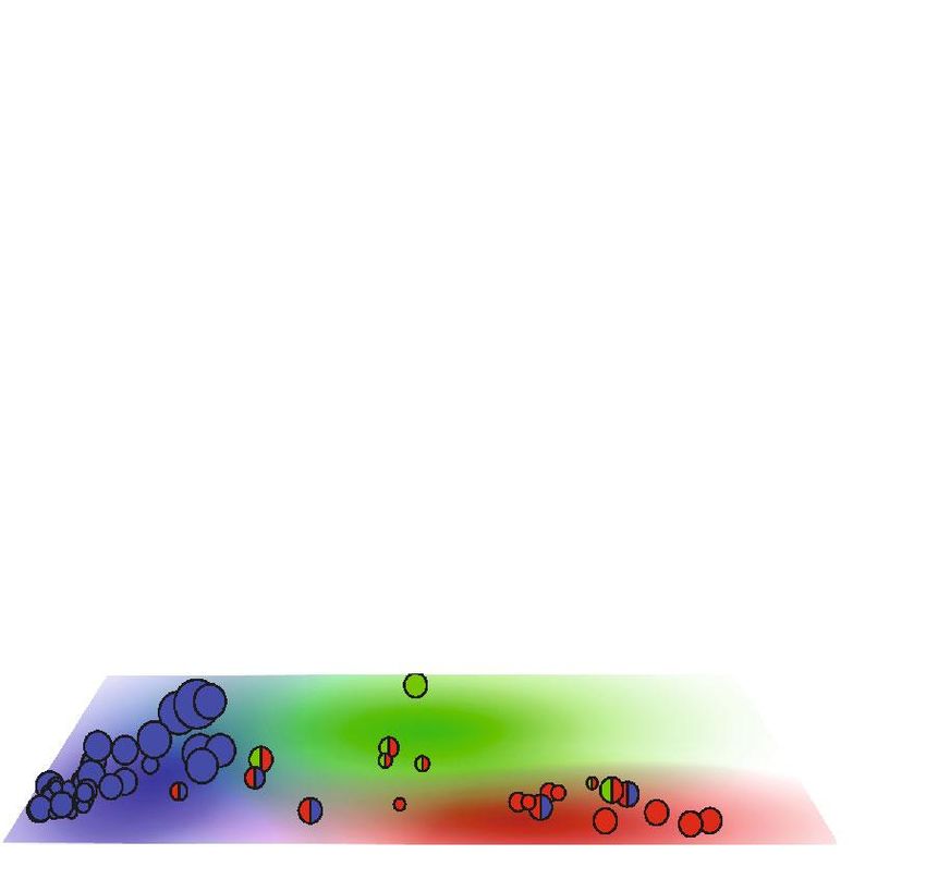
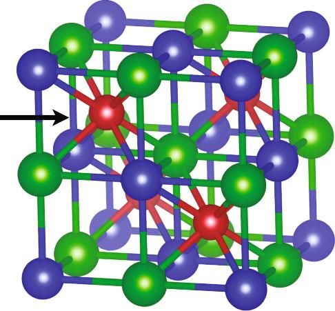
2 Research

structure [18–21]. For example, small variations in orbital
character (s/p/d) explain whether diamond-like semiconduc- X
tors have direct or indirect band gaps [22]. Based on a chem-
ical map of each phase’s atomic orbitals, we find that there Y
are three distinct classes of electronic structures in the half-
Heusler family. While all have conduction band minimum Z
at either the X-point or the Γ-point—there is more variance
in the valence bands—the valence band maximum can be at
one of three k-points in the Brillouin zone. Phases that are
intermediates of the extreme cases even have increased valley
degeneracy from the energy convergence of multiple k-points Figure 1: There are three crystallographic sites in the half-Heusler
at the valence band edge. We use machine learning to structure: X (blue), Y (red), and Z (green). The Y-site is in a
elucidate how composition affects the relative energies of these body-centered-cubic coordination environment formed by the X-
k-points, which can direct efforts to engineer band structures and Z-sites. The X- and Z-sites are in tetrahedral coordination
with high degeneracy and weighted mobility. Similar to the environments formed by the Y-sites (in the first nearest-neighbor
valence balanced rule that predicts the stability of half- shell) and octahedral coordination environments formed by X-
Heusler phases [7], we find that a new valence difference rule and Z-sites (in the second nearest-neighbor shell).
predicts the relative energies of the k-points. Instead of consid-
ering the total valence electron count (rule for stability), these
rules consider the relative valence electron configurations of
 valence states, and 97% of the variation in an orbital charac-
the elements on each site of the crystal structure (Figure 1).
 ter is accounted for by the X‐d, Y‐d, and Z‐p components
 alone (Figure S2 and Table S1). Therefore, the phases can
2. Classifying Valence-Band-Edge be represented in a Gibbs phase triangle (Figure 2(a)). In
 Electronic Structures contrast to a conventional phase diagram, which represents
 the stable phases within a composition region, the “orbital
When discussing electronic structure in crystalline materials,
 phase diagram” represents the diverse electronic structures
there are dual aspects to consider. On one hand is the recip-
 expressed by phases within a structure family.
rocal space representation—that of electronic band dia-
 There are three emergent classes of valence band electronic
grams—where electronic states are indexed by their wave
 structures (indicated by blue, red, and green). The first class of
vector, k, and band index, n. Reciprocal space holds predic-
 electronic structure (blue) has the valence band maximum at
tive information for many transport properties. For example,
 Γ, which has a degeneracy of one in the first Brillouin zone
materials with low effective mass (m∗ ) and high valley degen-
 (N vk ). To clarify, we are considering the degeneracy imposed
eracy have favorable electronic properties for thermoelectric
applications [23]. However, in this four-dimensional space, by the symmetry of the Brillouin zone, which does not include
it is difficult to study systematic changes in electronic struc- the number of degenerate bands (N vo , orbital degeneracy) at
ture with varying chemical composition. The complementary that k-point (N v = N vk · N vo ). TiNiSn is an example compound
perspective of the electronic structure is represented in real from this class, where the valence band edge is dominated by
space, where the electronic states correspond to combina- Ti-d states (Figure 2(c)). The second electronic structure class
tions of atomic orbitals [19–21]. Atomic orbitals are the com- (red) has its valence band maximum at the L-point—a degener-
ponents of electronic structures, analogous to how elements acy of four. TaFeSb exemplifies this class, where the band-edge
are the components of crystal structures. To further the anal- states are dominated by Fe-d (Figure 2(d)). In the last class of
ogy, relevant portions of the electronic structure are electronic structure (green), the valence band maximum is at
described by atomic orbital compositions. In this work, we the W-point (degeneracy of six). These electronic structures
consider the atomic orbital composition of the valence band (e.g., NbRhSn in Figure 2(b)) have relatively higher band-edge
edge using the projected density of states [24, 25]. The elec- contributions from Z‐p orbitals, which originates from the
tronic structures are computed using density functional the- states along the X‐W path (green-orange hue). Each of the
ory with the PBE functional without accounting for spin- other electronic structures are hybrids of the three classes. For
orbit coupling effects. We evaluate the fractions of states that example, NbCoSn is a hybrid between the W-point (green)
would be occupied by holes in the valence bands (see and L-point (red) extremes, with both carrier pockets within
Methods). This composition depends on the electron chem- 100 meV of the band edge. Irrespective of the electronic
ical potential (Fermi level) and temperature, but for consis- structure class, the type of atomic orbitals contributing to each
tency across multiple p-type phases, standard conditions k-point (within the first valence band) is similar among all of
were chosen. In this work, the Fermi level is placed at the the half-Heusler materials—the Γ-point is dominated by X‐d
valence band edge and the temperature is 700 K, which is states, the L-point is dominated by Y‐d states, and Z‐p states
near the temperature at the experimental peak power factor are mixed into the X‐W path. Therefore, the chemical bonding
for half-Heusler materials [3, 4]. Between the three crystallo- is similar among all the materials. The primary source of vari-
graphic sites (X/Y/Z) and three orbital characters (s/p/d), ance among their electronic structures is the relative energies
there are nine components to consider. However, only sev- of the Γ-, L-, and W-points, which are linked to the relative
eral of the components contribute meaningfully to the energies of their constituent atomic orbitals.
Research 3

 2.0
 Rh

 Z-p
 Nb Sn
 Band edge (NV)
 Effective mass 1.0
 -Converged
 ~ 1/m⁎

 0.75 NV = 6
 - (1)

 E - EF (eV)
 NbRhSn
 0.0
 -L (4)
 0.5
 -W (6)
 NbRhSn –1.0

 TiNiSn 0.25
 TaCoSn
 TaFeSb

 –2.0
 X-d Y-d X W K L U W L KIU X
 Wavevector k
 (a) (b)

 2.0 2.0
 Ni Fe

 Ti Sn Ta Sb
 1.0 1.0

 NV = 1 NV = 4
 E - EF (eV)

 E - EF (eV)

 TiNiSn TaFeSb
 0.0 0.0

 –1.0 –1.0

 –2.0 –2.0
 X W K L U W L K IU X X W K L U W L K IUX
 Wavevector k Wavevector k

 (c) (d)

Figure 2: (a) The valence band edges of half-Heusler electronic structures are primarily composed of d orbitals from the X- and Y-sites, and
secondarily, p orbitals from the Z-site. The relative contributions of these basis orbitals describe the type of carrier pockets observed in this
structure family. (b) Electronic structures with higher concentrations of Z‐p orbitals at the band edge have carrier pockets at the W-point with
high degeneracy. (c) Phases with valence band edges dominated by X‐d states have carrier pockets at the Γ-point, and (d) band edges
dominated by Y‐d states have carrier pockets at the L-point.

3. Valence Difference Rules for Engineering Γ‐L encoded in their group (column) number on the periodic
 Carrier Pockets table. In a linear model, differences in valence account for
 over 85% of the variation in the Γ‐L energy offset
Engineering the Γ‐L energy offset tunes the valley degeneracy (Figure 3). Compounds with larger differences in valence
and the thermoelectric performance of half-Heusler mate- have valence band maxima at Γ (e.g., TiNiSn, where Ni has
rials [4]. The relative energies of the Γ- and L-points are six more valence electrons than Ti), while compounds with
described by simple, chemical differences between the X- smaller differences in valence have valence band maxima at
and Y-species. The dominant, first-order effect is the differ- L (e.g., NbFeSb, where Fe has only three more valence elec-
ence in valence between the X- and Y-species, which is trons than Nb). A second-order descriptor is the difference
4 Research

 6
 Group IV and group IX
 5 (e.g., NbCoSn)

 Probability density
 4
 W
 L
 3
 L

 (a) (b) 2

 All other compounds
 1

 0.55 NbFeSb 0
 NbCoSn –2.0 –1.5 –1.0 –0.5 0.0
 EW-point - EVBM (eV)
 EL-point- E -point (eV)

 0.00
 NbRhSn Figure 4: The W-point is at or near the valence band maximum for
 TiNiSn compounds with both a group IV element on the Z-site (Sn or Ge)
 –0.55 and a group IX on the Y-site (Co, Rh, or Ir). Furthermore, in six
 of the seven W-pocket materials, the L-point is converged within
 100 meV of the band edge (total degeneracy of ten).
 L-pockets
 –1.00
 4. Engineering Highly Degenerate
 3 4 5 6 7 8 W-Pocket Materials
 Group number difference (Y-X)
 Materials that contain both group IV (e.g., Sn) and group IX
 (e.g., Co) elements adopt a distinct class of electronic struc-
 0.2 0.4 0.6 0.8 1.0 1.2
 ture, where the W-point is at or near the valence band edge
 Elec. neg. difference (Y-X)
 (Figure 4). In six of these seven phases, the W-point and
 (c) L-point are both within 100 meV of the valence band edge,
Figure 3: (a) Engineering the relative energies of the L-point and (b) effectively converged at 1200 K. The exception to the con-
the Γ-point controls the degeneracy of half-Heusler materials. (c) verged cases is NbRhSn, which is the most extreme example
The difference in valence electron configuration (encoded in group of the W-pocket class. While only Sn- and Ge-containing
number) and electronegativity of the X- and Y-species determines end-member phases are reported stable in the literature, the
the energy offset of these k-points. calculation of metastable NbCoPb confirms that this valence
 rule extends beyond Sn- and Ge-containing compounds
in Pauling’s electronegativity between the X- and Y-species, (Figure S8). Entropy-stabilized solid solutions between
which can account for differences in the Γ‐L energy offset NbCoSn and NbCoPb could benefit from reduced lattice
between compounds with isovalent species (e.g., NbCoSn thermal conductivity from alloy scattering and retain valley-
and NbRhSn). Furthermore, elemental characteristics of the high degeneracy throughout the solid solution [30–32].
Z-species do not improve the prediction of the Γ‐L energy However, the carrier density must be tuned to optimize the
offset, likely because the energies are properties of the X- thermoelectric transport properties. There are three sites
and Y-species orbitals. Recall that the Γ- and L-point states where aliovalent substitution can introduce additional holes
are formed from the X‐d and Y‐d orbitals. in the system and tune the carrier density. We have
 The valence difference rule extends beyond the semicon- computed several site-substituted end-members to
ducting phases to metastable phases with 17 and 19 valence investigate the potential changes in band structure induced
electrons [26–28], which are p- and n-type metals by candidate dopant elements (Figure S8). Substituting on
(Figure S7). For example, while the energy difference the X- and Y-sites has the expected behavior of tuning
between the Γ- and L-points is nearly zero for TiCoSb, the the Γ‐L energy offset, based on the valence difference
Γ-pocket dominates the valence band maximum in the Ni- rules developed in Section 3.
substituted analog; TiNiSb has a larger valence difference Substituting Ti on the Nb-site (X-site) raises the relative
and 19 valence electrons. Conversely, in the Fe-substituted energy of the Γ point, since the valence difference between
analog, the L-pocket dominates; TiFeSb has 17 valence Ti and Co is larger than between Nb and Co. Introducing
electrons and a smaller difference in valence. While TiNiSb Fe on the Co-site (Y-site) has the opposite effect, and pushes
and TiFeSb are not stable themselves, there are implications the L-point above the W-point, unconverging the bands.
for forming solid solutions between TiCoSb and either of However, substituting In on the Sn-site (Z-site) has an
the metallic end-members (electronic doping) [29]—the entirely new effect. In NbCoIn, the X-point is at the valence
relative energies of the Γ- and L-points may change. band edge. This compound has an entirely different class of
Research 5

electronic structure, distinct from the three archetypal band meshes. Finally, a non-self-consistent field calculation with
structures identified in Figure 2. The p states from elemental 20 × 20 × 20 gamma-centered meshes was used to calculate
In appear to promote the X-point to the valence band edge. quantitatively accurate density of states with tetrahedron
The band structure has a flat and dispersive character smearing [56]. In addition, inertial (conductivity) effective
between the X- and W-points, which is similar to the band masses were calculated using the BoltzTraP package [57].
character found in SrTiO3 and some full-Heusler phases This set of calculations were performed with the atomate
[33, 34]. There may be differences in transport properties workflow software [58]. The projected density of states and
between materials doped on each of the three sites. chemical composition were featurized in the matminer pack-
 age using the SiteDOS and ElementProperty (with pymatgen
5. Conclusions data) featurizers [59]. The Fermi surfaces of the electronic
 structures were visualized using the pymatgen package [60].
We have mapped the electronic structures of semiconducting The most important atomic features for modeling the Γ‐L
half-Heusler phases according to the atomic orbital composi- energy offset were determined by ridge regression [61]. The
tion of their valence bands. This mapping is termed an orbital calculations were performed on stable phases reported in
phase diagram, and it reveals that there are three well- the Inorganic Crystal Structure Database (ICSD) alongside
distinguished classes of electronic structures. The k-points 10 phases (HfAsIr, HfBiRh, HfNiPb, HfPdPb, NbSbOs, TaS-
forming the valence band maximum are different for each bOs, TaSnRh, TiAsIr, TiSnPd, and ZrAsIr) predicted stable
electronic structure class. The relative energies of these k in previous studies from DFT calculations [3, 16, 17].
-points can be controlled using simple rules based on the
valence electron configurations of the elemental species. 6.2. Measuring Electronic Structure Compositions. In p-type
The difference in valence between the X- and Y-species con- semiconductors, charge-transporting holes occupy states in
trols the relative energies of the Γ- and L-point energies, the valence bands according to the distribution function for
while controlling the valence of the Y- and Z-species can lead holes (h = 1 − f , where f is the Fermi-Dirac distribution
to the emergence of highly degenerate carrier pockets at the function) [62]. These valence states are ascribed to particular
W-point. These rules extend beyond the semiconducting atomic orbitals in the projected density of states (gi ). The
phases, as demonstrated by calculations of metastable 17 number of occupied holes from a particular atomic orbital
and 19 valence electron phases. (pi ) is accumulated from the valence band states (Figure S1).
 These results form a foundation for exploring the space
of possible solid solutions in this structure family. Forming ð
solid solutions is incredibly important in the half-Heusler pi = gi ðEÞ · hðEÞ · dE: ð1Þ
family for suppressing their high lattice thermal conductivi- VB

ties [4, 35–41]. While lattice thermal conductivities in solid
solutions are quantitatively described by empirical models The fractions of atomic-like holes (xi = pi /Σi pi ) describe
[30–32], changes in electronic properties are understood the composition of the system of holes in a particular
more qualitatively. To the first order, the apparent band phase. The composition depends on the Fermi level and the
structure in a solid solution is a linear interpolation between temperature. In this work, the Fermi level is placed at the
the end-member electronic structures [42–47]. For example band edge and the temperature is 700 K. When analyzing
in the Zintl structure family, the band gap and effective mass conduction bands, the Fermi-Dirac distribution function
in n-type Mg3Sb2Mg3Bi2 change linearly with composition can replace the hole distribution function.
between Mg3Sb2 and Mg3Bi2 [48]. In the III-V semiconduc-
tors, the band gap of InAs-GaAs changes linearly as well 6.3. Modeling the Γ‐L Energy Offset. Regression was used to
[49]. In future work on half-Heuslers, the effects of forming identify design principles for engineering the Γ‐L energy off-
solid solutions on the electronic structures could be studied set. Fivefold crossvalidation was used to score the trained
by calculating the backfolded band structures [50, 51] or ana- models according to the coefficient of determination (r 2 ).
lyzing their transport properties. Furthermore, the orbital The model pipeline consisted of standard scaling of the input
phase diagram technique will be useful for tracking the features (generated from the ElementProperty featurizer with
changes in electronic structure throughout the solid pymatgen data, which was applied to each crystal site) to zero
solutions. mean and unit variance, followed by ridge regression trained
 by gradient descent with early stopping. The model scoring
6. Methods was optimized over a grid of tolerance values for early
 stopping. The optimized model scores and regression
6.1. Calculation Details. Electronic structure calculations weights were collected for a series of regularization strengths
were carried out using a plane-wave basis (cutoff energy of (Figure S4/5). As the regularization penalty was decreased,
520 eV) in the VASP package with PAW pseudopotentials the X- and Y-site group number became the most
and the PBE functional [25, 52–54]. Spin-orbit coupling cor- dominant feature as measured by the regression weights.
rections were not applied to these calculations. The structural Ordinary least squares reveals that over 85% of the
degrees of freedom were relaxed using 12 × 12 × 12 variation in the energy offset is explained by the difference
Monkhorst-Pack k-point meshes [55], followed by relaxation in group number between the X- and Y-sites alone
of the electronic degrees of freedom using 15 × 15 × 15 (Figure S6).
6 Research

6.4. Modeling the W-Pocket Class. It was observed that com- [6] C. Fu, T. Zhu, Y. Pei et al., “High Band Degeneracy Contrib-
pounds with both group IV (e.g., Sn) and group IX (e.g., Co) utes to High Thermoelectric Performance in p-Type Half-
elements adopt the W-pocket type electronic structure. To Heusler Compounds,” Advanced Energy Materials, vol. 4,
confirm that this rule describes the distinct class of electronic no. 18, p. 1400600, 2014.
structure, we compared the distributions of energy offsets [7] S. Anand, K. Xia, V. I. Hegde et al., “A valence balanced rule
between compounds that follow this chemical rule and those for discovery of 18-electron half-Heuslers with defects,”
that do not (Figure 4). The distributions were estimated using Energy & Environmental Science, vol. 11, no. 6, pp. 1480–
a Gaussian kernel. It can be seen that the two distributions 1488, 2018.
are distinct. [8] L. Ward, A. Agrawal, A. Choudhary, and C. Wolverton, “A
 general-purpose machine learning framework for predicting
 properties of inorganic materials,” npj Computational Mate-
Conflicts of Interest rials, vol. 2, no. 1, 2016.
 [9] K. T. Butler, D. W. Davies, H. Cartwright, O. Isayev, and
There are no conflicts of interest to declare. A. Walsh, “Machine learning for molecular and materials sci-
 ence,” Nature, vol. 559, no. 7715, pp. 547–555, 2018.
Acknowledgments [10] A. Mansouri Tehrani, A. O. Oliynyk, M. Parry et al., “Machine
 Learning Directed Search for Ultraincompressible, Superhard
M.T.D. and G.J.S. acknowledge support from the National Materials,” Journal of the American Chemical Society,
Science Foundation (DMREF-1333335 and DMREF- vol. 140, no. 31, pp. 9844–9853, 2018.
1729487). S.A. and G.J.S. acknowledge the U.S. Department [11] J. C. Mauro, “Decoding the glass genome,” Current Opinion in
of Energy, Office of Energy Efficiency and Renewable Energy Solid State and Materials Science, vol. 22, no. 2, pp. 58–64,
(EERE) program “Accelerated Discovery of Compositionally 2018.
Complex Alloys for Direct Thermal Energy Conversion” [12] V. Stanev, C. Oses, A. G. Kusne et al., “Machine learning
(DOE award DE-AC02-76SF00515). A.D and A.J. were sup- modeling of superconducting critical temperature,” npj Com-
ported by the United States Department of Energy, Office of putational Materials, vol. 4, no. 1, 2018.
Basic Energy Sciences, Early Career Research Program [13] P. Avery, X. Wang, C. Oses et al., “Predicting superhard mate-
under award DE-AC02-05CH11231, which funds Law- rials via a machine learning informed evolutionary structure
 search,” npj Computational Materials, vol. 5, no. 1, 2019.
rence Berkeley National Laboratory. This research used
resources of the National Energy Research Scientific Com- [14] N. Wagner and J. M. Rondinelli, “Theory-Guided Machine
puting Center (NERSC), a U.S. Department of Energy Learning in Materials Science,” Frontiers in Materials, vol. 3,
 2016.
Office of Science User Facility operated under Contract
No. DE-AC02-05CH11231. [15] Y. Zhang and C. Ling, “A strategy to apply machine learning to
 small datasets in materials science,” npj Computational Mate-
 rials, vol. 4, no. 1, 2018.
Supplementary Materials [16] M. Hellenbrandt, “The Inorganic Crystal Structure Database
 (ICSD)—Present and Future,” Crystallography Reviews,
I. Measuring electronic structure compositions. II. Regres- vol. 10, no. 1, pp. 17–22, 2004.
sion of Γ‐L offset. III. Metastable compound calculations. [17] R. Gautier, X. Zhang, L. Hu et al., “Prediction and accelerated
IV. Band structures of the 18 electron half-Heuslers laboratory discovery of previously unknown 18-electron ABX
(Supplementary Materials) compounds,” Nature Chemistry, vol. 7, no. 4, pp. 308–316,
 2015.
References [18] J. K. Burdett, “From bonds to bands and molecules to solids,”
 Progress in Solid State Chemistry, vol. 15, no. 3, pp. 173–255,
 [1] K. Kamoto and T. Mori, Eds., “Thermoelectric Nanomaterials: 1984.
 Materials Design and Applications,” in Springer series in mate-
 [19] R. Hoffmann, “How Chemistry and Physics Meet in the Solid
 rials science No. Volume 182, Springer, Heidelberg; New York,
 State,” Angewandte Chemie International Edition in English,
 2013, oCLC: ocn857523120.
 vol. 26, no. 9, pp. 846–878, 1987.
 [2] J. Zhou, H. Zhu, T.-H. Liu et al., “Large thermoelectric power
 [20] W. A. Harrison, Electronic Structure and the Properties of
 factor from crystal symmetry-protected non- bonding orbital
 Solids: The Physics of the Chemical Bond, Dover Publications,
 in half-Heuslers,” Nature Communications, vol. 9, no. 1,
 Mineola, NY, USA, 1989.
 pp. 1721–1729, 2018.
 [3] H. Zhu, J. Mao, Y. Li et al., “Discovery of TaFeSb-based half- [21] P. A. Cox, The Electronic Structure and Chemistry of Solids,
 Heuslers with high thermoelectric performance,” Nature Com- Oxford University Press, Mineola, NY, USA, 2002.
 munications, vol. 10, no. 1, pp. 270–278, 2019. [22] P. Bogusławski and I. Gorczyca, “Influence of Chemistry on
 [4] H. Zhu, R. He, J. Mao et al., “Discovery of ZrCoBi based half the Energy Band Structure: AlAs Versus GaAs,” Acta Physica
 Heuslers with high thermoelectric conversion efficiency,” Polonica A, vol. 80, no. 3, pp. 433–436, 1991.
 Nature Communications, vol. 9, no. 1, pp. 2497–2499, 2018. [23] Z. M. Gibbs, F. Ricci, G. Li et al., “Effective mass and Fermi
 [5] C. Fu, T. Zhu, Y. Liu, H. Xie, and X. Zhao, “Band engineering surface complexity factor from ab initio band structure calcu-
 of high performance p-type FeNbSb based half-Heusler ther- lations,” npj Computational Materials, vol. 3, no. 1, 2017.
 moelectric materials for figure of merit zT > 1,” Energy & Envi- [24] P. E. Blochl, “Projector augmented-wave method,” Physical
 ronmental Science, vol. 8, no. 1, pp. 216–220, 2015. Review B, vol. 50, no. 24, pp. 17953–17979, 1994.
Research 7

[25] G. Kresse and J. Furthmuller, “Efficiency of ab-initio total half-Heusler phases at 800 °C,” Applied Physics Letters, vol. 88,
 energy calculations for metals and semiconductors using a no. 4, article 042106, 2006.
 plane-wave basis set,” Computational Materials Science, [41] J. Yu, C. Fu, Y. Liu et al., “Unique Role of Refractory Ta Alloy-
 vol. 6, no. 1, pp. 15–50, 1996. ing in Enhancing the Figure of Merit of NbFeSb Thermoelec-
[26] S. Anand, K. Xia, T. Zhu, C. Wolverton, and G. J. Snyder, tric Materials,” Advanced Energy Materials, vol. 8, no. 1,
 “Temperature Dependent n-Type Self Doping in Nominally p. 1701313, 2018.
 19-Electron Half-Heusler Thermoelectric Materials,” [42] I. T. Witting, T. C. Chasapis, F. Ricci et al., “The Thermoelec-
 Advanced Energy Materials, vol. 8, no. 30, p. 1801409, 2018. tric Properties of Bismuth Telluride,” Advanced Electronic
[27] K. Xia, P. Nan, S. Tan et al., “Short-range order in defective Materials, vol. 5, no. 6, p. 1800904, 2019.
 half-Heusler thermoelectric crystals,” Energy & Environmental [43] M. Wood, U. Aydemir, S. Ohno, and G. J. Snyder, “Observa-
 Science, vol. 12, no. 5, pp. 1568–1574, 2019. tion of valence band crossing: the thermoelectric properties
[28] W. G. Zeier, S. Anand, L. Huang et al., “Using the 18-Electron of CaZn2Sb2–CaMg2Sb2solid solution,” Journal of Materials
 Rule To Understand the Nominal 19-Electron Half-Heusler Chemistry A, vol. 6, no. 20, pp. 9437–9444, 2018.
 NbCoSb with Nb Vacancies,” Chemistry of Materials, vol. 29, [44] W. Li, L. Zheng, B. Ge et al., “Promoting SnTe as an Eco-
 no. 3, pp. 1210–1217, 2017. Friendly Solution for p-PbTe Thermoelectric via Band Con-
[29] S. Anand, M. Wood, Y. Xia, C. Wolverton, and G. J. Snyder, vergence and Interstitial Defects,” Advanced Materials,
 “Double Half-Heuslers,” Joule, vol. 3, no. 5, pp. 1226–1238, 2019. vol. 29, no. 17, p. 1605887, 2017.
[30] P. G. Klemens, “Thermal Resistance due to Point Defects at [45] J. Zhang, L. Song, G. K. H. Madsen et al., “Designing high-
 High Temperatures,” Physical Review, vol. 119, no. 2, performance layered thermoelectric materials through orbital
 pp. 507–509, 1960. engineering,” Nature Communications, vol. 7, no. 1, 2016.
[31] J. Yang, G. P. Meisner, and L. Chen, “Strain field fluctuation [46] J. He, X. Tan, J. Xu et al., “Valence band engineering and ther-
 effects on lattice thermal conductivity of ZrNiSn-based ther- moelectric performance optimization in SnTe by Mn-alloying
 moelectric compounds,” Applied Physics Letters, vol. 85, via a zone-melting method,” Journal of Materials Chemistry A,
 no. 7, pp. 1140–1142, 2004. vol. 3, no. 39, pp. 19974–19979, 2015.
[32] H. Wang, A. D. LaLonde, Y. Pei, and G. J. Snyder, “The Cri- [47] Y. Pei, H. Wang, and G. J. Snyder, “Band Engineering of Ther-
 teria for Beneficial Disorder in Thermoelectric Solid Solu- moelectric Materials,” Advanced Materials, vol. 24, no. 46,
 tions,” Advanced Functional Materials, vol. 23, no. 12, pp. 6125–6135, 2012.
 pp. 1586–1596, 2013. [48] K. Imasato, S. D. Kang, S. Ohno, and G. J. Snyder, “Band engi-
[33] D. I. Bilc, G. Hautier, D. Waroquiers, G.-M. Rignanese, and neering in Mg3Sb2by alloying with Mg3Bi2for enhanced ther-
 P. Ghosez, “Low-Dimensional Transport and Large Thermo- moelectric performance,” Materials Horizons, vol. 5, no. 1,
 electric Power Factors in Bulk Semiconductors by Band Engi- pp. 59–64, 2018.
 neering of Highly Directional Electronic States,” Physical [49] C. B. Geller, W. Wolf, S. Picozzi et al., “Computational band-
 Review Letters, vol. 114, no. 13, 2015. structure engineering of III–V semiconductor alloys,” Applied
[34] M. T. Dylla, S. D. Kang, and G. J. Snyder, “Effect of Two‐ Physics Letters, vol. 79, no. 3, pp. 368–370, 2001.
 Dimensional Crystal Orbitals on Fermi Surfaces and Electron [50] P. V. C. Medeiros, S. S. Tsirkin, S. Stafstrom, and J. Bjork,
 Transport in Three‐Dimensional Perovskite Oxides,” Ange- “Unfolding spinor wave functions and expectation values of
 wandte Chemie, vol. 131, no. 17, pp. 5557–5566, 2019. general operators: Introducing the unfolding-density opera-
[35] A. Tavassoli, F. Failamani, A. Grytsiv et al., “On the Half- tor,” Physical Review B, vol. 91, no. 4, 2015.
 Heusler compounds Nb1-x{Ti,Zr,Hf}xFeSb: Phase relations, [51] P. V. C. Medeiros, S. Stafström, and J. Björk, “Effects of extrin-
 thermoelectric properties at low and high temperature, and sic and intrinsic perturbations on the electronic structure of
 mechanical properties,” Acta Materialia, vol. 135, pp. 263– graphene: Retaining an effective primitive cell band structure
 276, 2017. by band unfolding,” Physical Review B, vol. 89, no. 4, 2014.
[36] C. Fu, S. Bai, Y. Liu et al., “Realizing high figure of merit in [52] G. Kresse and J. Furthmüller, “Efficient iterative schemes
 heavy-band p -type half-Heusler thermoelectric materials,” forab initiototal-energy calculations using a plane-wave
 Nature Communications, vol. 6, no. 1, 2015. basis set,” Physical Review B, vol. 54, no. 16, pp. 11169–
[37] E. Rausch, B. Balke, S. Ouardi, and C. Felser, “Enhanced ther- 11186, 1996.
 moelectric performance in the p-type half-Heusler (Ti/Zr/Hf [53] J. P. Perdew, K. Burke, and M. Ernzerhof, “Generalized Gradi-
 )CoSb0.8Sn0.2system via phase separation,” Physical Chemis- ent Approximation Made Simple,” Physical Review Letters,
 try Chemical Physics, vol. 16, no. 46, pp. 25258–25262, 2014. vol. 77, no. 18, pp. 3865–3868, 1996.
[38] R. He, H. S. Kim, Y. Lan, D. Wang, S. Chen, and Z. Ren, [54] G. Kresse and D. Joubert, “From ultrasoft pseudopotentials to
 “Investigating the thermoelectric properties of p-type half- the projector augmented-wave method,” Physical Review B,
 Heusler Hfx(ZrTi)1−xCoSb0.8Sn0.2by reducing Hf concen- vol. 59, no. 3, pp. 1758–1775, 1999.
 tration for power generation,” RSC Advances, vol. 4, no. 110, [55] H. J. Monkhorst and J. D. Pack, “Special points for Brillouin-
 pp. 64711–64716, 2014. zone integrations,” Physical Review B, vol. 13, no. 12,
[39] S. R. Culp, J. W. Simonson, S. J. Poon, V. Ponnambalam, pp. 5188–5192, 1976.
 J. Edwards, and T. M. Tritt, “(Zr,Hf)Co(Sb,Sn) half-Heusler [56] P. E. Blöchl, O. Jepsen, and O. K. Andersen, “Improved tetra-
 phases as high-temperature (>700°C) p-type thermoelectric hedron method for Brillouin-zone integrations,” Physical
 materials,” Applied Physics Letters, vol. 93, no. 2, article Review B, vol. 49, no. 23, pp. 16223–16233, 1994.
 022105, 2008. [57] G. K. Madsen and D. J. Singh, “BoltzTraP. A code for calculat-
[40] S. R. Culp, S. J. Poon, N. Hickman, T. M. Tritt, and J. Blumm, ing band-structure dependent quantities,” Computer Physics
 “Effect of substitutions on the thermoelectric figure of merit of Communications, vol. 175, no. 1, pp. 67–71, 2006.
8 Research

[58] K. Mathew, J. H. Montoya, A. Faghaninia et al., “Atomate: A
 high-level interface to generate, execute, and analyze computa-
 tional materials science workflows,” Computational Materials
 Science, vol. 139, pp. 140–152, 2017.
[59] L. Ward, A. Dunn, A. Faghaninia et al., “Matminer: An open
 source toolkit for materials data mining,” Computational
 Materials Science, vol. 152, pp. 60–69, 2018.
[60] S. P. Ong, W. D. Richards, A. Jain et al., “Python Materials
 Genomics (pymatgen): A robust, open-source python library
 for materials analysis,” Computational Materials Science,
 vol. 68, pp. 314–319, 2013.
[61] F. Pedregosa, G. Varoquaux, A. Gramfort et al., Machine learn-
 ing in Python, 6.
[62] N. W. Ashcroft and N. D. Mermin, Solid State Physics, Holt,
 Rinehart and Winston, New York, NY, USA, 1976.
You can also read


