Neural Cache: Bit-Serial In-Cache Acceleration of Deep Neural Networks

Page created by Jamie Knight
 
CONTINUE READING
Neural Cache: Bit-Serial In-Cache Acceleration of Deep Neural Networks
To appear in the 45th ACM/IEEE International Symposium on Computer Architecture (ISCA 2018)

                                                 Neural Cache: Bit-Serial In-Cache Acceleration of Deep Neural Networks

                                                            Charles Eckert, Xiaowei Wang, Jingcheng Wang, Arun Subramaniyan,
                                                              Ravi Iyer† , Dennis Sylvester, David Blaauw, and Reetuparna Das
                                                                       University of Michigan       † Intel Corporation

                                            {eckertch, xiaoweiw, jiwang, arunsub, dmcs, blaauw, reetudas}@umich.edu, ravishankar.iyer@intel.com
arXiv:1805.03718v1 [cs.AR] 9 May 2018

                                           Abstract—This paper presents the Neural Cache architecture,       In this paper, we instead completely eliminate the line
                                        which re-purposes cache structures to transform them into         that distinguishes memory from compute units. Similar
                                        massively parallel compute units capable of running inferences    to the human brain, which does not separate these two
                                        for Deep Neural Networks. Techniques to do in-situ arithmetic
                                        in SRAM arrays, create efficient data mapping and reducing        functionalities distinctly, we perform computation directly
                                        data movement are proposed. The Neural Cache architecture         on the bit lines of the memory itself, keeping data in-place.
                                        is capable of fully executing convolutional, fully connected,     This eliminates data movement and hence significantly
                                        and pooling layers in-cache. The proposed architecture also       improves energy efficiency and performance. Furthermore,
                                        supports quantization in-cache.                                   we take advantage of the fact that over 70% of silicon
                                           Our experimental results show that the proposed architec-
                                        ture can improve inference latency by 18.3× over state-of-art     in today’s processor dies simply stores and provides data
                                        multi-core CPU (Xeon E5), 7.7× over server class GPU (Titan       retrieval; harnessing this area by re-purposing it to perform
                                        Xp), for Inception v3 model. Neural Cache improves inference      computation can lead to massively parallel processing.
                                        throughput by 12.4× over CPU (2.2× over GPU), while reduc-           The proposed approach builds on an earlier silicon test
                                        ing power consumption by 50% over CPU (53% over GPU).             chip implementation [8] and architectural prototype [9] that
                                          Keywords-Cache, In-memory architecture,         Convolution     shows how simple logic operations (AND/NOR) can be
                                        Neural Network, Bit-serial architecture                           performed directly on the bit lines in a standard SRAM array.
                                                                                                          This is performed by enabling SRAM rows simultaneously
                                                             I. I NTRODUCTION                             while leaving the operands in-place in memory. This paper
                                                                                                          presents the Neural Cache architecture which leverages these
                                           In the last two decades, the number of processor cores         simple logic operations to perform arithmetic computation
                                        per chip has steadily increased while memory latency has          (add, multiply, and reduction) directly in the SRAM array by
                                        remained relatively constant. This has lead to the so-called      storing the data in transposed form and performing bit-serial
                                        memory wall [1] where memory bandwidth and memory                 computation while incurring only an estimated 7.5% area
                                        energy have come to dominate computation bandwidth                overhead (translates to less than 2% area overhead for the
                                        and energy. With the advent of data-intensive system, this        processor die). Each column in an array performs a separate
                                        problem is further exacerbated and as a result, today a large     calculation and the thousands of memory arrays in the cache
                                        fraction of energy is spent in moving data back-and-forth         can operate concurrently.
                                        between memory and compute units. At the same time, neural           The end result is that cache arrays morph into massive
                                        computing and other data intensive computing applications         vector compute units (up to 1,146,880 bit-serial ALU slots
                                        have emerged as increasingly popular applications domains,        in a Xeon E5 cache) that are one to two orders of magnitude
                                        exposing much higher levels of data parallelism. In this paper,   larger than modern graphics processor’s (GPU’s) aggregate
                                        we exploit both these synergistic trends by opportunistically     vector width. By avoiding data movement in and out of
                                        leveraging the huge caches present in modern processors to        memory arrays, we naturally save vast amounts of energy
                                        perform massively parallel processing for neural computing.       that is typically spent in shuffling data between compute
                                           Traditionally, researchers have attempted to address           units and on-chip memory units in modern processors.
                                        the memory wall by building a deep memory hierarchy.                 Neural Cache leverages opportunistic in-cache computing
                                        Another solution is to move compute closer to memory,             resources for accelerating Deep Neural Networks (DNNs).
                                        which is often referred to as processing-in-memory (PIM).         There are two key challenges to harness a cache’s computing
                                        Past PIM [2]–[4] solutions tried to move computing logic          resources. First, all the operands participating in an in-situ
                                        near DRAM by integrating DRAM with a logic die                    operation must share bit-lines and be mapped to the same
                                        using 3D stacking [5]–[7]. This helps reduce latency and          memory array. Second, intrinsic data parallel operations
                                        increase bandwidth, however, the functionality and design of      in DNNs have to be exposed to the underlying parallel
                                        DRAM itself remains unchanged. Also, this approach adds           hardware and cache geometry. We propose a data layout
                                        substantial cost to the overall system as each DRAM die           and execution model that solves these challenges, and
                                        needs to be augmented with a separate logic die. Integrating      harnesses the full potential of in-cache compute capabilities.
                                        computation on the DRAM die itself is difficult since the         Further, we find that thousands of in-cache compute units
                                        DRAM process is not optimized for logic computation.              can be utilized by replicating data and improving data reuse.
Neural Cache: Bit-Serial In-Cache Acceleration of Deep Neural Networks
Many Filters
Techniques for low-cost replication, reducing data movement                            (M)
overhead, and improving data reuse are discussed.                               C
                                                                                                                              Output
                                                                                                   Input Image                Image
  In summary, this paper offers the following contributions:                                  C
                                                                               R
• This is the first work to demonstrate in-situ arithmetic com-                     1
  pute capabilities for caches. We present a compute SRAM                               S
                                                                                             H                     E
  array design which is capable of performing additions and
                                                                                C                                                       M
  multiplications. A critical challenge for enabling complex                                                                  F
  operations in cache is facilitating interaction between bit                                       W
                                                                               R
  lines. We propose a novel bit-serial implementation with                          M
  transposed data layout to address the above challenge. We                             S
  designed an 8T SRAM-based hardware transpose unit for                Figure 1: Computation of a convolution layer.
  dynamically transposing data on the fly.
• Compute capabilities transform caches to massively                                                                                                BLn
                                                                                                          BLB0          BL0             BLBn
  data-parallel co-processors at negligible area cost. For
  example, we can re-purpose the 35 MB Last Level Cache
  (LLC) in the server class Intel Xeon E5 processor to                                                WLi        0 1                          0 1

  support 1,146,880 bit-serial ALU slots. Furthermore,
  in-situ computation in caches naturally saves the on-chip                                           WLj        1 0                          0 1
  data movement overheads.                                                                                       Vref
• We present the Neural Cache architecture which re-
                                                                                                            SA      SA                   SA      SA
  purposes last-level cache to accelerate DNN inferences.
  A key challenge is exposing the parallelism in DNN
  computation to the underlying cache geometry. We propose                                              WLi NOR WLj                           WLi AND WLj
  a data layout that solves these challenges, and harnesses                    (a)                                                (b)
  the full potential of in-cache compute capabilities. Further,   Figure 2: (a) Prototype test chip [8] (b) SRAM circuit
  techniques which reduce data movement overheads are             for in-place operations. Two rows (WLi and WLj )
  discussed.                                                      are simultaneously activated. An AND operation is
• The Neural Cache architecture is capable of fully executing     performed by sensing bit-line (BL). A NOR operation
  convolutional, fully connected, and pooling layers in-cache.    is performed by sensing bit-line complement (BLB).
  The proposed architecture also supports quantization and        the corresponding filter pixel and repeated across the M
  normalization in-cache. Our experimental results show that      dimension. The results across the R×S, i.e. the height and
  the proposed architecture can improve inference latency         width, are accumulated together. Further, the channels are
  by 18.3× over state-of-the-art multi-core CPU (Xeon E5),        also reduced into a single element. Thus each window gives
  7.7× over server class GPU (Titan Xp), for the Inception        us an output of 1×1×M . The window is slid using a stride
  v3 model. Neural Cache improves inference throughput            (U), increasing the stride will decrease the number of output
  by 12.4× over CPU (2.2× over GPU), while reducing               elements computed. Eventually the sliding window will
  power consumption by 59% over CPU (61% over GPU).               produce an output image with dimensions based on the height
                                                                  and width of the input, and the stride. The output’s channel
                     II. BACKGROUND                               size is equivalent to the M dimension of the filter. The
A. Deep Neural Networks                                           output image, after an activation function that varries across
   Deep Neural Networks (DNN) have emerged as popular             networks and layers, is fed as the input to the next layer.
machine learning tools. Of particular fame are Convolutional         The convolutions performed can be broken down to many
Neural Networks (CNN) which have been used for various vi-        different dimensions of matrix-vector multiplications. Neural
sual recognition tasks ranging from object recognition and de-    Cache breaks down a convolution to vector-vector dot product
tection to scene understanding. While Neural Cache can accel-     (vector dimension R × S), followed by reduction across
erate the broader class of DNNs, this paper focuses on CNNs.      channels (C). The different filter batches (M) are computed
   CNNs consist of multiple convolution layers with               in parallel using the above step. A new input vector is used
additional pooling, normalization, and fully connected layers     for each stride. In this paper we analyze the state-of-art
mixed in. Since convolutional layers are known to account         Inception v3 model which has 94 convolutional sub-layers.
for over 90% of inference operations [10], [11], we discuss       Neural Cache is utilized to accelerate not only convolutional
them in this section. A convolutional layer performs a            layers, but also pooling and fully connected layers.
convolution on the filter and the input image. Filters have
four dimensions, a height (R), width (S), channels (C), and       B. Bit-Line Computing
batches of 3D filters (M). Inputs have three dimensions with a       Neural Cache builds on earlier work on SRAM bit
height (H), width (W), and channel (C). The filter is overlaid    line circuit technology [8], [12], [13] shown in Figure 2b.
on the inputs and each pixel of the input is multiplied by        To compute in-place, two word-lines are activated
Neural Cache: Bit-Serial In-Cache Acceleration of Deep Neural Networks
simultaneously. Computation (and and nor) on the data              interaction between bit lines. Consider supporting an addition
stored in the activated word-lines is performed in the analog      operation which requires carry propagation between bit lines.
domain by sensing the shared bit-lines. Compute cache [9]          We propose bit-serial implementation with transposed
uses this basic circuit framework along with extensions to         data layout to address the above challenge.
support additional operations: copy, bulk zeroing, xor,
equality comparison, and search.                                   A. Bit-Serial Arithmetic
   Data corruption due to multi-row access is prevented by            Bit-serial computing architectures have been widely used
lowering the word-line voltage to bias against the write of the    for digital signal processing [16], [17] because of their ability
SRAM array. Measurements across 20 fabricated 28 nm test           to provide massive bit-level parallelism at low area costs. The
chips (Figure 2a) demonstrate that data corruption does not        key idea is to process one bit of multiple data elements every
occur even when 64 word-lines are simultaneously activated         cycle. This model is particularly useful in scenarios where
during such an in-place computation. Compute cache however         the same operation is applied to the same bit of multiple data
only needs two. Monte Carlo simulations also show a stability      elements. Consider the following example to compute the
of more than six sigma robustness, which is considered indus-      element-wise sum of two arrays with 512 32-bit elements. A
try standard for robustness against process variations. The ro-    conventional processor would process these arrays element-
bustness comes at the the cost of increase in delay during com-    by-element taking 512 steps to complete the operation. A bit-
pute operations. But, they have no effect on conventional array    serial processor, on the other hand, would complete the opera-
read/write accesses. The increased delay is more than com-         tion in 32 steps as it processes the arrays bit-slice by bit-slice
pensated by massive parallelism exploited by Neural Cache.         instead of element-by-element. Note that a bit-slice is com-
C. Cache Geometry                                                  posed of bits from the same bit position, but corresponding to
                                                                   different elements of the array. Since the number of elements
   We provide a brief overview of a cache’s geometry in a
                                                                   in arrays is typically much greater than the bit-precision for
modern processor. Figure 3 illustrates a multi-core processor
                                                                   each element stored in them, bit-serial computing architec-
modeled loosely after Intel’s Xeon processors [14], [15].
                                                                   tures can provide much higher throughput than bit-parallel
Shared Last Level Cache (LLC) is distributed into many slices
                                                                   arithmetic. Note also that bit-serial operation allows for flex-
(14 for Xeon E5 we modeled), which are accessible to the
                                                                   ible operand bit-width, which can be advantageous in DNNs
cores through a shared ring interconnect (not shown in figure).
                                                                   where the required bit width can vary from layer to layer.
Figure 3 (b) shows a slice of LLC cache. The slice has 80
                                                                      Note that although bit-serial computation is expected to
32KB banks organized into 20 ways. Each bank is connected
                                                                   have higher latency per operation, it is expected to have
by two 16KB sub-arrays. Figure 3 (c) shows the internal or-
                                                                   significantly larger throughput, which compensates for higher
ganization of one 16KB sub-array, composed of 8KB SRAM
                                                                   operation latency. For example, the 8KB SRAM array is com-
arrays. Figure 3 (d) shows one 8KB SRAM array. A SRAM
                                                                   posed of 256 word lines and 256 bit lines and can operate at
array is organized into multiple rows of data-storing bit-
                                                                   a maximum frequency of 4 GHz for accessing data [14], [15].
cells. Bit-cells in the same row share one word line, whereas
                                                                   Up to 256 elements can be processed in parallel in a single
bit-cells in the same column share one pair of bit lines.
                                                                   array. A 2.5 MB LLC slice has 320 8KB arrays as shown
   Our proposal is to perform in-situ vector arithmetic
                                                                   in Figure 3. Haswell server processor’s 35 MB LLC can
operations within the SRAM arrays (Figure 3 (d)). The
                                                                   accommodate 4480 such 8KB arrays. Thus up to 1,146,880
resulting architecture can have massive parallelism by
                                                                   elements can be processed in parallel, while operating at
repurposing thousands of SRAM arrays (4480 arrays in
                                                                   frequency of 2.5 GHz when computing. By repurposing mem-
Xeon E5) into vector computational units.
                                                                   ory arrays, we gain the above throughput for near-zero cost.
   We observe that LLC access latency is dominated by
                                                                   Our circuit analysis estimates an area overhead of additional
wire delays inside a cache slice, accessing upper-level cache
                                                                   bit line peripheral logic to be 7.5% for each 8KB array. This
control structures, and network-on-chip. Thus, while a typical
                                                                   translates to less than 2% area overhead for the processor die.
LLC access can take ∼30 cycles, an SRAM array access
is only 1 cycle (at 4 GHz clock [14]). Fortunately, in-situ
                                                                   B. Addition
architectures such as Neural Cache require only SRAM array
accesses and do not incur the overheads of a traditional cache        In conventional architectures, arrays are generated, stored,
access. Thus, vast amounts of energy and time spent on             accessed, and processed element-by-element in the vertical
wires and higher-levels of memory hierarchy can be saved.          direction along the bit lines. We refer to this data layout as
                                                                   the bit-parallel or regular data layout. Bit-serial computing
            III. N EURAL C ACHE A RITHMETIC                        in SRAM arrays can be realized by storing data elements
   Compute cache [9] supported several simple operations           in a transpose data layout. Transposing ensures that all bits
(logical and copy). These operations are bit-parallel              of a data element are mapped to the same bit line, thereby
and do not require interaction between bit lines. Neural           obviating the necessity for communication between bit
Cache requires support for more complex operations                 lines. Section III-F discusses techniques to store data in a
(addition, multiplication, reduction). The critical challenge in   transpose layout. Figure 4 shows an example 12×4 SRAM
supporting these complex computing primitives is facilitating      array with transpose layout. The array stores two vectors
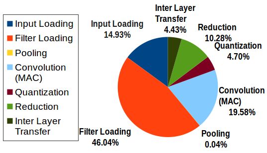
Neural Cache: Bit-Serial In-Cache Acceleration of Deep Neural Networks
8kB SRAM array
                                                                                                                                                      BL/BLB
                                                                                                                                                                                           255
                                                                                                                                             0                                              WL
                                                                                            Chunk 63

                                                                                                                  2:1
                                                                                            Chunk 62
                                                                                                                                             A
                                                                                                                                             B

                                                                                                   I/O
                                                                                     SRAM                  SRAM

                                                                                                     4:1
                                                                                             4:1
                                                                                                                            Row
                                       TMU                                                                                decoders

                                                                                                                  2:1
                                                     CBOX
                                                                                             Decoder                                       255

                                                                                                                  2:1
                                                                                                                                         Logic                       = A op B
                                                                                                                                           BL                 BLB

                                                                                                   I/O
                                                                                     SRAM                  SRAM

                                                                                                     4:1
                                                                                             4:1
                                                                                                                                                                             Vref

                                                                                                                                                              SA
                                                                                                                                            SA
                                                                                             Chunk 1                                          A&B                  ~A & ~B

                                                                                                                  2:1
                                                         LS
                                                                                             Chunk 0
                             Way 1
                                     Way 2

                                                                                                                                                                     DR
                                                                           Way 20
                                                                                                                                                        A^B
                                                                  Way 19
                                                                                                                                                              S
                                                                                                                                                Cout
                        32kB                 16kB subarray              Tag,                                                                              S = A^B^C
                                                                       State,                                                                                                C_EN

                                                                                                                                                   EN
                        data

                                                                                                                                             D
                                                                                                                                              CQ
                                             16kB subarray              LRU                                                                     Cin
                        bank

Figure 3: Neural Cache overview. (a) Multi-core processor with 8-24 LLC slices. (b) Cache geometry of a single
2.5MB LLC cache slice with 80 32KB banks. Each 32KB bank has two 16KB sub-arrays. (c) One 16KB sub-array
composed of two 8KB SRAM arrays. (d) One 8KB SRAM array re-purposed to store data and do bit line
computation on operand stored in rows (A and B). (e) Peripherals of the SRAM array to support computation.
           Word 2

                             Word 2

                                                     Word 2

                                                                           Word 2

                                                                                             Word 2
           Word 1
           Word 3
           Word 4

                             Word 1
                             Word 3
                             Word 4

                                                     Word 1
                                                     Word 3
                                                     Word 4

                                                                           Word 1
                                                                           Word 3
                                                                           Word 4

                                                                                             Word 1
                                                                                             Word 3
                                                                                             Word 4

                                                                                                                        C 1 C 2 C 3C 4   C 1 C 2 C 3C 4   C 1,3 C 2,4        C 1,3 C 2,4    C 1,2,3,4

Vector A   0                  0                      0                     0          RWL     0
           1                  1                      1         RWL         1                  1
           1                  1              RWL     1                     1                  1
           0         RWL      0                      0                     0                  0
Vector B   0                  0                      0                     0          RWL     0
           0                  0                      0          RWL        0                  0
           1                  1               RWL    1                     1                  1
           1          RWL     1                      1                     1                  1
    Sum    1                  1                      1                     1          WWL     1
                                                               WWL         0                  0
                                             WWL     0                     0                  0
                     WWL      1                      1                     1                  1
   Carry   0 0 0 0   Carry   0 0 0 0         Carry   1 0 0 0   Carry       1 0 0 0   Carry    0 0 0 0

                                  Figure 4: Addition operation                                                               Figure 5: Reduction Operation

A and B, each with four 4-bit elements. Four word lines                               simultaneously sense and wire-and the value in cells on the
are necessary to store all bit-slices of 4-bit elements.                              same bit line. To prevent the value in the bit cell from being
                                                                                      disturbed by the sensing phase, the RWL voltage should be
   We use the addition of two vectors of 4-bit numbers to                             lower than the normal VDD. The sense amps and logic gates
explain how addition works in the SRAM. The 2 words                                   in the column peripheral (Section III-E) use the 2 bit cells
that are going to be added together have to be put in the                             as operands and carry latch as carry-in to generate sum and
same bit line. The vectors A and B should be aligned in the                           carry-out. In the second half of the cycle, a write word line
array like Figure 4. Vector A occupies the first 4 rows of                            (WWL) is activated to store back the sum bit. The carry-out
the SRAM array and vector B the next 4 rows. Another 4                                bit overwrites the data in the carry latch and becomes the
empty rows of storage are reserved for the results. There                             carry-in of the next cycle. As demonstrated in Figure 4, in
is a row of latches inside the column peripheral for the                              cycles 2, 3, and 4, we repeat the first cycle to add the second,
carry storage. The addition algorithm is carried out bit-by-bit                       third, and fourth bit respectively. Addition takes n + 1, to
starting from the least significant bit (LSB) of the two words.                       complete with the additional cycle to write a carry at the end.
There are two phases in a single operation cycle. In the first
half of the cycle, two read word lines (RWL) are activated to
0          1 0      1   RWL       0     1 0       1                0        1 0           1                    0   1 0     1
                                                                                                      Product     0                                 0                                0                                           0
                                                                                                                             0    0   0                   0     0   0                         0       0     0                        0   0   0
                                                                                                                  0          0    0   0             0     0     0   0                0        0       0     0                    0   0   0   0
                                                                                                                  0          0    0   0             0     0     0   0                0        0       0     0        WWL         0   1   0   1
                                                                                                                  0          0    0   0             0     0     0   0    WWL         0        0       0     1                    0   0   0   1
                                                                                                         Carry    0 0 0 0                 Carry     0 0 0 0              Carry       0 0 0 0                     Carry           0 0 0 0
                                                                                                          Tag     0 0 0 0                  Tag      0 1 0 1               Tag        0 1 0 1                      Tag            0 1 0 1
                                                                                                                      Initial                       Cycle 1:                         Cycle 2:                                    Cycle 3:
                                                                                                                                                    Load T                            Copy                                        Copy

                                                                                                                                                                                                                                 Word 2
                                                                                                                                                                                                                                 Word 1
                                                                                                                                                                                                                                 Word 3
                                                                                                                                                                                                                                 Word 4
            Word 2

                                      Word 2

                                                              Word 2

                                                                                      Word 2
            Word 1
            Word 3
            Word 4

                                      Word 1
                                      Word 3
                                      Word 4

                                                              Word 1
                                                              Word 3
                                                              Word 4

                                                                                      Word 1
                                                                                      Word 3
                                                                                      Word 4

                                                                                                                                                    Word 2
                                                                                                                  Word 2

                                                                                                                                                                                     Word 2
                                                                                                                                                    Word 1
                                                                                                                                                    Word 3
                                                                                                                                                    Word 4
                                                                                                                  Word 1
                                                                                                                  Word 3
                                                                                                                  Word 4

                                                                                                                                                                                     Word 1
                                                                                                                                                                                     Word 3
                                                                                                                                                                                     Word 4
Vector A

            0    1 1      1           0   1 1     1           0   1 1     1   RWL     0   1 1     1               0           1   1   1               0   1     1   1        RWL         0        1    1    1                    0   1   1   1
            1    0 1      1           1   0 1     1   RWL     1   0 1     1           1   0 1     1               1           0   1   1   RWL         1   0     1   1                    1        0    1    1                    1   0   1   1
Vector B

            0    0 1      1           0   0 1     1           0   0 1     1           0   0 1     1       RWL     0           0   1   1               0   0     1   1                    0        0    1    1                    0   0   1   1
            0    1 0      1   RWL     0   1 0     1           0   1 0     1           0   1 0     1               0           1   0   1               0   1     0   1                    0        1    0    1                    0   1   0   1
Product     0    0    0   0           0   0   0   0           0   0   0   0           0   0   0   0               0           0   0   0               0   0     0   0                    0        0    0    0        WWL         0   0   0   1
            0    0    0   0           0   0   0   0           0   0   0   0           0   0   0   0               0           0   0   0               0   0     0   0        WWL         0        0    1    0                    0   0   1   0
            0    0    0   0           0   0   0   0           0   0   0   0   WWL     0   1   0   1               0           1   0   1   WWL         0   1     1   0                    0        1    1    0                    0   1   1   0
            0    0    0   0           0   0   0   0   WWL     0   0   0   1           0   0   0   1               0           0   0   1               0   0     0   1                    0        0    0    1                    0   0   0   1

    Carry   0 0 0 0           Carry   0 0 0 0         Carry   0 0 0 0         Carry   0 0 0 0             Carry   0 0 0 0                 Carry     0 0 0 1                  Carry       0 0 0 1                     Carry       0 0 0 1
     Tag    0 0 0 0            Tag    0 1 0 1          Tag    0 1 0 1          Tag    0 1 0 1              Tag    0 0 1 1                  Tag      0 0 1 1                   Tag        0 0 1 1                     Tag         0 0 1 1
                Initial               Cycle 1:                Cycle 2:                Cycle 3:                    Cycle 4:                            Cycle 5:                           Cycle 6:                                Cycle 7:
                                      Load T                   Copy                    Copy                       Load T                               Copy                               Copy                                   Store C
                     Figure 6: Multiplication Operation, each step is shown with four different sets of operands

                                                                                      Word 2
                                                                                      Word 1
                                                                                      Word 3
                                                                                      Word 4
                                      Word 2
            Word 2

                                                              Word 2
                                      Word 1
                                      Word 3
                                      Word 4
            Word 1
            Word 3
            Word 4

                                                              Word 1
                                                              Word 3
                                                              Word 4

C. Multiplication                                                                                           When the elements to be reduced do not fit in the same
                                                                                                        SRAM array, reductions must be performed across arrays
                                      bit-serial RWL
             0    1   1   1           0   1   1   1    0 1 1 1                        0   1   1   1
   We demonstrate
            1 0 1 1 RWL
                        how 1 0 1 1               multiplication
                                                  1 0 1 1
                                                               is achieved
                                                                    1 0 1 1
                                                                                                        which can be accomplished by inter-array moves. In DNNs,
based on addition and predication using the example of a 2-                                             reduction is typically performed across channels. In the
bit multiplication.    In addition    to the carry     latch, an extra   row                            model we examined, our optimized data mapping is able to
     RWL 0 0 1 1              0 0 1 1             0 0 1 1           0 0 1 1
of storage,0 the1 0tag
                     1 latch, 0is 1added
                                     0 1   to bottom
                                                  0 1 0of1 the array.
                                                                    0 1 The0 1
                                                                                                        fit all channels in the space of two arrays which sharing sense
tag bit is used
            0 0 0as0 an enable0 0 signal
                                     0 0   to the 0bit0 line  WWL 0 When
                                                         0 0 driver.    0 0 1
            0 0 0 0           0 0 0 0     WWL will0 0 1 0           0 0 1 0                             amps. We employ a technique called packing that allows us to
the tag is one,    the addition
            0 1 0 1 WWL 0 1 1 0
                                   result sum           be written back
                                                  0 1 1 0           0 1 1 to0
                                                                                                        reduce the number of channels in large layers (Section IV-A).
the array. If0 the
                0 0 tag
                     1   is zero,
                              0 0 the0 1 data in the
                                                  0 0 array
                                                         0 1   will remain.
                                                                    0 0 0 1

TwoCarry    0 0 of
      vectors          Carrynumbers,
                  0 02-bit    0 0 0 1 A   Carry
                                             and 0B,0 are     Carry 0 in0 the
                                                         0 1 stored       0 1
      Tag 0 0 1 1 Tag 0 0 1 1               Tag 0 0 1 1 Tag 0 0 1 1                                                                                                             BL                          BLB
transposedCycle
              fashion         Cycle 5:as shownCycle
                    4: and aligned                         6:
                                                   in Figure        Cycle 7:
                                                                6. Another
                                                                     Store C                                                                Column	
  Peripheral
4 empty rows      are reservedCopy
              Load T
                                    for the product Copy
                                                         and initialized to
zero. Suppose A is a vector of multiplicands and B is a vector
of multipliers. First, we load the LSB of the multiplier to the
tag latch. If the tag equals one, the multiplicand in that bit                                                                                                                                                                   Vref

                                                                                                                                                                                                                SA
                                                                                                                                                                                   SA
line will be copied to product in the next two cycles, as if it
                                                                                                                                                              DR

                                                                                                                                      WPS                                DR
                                                                                                                                                                        En
                                                                                                                                                          En

is added to the partial product. Next, we load the second bit                                                                                                                        A&B                         ~A	
  &	
  ~B
of the multiplier to the tag. If tag equals 1, the multiplicand
in that bit line will be added to the second and third bit of                                                                Predication                                                              A^B
                                                                                                                                                              MUX
                                                                                                                                                              4:1

the product in the next two cycles, as if a shifted version
of A is added to the partial product. Finally, the data in the                                                                                      Tag
                                                                                                                                                                                                            S
carry latch is stored to the most significant bit of the product.                                                                                                                    Cout
                                                                                                                                                  Q
                                                                                                                                              TEN
                                                                                                                                                  D

Including the initialization steps, it takes n2 +5n−2 cycles                                                                      T_EN                                                                                           C_EN
                                                                                                                                                                                             EN
                                                                                                                                                                                     D
                                                                                                                                                                                     CQ

to finish an n-bit multiplication. Division can be supported                                                                                                                         Cin
using a similar algorithm and takes 1.5n2 +5.5n cycles.
                                                                                                                                                          DIN                DOUT
D. Reduction                                                                                                          	
          Figure 7: Bit line peripheral design
   Reduction is a common operation for DNNs. Reducing
the elements stored on different bit lines to one sum can be                                             E. SRAM Array Peripherals
performed with a series of word line moves and additions.                                                  The bit-line peripherals are shown in Figure 7. Two single-
Figure 5 shows an example that reduces 4 words, C1, C2,                                                 ended sense amps sense the wire-and result from two cells,
C3, and C4. First words C3 and C4 are moved below C1                                                    A and B, in the same bitline. The sense amp in BL gives
and C2 to different word lines. This is followed by addition.                                           result of A & B, while the sense amp in BLB gives
Another set of move and addition reduces the four elements                                              result of A0 & B 0 . The sense amps can use reconfigurable
to one word. Each reduction step increases the number of                                                sense amplifier design [12], which can combine into a large
word lines to move as we increase the bits for the partial                                              differential SA for speed in normal SRAM mode and separate
sum. The number of reduction steps needed is log2 of the                                                into two single-ended SA for area efficiency in computation
words to be reduced. In column multiplexed SRAM arrays,                                                 mode. Through a NOR gate, we can get A ⊕ B which is then
moves between word lines can be sped up using sense-amp                                                 used to generate the sum (A ⊕ B ⊕ Cin ) and Carry ((A & B)
cycling techniques [18].                                                                                + (A ⊕ B & Cin )). As described in the previous sections, C
and T are latches used to store carry and tag bit. A 4-to-1 mux                                                                 of which have several branches. Inception v3 has ≈ 0.5
selects the data to be written back among Sum, Carryout ,                                                                       million convolutions in each layer on average. Neural Cache
Datain , and T ag. The Tag bit is used as the enable signal                                                                     computes layers and each branches within a layer serially.
for the bit line driver to decide whether to write back or not.                                                                 The convolutions within a branch are computed in parallel
                                                                                                                                to the extent possible. Each of the 8KB SRAM arrays
F. Transpose Gateway Units                                                                                                      computes convolutions in parallel. The inputs are streamed
   The transpose data layout can be realized in the following                                                                   in from the reserved way-19. Filter weights are stationary
ways. First, leverage programmer support to store and access                                                                    in compute arrays (way-1 to way-18).
data in the transpose format. This option is useful when                                                                           Neural Cache assumes 8-bit precision and quantized
the data to be operated on does not change at runtime. We                                                                       inputs and filter weights. Several works [19]–[21] have
utilize this for filter weights in neural networks. However, this                                                               shown that 8-bit precision has sufficient accuracy for DNN
approach increases software complexity by requiring program-                                                                    inference. 8-bit precision was adopted by Google’s TPU [22].
mers to reason about a new data format and cache geometry.                                                                      Quantizing input data requires re-quantization after each
                                                                                                                                layer as discussed in Section IV-D.
 Control                      Col$Decoder
                                                                               DR   84T(transpose(bit4cell(
               A0[MSB]        A0[LSB]
                              A1[LSB]
                                             B0[MSB]        B0[LSB]
                                                            B1[LSB]
                                                                          SA
                                                                               DR                                               A. Data Layout
               A1[MSB]                       B1[MSB]                      SA
                                                                               DR
                                                            B2[LSB]
               A2[MSB]        A2[LSB]        B2[MSB]                      SA
                                                                                                                                    This section first describes the data layout of one SRAM

                                                                                                              Transpose(read/
                                                                               DR
 Row$Decoder

                  ...           ...             ...           ...         SA
                                                                               DR
                 ...            ...            ...            ...         SA                                                    array and execution of one convolution. Then we discuss

                                                                                                                   write(
                                                                               DR
                 ...            ...            ...            ...         SA
                 ...            ...            ...            ...         SA
                                                                               DR                                               the data layout for the whole slice and parallel convolutions
                                                                               DR
                 ...            ...            ...            ...
                 ...            ...            ...            ...
                                                                          SA
                                                                          SA
                                                                               DR                                               across arrays and slices.
                                                                               DR
                 ...            ...            ...            ...         SA
                                                                               DR       Regular(read/write(
                                                                                                                                    A single convolution consists of generating one of the
                 ...            ...            ...            ...         SA
                                                                               DR                                               E × E × M output elements. This is accomplished by
               SA

                         SA

                                   SA

                                             SA

                                                       SA

                                                                    SA

                                                                                                                                multiplying R×S ×C input filter weights with a same size
                    DR

                              DR

                                        DR

                                                  DR

                                                            DR

                                                                         DR

                              Area(=(0.019(mm2((                                                                                window from the input feature map across the channels.
                       Figure 8: Transpose Memory Unit (TMU)                                                                    Neural Cache exploits channel level parallelism in a single
                                                                                                                                convolution. For each convolution, an array executes R×S
  Second, design a few hardware transpose memory units                                                                          Multiply and Accumulate (MAC) in parallel across channels.
(TMUs) placed in the cache control box (C-BOX in Fig-                                                                           This is followed by a reduction step across channels.
ure 3 (b)). A TMU takes data in the bit-parallel or regular lay-                                                                    An example layout for a single array is shown in Figure 10
out and converts it to the transpose layout before storing into                                                                 (a). Every bitline in the array has 256 bits and can store 32 1-
SRAM arrays or vice-versa while reading from SRAM arrays.                                                                       byte elements in transpose layout. Every bitline stores R×S
The second option is attractive because it supports dynamic                                                                     filter weights (green dots). The channels are stored across bit
changes to data. TMUs can be built out of SRAM arrays with                                                                      lines. To perform MACs, space is reserved for accumulating
multi-dimensional access (i.e., access data in both horizontal                                                                  partial sums (lavender dots) and for scratch pad (pink dots).
and vertical direction). Figure 8 shows a possible TMU design                                                                   Partial sums and scratch pad take 3×8 and 2×8 word lines.
using an 8T SRAM array with sense-amps in both horizontal                                                                           Reduction requires an additional 8 × 8 word lines as
and vertical directions. Compared to a baseline 6T SRAM,                                                                        shown in Figure 10 (b). However the scratch pad and partial
the transposable SRAM requires a larger bitcell to enable                                                                       sum can be overwritten for reduction as the values are no
read/write in both directions. Note that only a few TMUs                                                                        longer needed. The maximum size for reducing all partial
are needed to saturate the available interconnect bandwidth                                                                     sums is 4 bytes. So to perform reduction, we reserve two 4
between cache arrays. In essence, the transpose unit serves                                                                     byte segments. After adding the two segments, the resultant
as a gateway to enable bit-serial computation in caches.                                                                        can be written over the first segment again. The second
                                                                                                                                segment is then loaded with the next set of reduced data.
                              IV. N EURAL C ACHE A RCHITECTURE                                                                      Each array may perform several convolutions in series,
   The Neural Cache architecture transforms SRAM                                                                                thus we reserve some extra space for output elements (red
arrays in LLC to compute functional units. We describe                                                                          dots). The remaining word lines are used to store input
the computation of convolution layers first, followed by                                                                        elements (blue dots). It is desirable to use as many word
other layers. Figure 9 shows the data layout and overall                                                                        lines as possible for inputs to maximize input reuse across
architecture for one cache slice, modeled after Xeon                                                                            convolutions. For example in a 3 × 3 convolution with a
processors [14], [15]. The slice has twenty ways. The last                                                                      stride of 1, 6 of the 9 bytes are reused across each set
way (way-20) is reserved to enable normal processing for                                                                        of input loads. Storing many input elements allows us to
CPU cores. The penultimate way (way-19) is reserved to                                                                          exploit this locality and reduce input streaming time.
store inputs and outputs. The remaining ways are utilized                                                                           The filter sizes (R×S) range from 1-25 bytes in Inception
for storing filter weights and computing.                                                                                       v3. The common case is a 3 × 3 filter. Neural Cache data
   A typical DNN model consists of several layers, and each                                                                     mapping employs filter splitting for large filters. The filters
layer consists of several hundred thousands of convolutions.                                                                    are split across bitlines when their size exceeds 9 bytes.
For example, Google’s Inception v3 has 20 layers, most                                                                          The other technique employed is filter packing. For 1 × 1
E1 [M1-M32]                   E4 [M1-M32]                  More E’s
                                                                                         Bank 1

          Bank 1                        Bank 1                                      Array S/A Array
                                                                                     Bank 1                                             M5           M6
M3                     M1    M3                        M1                                                 64
     Array S/A Array               Array S/A Array                              Array S/A32Array
M4                     M2    M4                        M2                                32
                                                                                                                                       C=128        C=128
         32             64             32               64                           32              64
         32                            32                                           Array
                                                                                     32    S/A Array
M7                     M5    M7                        M5

                                                                                                                      Filter

                                                                                                                               RxSx8
     Array S/A Array               Array S/A Array                              Array S/A Array
M8                     M6    M8                        M6
                                                                                         Bank 2

          Bank 2                        Bank 2                                      Array S/A Array
                                                                                     Bank 2
M11 Array              M9    M11 Array                 M9                                                 64
                                                                                Array S/A32Array

                                                                                                                                                            256 Wordlines
          S/A Array                    S/A Array
M12                    M10   M12                       M10                               32
         32             64             32               64                           32              64
         32                            32                                           Array
                                                                                     32    S/A Array

                                                                                                                               RxSx8
                                                                                                                   Input
                                                                                                                    Map
M15 Array              M13   M15 Array                 M13
          S/A Array                    S/A Array                                Array S/A Array
M16                    M14   M16                       M14
                                                                  256                    Bank 3

          Bank 3                        Bank 3                                      Array S/A Array
                                                                                     Bank 3
M19 Array              M17   M19 Array                 M17                                                64
          S/A Array                    S/A Array                                Array S/A32Array
M20                    M18   M20                       M18                               32

                                                                                                                    Output
         32             64             32               64                           32              64

                                                                                                                     Map
                                                                                    Array  S/A Array

                                                                                                                               4x8
         32                            32                                            32
M23 Array              M21   M23 Array                 M21
          S/A Array                    S/A Array                                Array S/A Array
M24                    M22   M24                       M22
                                                                                         Bank 4

          Bank 4                        Bank 4                                      Array S/A Array
                                                                                     Bank 4
M27 Array              M25   M27 Array                 M25                                                64
          S/A Array                    S/A Array                                Array S/A32Array
M28                    M26   M28                       M26                               32
         32             64             32               64                           32              64
         32                            32                                           Array
                                                                                     32    S/A Array                                      256 Bitlines
M31 Array              M29   M31 Array                 M29      ......
          S/A Array                    S/A Array                                Array S/A Array
                                                                                        Way 20
M32                    M30   M32                       M30
                                                             (Way 3 - Way 18)         (Reserved)               Way 19-20
         Way 1                         Way 2                                                                   (Reserved)

                                   Figure 9: Neural Cache Data Layout for one LLC Cache Slice.

                             C=8                                 C=8
                                                                                        channel number is then rounded up to the nearest power
                       Bitline 2

                       Bitline 6

                                                            Bitline 2

                                                            Bitline 6
                       Bitline 1

                       Bitline 3
                       Bitline 4
                       Bitline 5

                       Bitline 7
                       Bitline 8

                                                            Bitline 1

                                                            Bitline 3
                                                            Bitline 4
                                                            Bitline 5

                                                            Bitline 7
                                                            Bitline 8

                                                                                        of 2, by padding the extra channels with zero. Depending
                                                                                        on parameters, filters from different output channels (M’s)
         RxSx8 Bits                      RxSx8 Bits                                     can be placed in the same array as well. For instance, the
           Filters                         Filters                                      first layer of Inception v3 has so few channels, that all M’s
                                                                                        can be placed in the same array.
         RxSx8 Bits
                                                                                           Finally, although all operations are accomplished at the
                                         RxSx8 Bits
           Inputs                                                                       bit level, each data element is stored as a multiple of a byte,
                                           Inputs
                                                                                        although it may not necessarily require that many bits. This
        2x8 Bits                          4x8 Bits                                      is done for simplicity, software programmability, and easier
       Scratchpad                        Reduction                                      data movement.
                                         Operand A
        3x8 Bits                                                                        B. Data Parallel Convolutions
                                             4x8 Bits
       Partial Sum
                                            Reduction                                      Each layer in the network produces M ×E ×E outputs,
                                            Operand B                                   and each output requires one convolution. All the outputs can
          4x8 Bits
          Output                            4x8 Bits
                                                                                        be produced in parallel, provided we have sufficient comput-
                                            Output                                      ing resources. We find that in most scenarios half an array
                                                                                        or even a quarter of an array is sufficient to computes each
                                                                                        output element. Thus Neural Cache’s massively parallel com-
Figure 10: Array Data Layout (a) MACs (b) Reduction.                                    puting resources can be utilized to do convolutions in parallel.
                                                                                           Figure 11 shows the division of convolutions among cache
                                                                                        slices. Each slice can be visualized as a massively parallel
filters we compress multiple channels into the same bit line.                           SIMD core. Each slice gets roughly an equal number of
Instead of putting a single byte of the filter, we can instead                          outputs to work on. Mapping consecutive output elements
put 16 bytes of the filter. Since 1×1 has no input reuse, we                            to the same slice has the nice property that the next layer
only need one input byte at a time. By packing the filters,                             can find much of its required input data locally within
the number of reductions is decreased at no cost to input                               its reserved way. This reduces the number of inter-slice
loading. More importantly, by packing all channels in the                               transfers needed when loading input elements across layers.
network it is guaranteed to fit within 2 arrays that share                                 Figure 9 shows the layout of one slice for an example
sense-amps, making reduction faster and easier.                                         layer. This layer has parameters: R × S = 3 × 3, C = 128,
    When mapping the layers, first the new effective channel                            M = 32, E = 32. Figure 9 (right) shows a single array. Each
size after packing and filter splitting is calculated. This                             array can pack two complete filters (R×S ×C). The array
E=32                                 Each filter weight loaded from DRAM is broadcasted to all
                   M=32                E1-E73                                       slices over the ring and all ways over the intra-slice bus.
                                      E74-E146
                                   E1-E73                                               In each array that actively performs computation, R0 ×

                                                               E=32
                                 E1-E73
                                     E147-E219
                                  E74-E146
                                E74-E146
                                                                                      0
                                                                                    S ×8 word lines are loaded with filter data, where R0 ×S 0
                                 E147-E219
                                E147-E219                                           is the equivalent filter dimension after packing and filter
                                     E950-E1024
                                                                                    splitting, and 8 is the bit-serial factor due to 8-bits per element.
                                 E950-E1024
                                E950-E1024                                          Neural Cache assumes that filter weights are preprocessed to
                                                                                    a transpose format and laid out in DRAM such that they map
                   Way 1 - 18

                                                      Way 1 - 18
                                 Way 19 - 20

                                                                      Way 19 - 20
                                                                                    to correct bitlines and word-lines. Our experiments decode the
                                                                                    set address and faithfully model this layout. Software trans-
                                                                                    posing of weights is a one time cost and can be done cheaply
                   Slice 1                             Slice 14                     using x86 SIMD shuffle and pack instructions [23], [24].
Figure 11: Partitioning of Convolutions between Slices.                                 Input Data Streaming: We only load the input data of
                                                                                    the first layer from DRAM, because for the following layers,
shown in figure 9 packs M = 5 and M = 6 in the same array.                          the input data have already been computed and temporarily
Thus each array can compute two convolutions in parallel.                           stored in the cache as outputs. In some layers, there are
Each way (4 banks, or 16 arrays) computes 32 convolutions                           multiple output pixels to be computed in serial, and we need
in parallel (Ei ∀ M 0 s M 1 − M 32). The entire slice can                           to stream in the corresponding input data as well, since
compute 18 × 32 convolutions in parallel. Despite this                              different input data is required at any specific cache array
parallelism, some convolutions need to be computed serially,                        for generating different output pixels.
when the total number of convolutions to be performed                                   Within each array that actively performs computation,
exceed the total number of convolutions across all slices.                          R0 ×S 0 ×8 word lines of input data are streamed in, where
In this example, about 4 convolutions are executed serially.                        R0 × S 0 is the equivalent filter dimension after packing
   When mapping inputs and filters to the cache, we                                 and filter splitting, and 8 is the bit-serial factor. When
prioritize uniformity across the cache over complete (i.e.,                         loading inputs from DRAM for the first layer, input data
100%) cache compute resource utilization. This simplifies                           is transposed using the TMUs at C-BOX.
operations as all data is mapped in such a way that all arrays                          Since, each output pixel requires a different set of input
in the cache will be performing the exact same instruction                          data, input loading time can be high. We exploit duplicity
at the same time and also simplifies data movement.                                 in input data to reduce transfer time. For different output
                                                                                    channels (M’s) with the same output pixel position (i.e. same
C. Orchestrating Data Movement                                                      Ei for different M’s), the input data is the same and can
                                                                                    be replicated. Thus for scenarios were these different output
    Data parallel convolutions require replication of filters
                                                                                    channels are in different ways, the input data can be loaded
and streaming of inputs from the reserved way. This section
                                                                                    in one intra-slice bus transfer. Furthermore, a large portion of
discusses these data-movement techniques.
                                                                                    input data can be reused across output pixels done in serial
    We first describe the interconnect structure. Our design is
                                                                                    as discussed in Section IV-A. This helps reducing transfer
based on the on-chip LLC [14] of the Intel Xeon E5-2697
                                                                                    time. We also observe that often the input data is replicated
processor. There are in total 14 cache slices connected by
                                                                                    across arrays within a bank. We put a 64-bit latch at each
a bidirectional ring. Figure 9 shows the interconnect within
                                                                                    bank, so that the total input transfer time can be halved.
a cache slice. There is a 256-bit data bus which is capable
                                                                                        Note, intra-bus transfers happen in parallel across different
of delivering data to each of the 20 ways. The data bus
                                                                                    cache slices. Thus distributing E’s across slices significantly
is composed of 4 64-bit data buses. Each bus serves one
                                                                                    reduces input loading time as well by leveraging intra-slice
quadrant. A quadrant consists of a 32KB bank composed
                                                                                    network bandwidth.
of four 8KB data arrays. Two 8 KB arrays within a bank
share sense-amps and receive 32 bits every bus cycle.                                   Output Data Management: One way of each slice (128
                                                                                    KB), is reserved for temporarily storing the output data.
    Filter Loading: We assume that all the filter data for a
                                                                                    After all the convolutions for a layer are executed, data
specific layer reside in DRAM before the entire computation
                                                                                    from compute arrays are transferred to the reserved way. We
starts. Filter data for different layers of the DNN model are
                                                                                    divide the computation into different slices according to the
loaded in serial. Within a convolution layer, regardless of the
                                                                                    output pixel position. Contiguous output pixels are assigned
number of output pixels done in serial, the positions of filter
                                                                                    to the same slice so that one slice will need neighboring
data in the cache remain stationary. Therefore, it is sufficient
                                                                                    inputs for at most R × E pixels. This design significantly
to load filter data from memory only once per layer.
                                                                                    reduces inter-slice communication for transferring outputs.
    Across a layer we use M sets of R × S filters. By
performing more than M convolutions, we will replicate
                                                                                    D. Supporting Functions
filters across and within slices. Fortunately the inter-slice
ring and intra-slice bus are both naturally capable of                                Max Pooling layers compute the maximum value of all
broadcasting, allowing for easy replication for filter weights.                     the inputs inside a sliding window. The data mapping and
input loading would function the same way as convolution            and therefore increases system throughput. Neural Cache
layers, except without any filters in the arrays.                   performs batching in a straightforward way. The image batch
   Calculating the maximum value of two or more numbers             will be processed sequentially in the layer order. For each
can be accomplished by designating a temporary maximum              layer, at first, the filter weights are loaded into the cache as
value. The temporary maximum is then subtracted by the              described in Section IV-A. Then, a batch of input images are
next output value and the resultant is stored in a separate         streamed into the cache and computation is performed in the
set of word lines. The most significant bit of the result is        same way as without batching. For the whole batch, the filter
used as a mask for a selective copy. The next input is then         weights of the involved layer remain in the arrays, without
selectively copied to the maximum location based on the             reloading. Note that for the layers with heavy-sized outputs,
value of the mask. This process is repeated for the rest of         after batching, the total output size may exceed the capacity
the inputs in the array.                                            of the reserved way. In this case, the output data is dumped to
   Quantization of the outputs is done by calculating the the       DRAM and then loaded again into the cache. In the Inception
minimum and maximum value of all the outputs in the given           v3, the first five requires dumping output data to DRAM.
layer. The min can be computed using a similar set of oper-
ations described for max. For quantization, the min and max         F. ISA support and Execution Model
will first be calculated within each array. Initially all outputs
in the array will be copied to allow performing the min and            Neural Cache requires supporting a few new instructions:
max at the same time. After the first reduction, all subsequent     in-cache addition, multiplication, reduction, and moves.
reductions of min/max are performed the same way as                 Since, at any given time only one layer in the network is
channel reductions. Since quantization needs the min and            being operated on, all compute arrays execute the same
max of the entire cache, a series of bus transfers is needed to     in-cache compute instruction. The compute instructions are
reduce min and max to one value. This is slower than in-array       followed by move instructions for data management. The
reductions, however unlike channel reduction, min/max reduc-        intra-slice address bus is used to broadcast the instructions to
tion happens only once in a layer making the penalty small.         all banks. Each bank has a control FSM which orchestrates
   After calculating the min and max for the entire layer,          the control signals to the SRAM arrays. The area of one
the result is then sent to the CPU. The CPU then performs           FSM is estimated to be 204 µm2 , across 14 slices which
floating point operations on the min and max of the entire          sums to 0.23 mm2 . Given that each bank is executing the
layer and computes two unsigned integers. These operations          same instruction, the control FSM can be shared across a
take too few cycles to show up in our profiling. Therefore,         way or even a slice. We chose not to optimize this because
it is assumed to be negligible. The two unsigned integers           of the insignificant area overheads of the control FSM.
sent back by the CPU are used for in-cache multiplications,         Neural Cache computation is carried out in 1-19 ways of
adds, and shifts to be performed on all the output elements         each slice. The remaining way (way-20) can be used by
to finally quantize them.                                           other processes/VMs executing on the CPU cores for normal
   Batch Normalization requires first quantizing to 32 bit          background operation. Intel’s Cache Allocation Technology
unsigned. This is accomplished by multiplying all values by a       (CAT) [25] can be leveraged to dynamically restrict the
scalar from the CPU and performing a shift. Afterwards scalar       ways accessed by CPU programs to the reserved way.
integers are added to each output in the corresponding output
channel. These scalar integers are once again calculated in the                  V. E VALUATION M ETHODOLOGY
CPU. Afterwards, the data is re-quantized as described above.
   In Inception v3, ReLU operates by replacing any negative            Baseline Setup: For baseline, we use dual-socket Intel
number with zero. We can write zero to every output                 Xeon E5-2697 v3 as CPU, and Nvidia Titan Xp as GPU. The
element with the MSB acting as an enable for the write.             specifications of the baseline machine are in Table II. Note
Similar to max/min computations, ReLU relies on using a             that the CPU specs are per socket. Note that the baseline CPU
mask to enable selective write.                                     has the exact cache organization (35 MB L3 per socket) as
   Avg Pool is mapped in the same way as max pool. All              we used in Neural Cache modeling. The benchmark program
the inputs in a window are summed and then divided by               is the inference phase of the Inception v3 model [26]. We use
the window size. Division is slower than multiplication, but        TensorFlow as the software framework to run NN inferences
the divisor is only 4 bits in Inception v3.                         on both baseline CPU and GPU. The default profiling tool of
   Fully Connected layers are converted into convolution            TensorFlow is used for generating execution time breakdown
layers in TensorFlow. Thus, we are able to treat the fully          by network layers for both CPU and GPU. The reported base-
connected layer as another convolution layer.                       line results are based on the unquantized version of Inception
                                                                    v3 model, because we observe that the 8-bit quantized version
E. Batching                                                         has a higher latency on the baseline CPU due to lack of opti-
  We apply batching to increase the system throughput. Our          mized libraries for quantized operations (540 ms for quantized
experiments show that loading filter weights takes up about         / 86 ms for unquantized). To measure execution power of the
46% of the total execution time. Batching multiple input            baseline, we use RAPL [27] for CPU power measurement
images significantly amortizes the time for loading weights         and Nvidia-SMI [28] for GPU power measurement.
263um                                                                           263um
                                             248um                                                                               248um

                                                                               WL#Drivers

                                                                                            WL#Drivers
                                                                                            DECODER
                                                                       108um

                                                                                                         108um
                  120um
                                              Array                                                                              Array

                          Sense#Amps,#BL#Driver,#Compu6ng#Logic,#Latches                                          Extra/Area/due/to/Computa6on/Logic:/7um

                                                       Figure 12: SRAM Array Layout.

             Layer               H       R×S           E        C                     M                            Conv        Filter Size / MB         Input Size / MB
        Conv2D 1a 3x3           299        9          149       3                    32                           710432             0.001                   0.256
        Conv2D 2a 3x3           149        9          147       32                   32                           691488             0.009                   0.678
        Conv2D 2b 3x3           147        9          147       32                   64                          1382976             0.018                   0.659
        MaxPool 3a 3x3          147        9          73        0                    64                              0               0.000                   1.319
        Conv2D 3b 1x1            73        1          73        64                   80                           426320             0.005                   0.325
        Conv2D 4a 3x3            73        9          71        80                   192                          967872             0.132                   0.407
        MaxPool 5a 3x3           71        9          35        0                    192                             0               0.000                   0.923
          Mixed 5b               35      1-25         35      48-192               32-192                         568400             0.243                   0.897
           Mixed 5c              35      1-25         35      48-256               48-256                         607600             0.264                   1.196
          Mixed 5d               35      1-25         35      48-288               48-288                         607600             0.271                   1.346
           Mixed 6a              35       1-9         17      64-288               64-384                         334720             0.255                   1.009
          Mixed 6b               17       1-9         17     128-768              128-768                         443904             1.234                   0.847
           Mixed 6c              17       1-9         17     160-768              160-768                         499392             1.609                   0.847
          Mixed 6d               17       1-9         17     160-768              160-768                         499392             1.609                   0.847
           Mixed 6e              17       1-9         17     192-768              192-768                         499392             1.898                   0.847
           Mixed 7a              17       1-9          8     192-768              192-768                         254720             1.617                   0.635
          Mixed 7b               8        1-9          8     384-1280             192-1280                        208896             4.805                   0.313
           Mixed 7c              8        1-9          8     384-2048             192-2048                        208896             5.789                   0.500
           AvgPool               8        64           1        0                   2048                             0               0.000                   0.125
        FullyConnected           1         1           1       2048                 1001                           1001              1.955                   0.002
                                         Table I: Parameters of the Layers of Inception V3.

      CPU                  Intel Xeon E5-2697 v3
 Base Frequency                   2.6 GHz
                                                                                                 foundry memory compiler. So the computation SRAM delay
  Cores/Threads                     14/28                                                        is about 1.6× larger than normal SRAM read. Xeon processor
     Process                       22 nm                                                         cache arrays can operate at 4 GHz [14], [15]. We conserva-
      TDP                          145 W                                                         tively choose a frequency of 2.5 GHz for Neural Cache in the
      Cache       32 kB i-L1 per core, 32 kB d-L1 per core,                                      compute mode. Our SPICE simulations also provided the total
                    256 kB L2 per core, 35 MB shared L3                                          energy consumption in one clock cycle for reading out 256
 System Memory              64 GB DRAM, DDR4                                                     bits in SRAM mode or operating on 256 bit lines in computa-
             GPU               Nvidia Titan Xp                                                   tion mode. This was estimated to be 13.9pJ for SRAM access
          Frequency                1.6 GHz                                                       cycles and 25.7pJ for compute cycles. Since we model Neural
         CUDA Cores                  3840
           Process                  16 nm                                                        Cache for the Intel Xeon E5-2697 v3 processor at 22 nm, the
             TDP                    250 W                                                        energy was scaled down to 8.6pJ for SRAM access cycles and
            Cache               3MB shared L2                                                    15.4pJ for compute cycles. The SRAM array layout is shown
       Graphics Memory 12 GB DRAM, GDDR5X                                                        in Figure 12. Compute capabilities incur an area overhead
     Table II: Baseline CPU & GPU Configuration.                                                 of 7.5% increase due to extra logic and an extra decoder.
   Modeling of Neural Cache: To estimate the power and                                              For the in-cache computation, we developed a cycle-
delay of the SRAM array, the SPICE model of an 8KB com-                                          accurate simulator based on the deterministic computation
putational SRAM is simulated using the 28 nm technology                                          model discussed in Section IV. The simulator is verified
node. The nominal voltage for this technology is 0.9V. Since                                     by running data traces on it and matching the results with
we activate two read word lines (RWL) at the same time in                                        traces obtained from instrumenting the TensorFlow model for
computation, we reduce the RWL voltage to improve bit cell                                       Inception v3. To model the time of data loading, we write a C
read stability. But lowering RWL voltage will increase the                                       micro-benchmark, which sequentially reads out the exact sets
read delay. We simulated for various RWL voltages and to                                         within a way that need loading with data. The set decoding
achieve industry standard 6 sigma margin, we choose 0.66V                                        was reverse engineered based on Intel’s last level cache
as the RWL voltage. The total computing time is 1022ps. The                                      architecture [14], [15]. We conduct this measurement for all
delay of a normal SRAM read is 654ps given by the standard                                       the layers according to their different requirement of sets to
CPU	
  -­‐ Xeon	
  E5                                                                           GPU	
  -­‐ Titan	
  Xp                                             Neural	
  Cache                                                                    99.7% utilization for this layer during convolutions(after
                            9                                                                                                                                                                                                                                                                           data loading). Each convolution takes 2784 cycles (236
                            8                                                                                                                                                                                                                                                                           cycles/MAC× 9 + 660 reduction cycles). Then reduction
                                                                                                                                                                                                                                                                                                        takes a further 660 cycles. The whole layer takes 117912
 Layer	
  Latency	
  (ms)

                            7
                            6
                                                                                                                                                                                                                                                                                                        cycles (43 convolution in series × 2784 cycles), taking
                                                                                                                                                                                                                                                                                                        0.0479 ms to finish the convolutions for Neural Cache
                            5
                                                                                                                                                                                                                                                                                                        running at 2.5 GHz. Remaining time for the layer is attributed
                            4
                                                                                                                                                                                                                                                                                                        to data loading. CPU and GPU cannot take advantage
                            3
                                                                                                                                                                                                                                                                                                        of data parallelism on this scale due to lack of sufficient
                            2                                                                                                                                                                                                                                                                           compute resources and on-chip data-movement bottlenecks.
                            1                                                                                                                                                                                                                                                                              Figure 14 shows the breakdown of Neural Cache latency.
                            0                                                                                                                                                                                                                                                                           Loading filter weights into cache and distributing them into

                                                                                                                                                                                                                                                                           Avg_Pool
                                Conv2D_1a_3x3
                                                Conv2D_2a_3x3

                                                                                                                 Conv2D_4a_3x3
                                                                                MaxPool_3a_3x3

                                                                                                                                 MaxPool_5a_3x3
                                                                Conv2D_2b_3x3

                                                                                                 Conv2D_3b_1x1

                                                                                                                                                                                                                                                                                      Fully_Connceted
                                                                                                                                                  Mixed_5b

                                                                                                                                                                        Mixed_5d

                                                                                                                                                                                              Mixed_6b

                                                                                                                                                                                                                    Mixed_6d

                                                                                                                                                                                                                                                     Mixed_7b
                                                                                                                                                             Mixed_5c

                                                                                                                                                                                                         Mixed_6c

                                                                                                                                                                                                                                                                Mixed_7c
                                                                                                                                                                                                                               Mixed_6e
                                                                                                                                                                                   Mixed_6a

                                                                                                                                                                                                                                          Mixed_7a
                                                                                                                                                                                                                                                                                                        arrays takes up 46% of total execution time, and 15% of the
                                                                                                                                                                                                                                                                                                        time is spent on streaming in the input data to the appropriate
                                                                                                                                                                                                                                                                                                        position within the cache. Transferring output data to the
                                                                                                                                                                                                                                                                                                        proper reserved space takes 4% of the time. Filter loading
                                                                                                                                                                                                                                                                                                        is the most time consuming part since data is loaded from
   Figure 13: Inference latency by Layer of Inception v3.                                                                                                                                                                                                                                               DRAM. The remaining parts are for computation, including
                                                                                                                                                                                                                                                                                                        multiplication in convolution (MACs) (20%), reduction
                                                                                                                                                                                                                                                                                                        (10%), quantization (5%), and pooling (0.04%).
                                                                                                                                                                                                                                                                                                           Figure 15 shows the total latency for Neural Cache, as
                                                                                                                                                                                                                                                                                                        well as the baseline CPU and GPU, running inference on the
                                                                                                                                                                                                                                                                                                        Inception v3 model. Neural Cache achieves a 7.7× speedup
                                                                                                                                                                                                                                                                                                        in latency compared to baseline GPU, and 18.3× speedup on
                                                                                                                                                                                                                                                                                                        baseline CPU. The significant speedup can be attributed to the
                                                                                                                                                                                                                                                                                                        elimination of high overheads of on-chip data movement from
                                                                                                                                                                                                                                                                                                        cache to the core registers, and data parallel convolutions.

                                                                                                                                                                                                                                                                                                                                     100
                                    Figure 14: Inference Latency Breakdown.
                                                                                                                                                                                                                                                                                                                                      80
                                                                                                                                                                                                                                                                                                                   Latency	
  (ms)

be loaded. Then, the measured time is multiplied with a factor
that accounts for the sequential data transfer across different                                                                                                                                                                                                                                                                       60
ways, as well as the sequential computation of different output
                                                                                                                                                                                                                                                                                                                                      40
pixels within a layer. Note that the measured time includes
the data loading from DRAM to on-chip cache, but for input                                                                                                                                                                                                                                                                            20
data loading, the data is already in the cache (except the first
layer). For more accurate modeling, the micro-benchmark                                                                                                                                                                                                                                                                                0
is profiled by the VTune Amplifier [29] for estimating the                                                                                                                                                                                                                                                                                 CPU   GPU   Neural	
  Cache
percentage of DRAM bound cycles, and such DRAM-loading                                                                                                                                                                                                                                                    Figure 15: Total Latency on Inception v3 Inference.
time is excluded from the input data loading time.
                                                                                                                        VI. R ESULTS                                                                                                                                                                    B. Batching
A. Latency                                                                                                                                                                                                                                                                                                 Figure 16 shows the system throughput in number of
   Figure 13 reports the latency of all layers in the Inception                                                                                                                                                                                                                                         inferences per second as the batch size varies. Neural Cache
v3 model. A majority of time is spent on the mixed layers                                                                                                                                                                                                                                               outperforms the maximum throughput of baseline CPU and
for both CPU and GPU, while Neural Cache achieves                                                                                                                                                                                                                                                       GPU even without batching. This is mainly due to the low
significantly better latency than baseline for all layers. This                                                                                                                                                                                                                                         latency of Neural Cache. Another reason is that Neural Cache
is primarily because Neural Cache exploits the available                                                                                                                                                                                                                                                scales linearly with the number of host CPUs, and thus the
data parallelism across convolutions to provide low-latency                                                                                                                                                                                                                                             throughput of Neural Cache doubles with a dual-socket node.
inference. Neural Cache’s data mapping not only makes the                                                                                                                                                                                                                                                  As the batch size N increases from 1 to 16, the throughput
computation entirely data independent, but the operations                                                                                                                                                                                                                                               of Neural Cache increases steadily. This can be attributed
performed are identical, allowing for SIMD instructions.                                                                                                                                                                                                                                                to the amortization of filter loading time. For even higher
   Consider an example layer, Conv2D Layer 2b 3×3. This                                                                                                                                                                                                                                                 batch sizes, the effect of such amortization diminishes and
layer computes ≈ 1.4 million convolutions, out of which                                                                                                                                                                                                                                                 therefore the throughput plateaus. As shown in the figure,
Neural Cache executes ≈ 32 thousand convolutions in                                                                                                                                                                                                                                                     the GPU throughput also plateaus after batch size exceeds
parallel and 43 in series. The compute cache arrays show                                                                                                                                                                                                                                                64. At the highest batch size, Neural Cache achieves a
throughput of 604 inferences/sec, which is equivalent to                                                              however, will decrease since we are using the additional
2.2× GPU throughput, or 12.4× CPU throughput.                                                                         intra-slice bandwidth of new slices to decrease the time it
                                                                                                                      takes to broadcast inputs. Inter-layer data transfer will also
                                                  CPU	
  -­‐ Xeon	
  E5   GPU	
  -­‐ Titan	
  Xp    Neural	
  Cache   be reduced due to less outputs being transfered in each slice.
                                            700                                                                                              VII. R ELATED W ORK
   Throughput	
  (Inferences	
  /	
  sec)

                                            600                                                                          To the best of our knowledge, this is the first work that ex-
                                                                                                                      ploits in-situ SRAM computation for accelerating inferences
                                            500                                                                       on DNNs. Below we discuss closely related prior works.
                                            400                                                                          In-Memory Computing: Neural Cache has its roots
                                                                                                                      in the processing-in-memory (PIM) line of work [3], [4].
                                            300
                                                                                                                      PIMs move logic near main memory (DRAM), and thereby
                                            200                                                                       reduce the gap between memory and compute units. Neural
                                                                                                                      Cache, in contrast, morphs cache (SRAM) structures into
                                            100
                                                                                                                      compute units, keeping data in-place.
                                             0                                                                           It is unclear if it would be possible to perform true in-place
                                                            1             4            16           64          256   DRAM operations. There are four challenges. First, DRAM
                                                                                   Batch	
  Size                      writes are destructive, thus in-place computation will corrupt
                                                                                                                      input operand data. Solutions which copy data and compute
 Figure 16: Throughput with Varying Batching Sizes.
                                                                                                                      on them are possible [30], but slow. Second, the margin for
C. Power and Energy                                                                                                   sensing data in DRAM bit-cells is small, making sensing
                                                                                                                      of computed values error prone. Solutions which change
   This section discusses the energy and power consumption                                                            DRAM bit-cell are possible but come with 2-3× higher area
of Neural Cache. Table III summarizes the energy/power                                                                overheads [30], [31]. Third, bit-line peripheral logic needed
comparison with baseline. Neural Cache achieves an energy                                                             for arithmetic computation has to be integrated with DRAM
efficiency that is 16.6× better than the baseline GPU and                                                             technology which is not optimized for logic computation. Fi-
37.1× better than CPU. The energy efficiency improvement                                                              nally, data scrambling and address scrambling in commodity
can be explained by the reduction in data movement, the                                                               DRAMs [32]–[34] make re-purposing commodity DRAM
increased instruction efficiency of SIMD-like architecture,                                                           for computation and data layout challenging.
and the optimized in-cache arithmetic units.                                                                             While in-place operations in Memristors is promising [35],
   The average power of Neural Cache is 53.11% and                                                                    [36], Memristors remain a speculative technology and are
49.87% lower than the GPU and CPU baselines respectively.                                                             also significantly slower than SRAM.
Thus, Neural Cache does not form a thermal challenge for                                                                 As caches can be found in almost all modern processors,
the servers. Neural Cache also outperforms both CPU and                                                               we envision Neural Cache to be a disruptive technology that
GPU baselines in terms of energy-delay product (EDP),                                                                 can enhance commodity processors with large data-parallel
since it consumes less energy and has a shorter latency.                                                              accelerators almost free of cost. CPU vendors (Intel,
                                                                                                                      IBM, etc.) can thus continue to provide high-performance
                                                                           CPU           GPU       Neural Cache
                                             Total Energy / J             9.137          4.087        0.246           general-purpose processors, while enhancing them with
                                            Average Power / W             105.56        112.87        52.92           a co-processor like capability to exploit massive data-
 Table III: Energy Consumption and Average Power.                                                                     parallelism. Such a processor design is particularly attractive
                                                                                                                      for difficult-to-accelerate applications that frequently switch
                                                                                                                      between sequential and data-parallel computation.
                                               Cache Capacity                  35MB        45MB        60MB              ASICs and FPGAs: Previously, a variety of neural
                                              Inference Latency               4.72 ms     4.12 ms     3.79 ms         network ASIC accelerators have been proposed. We discuss
Table IV: Scaling with Cache Capacity (Batch Size=1).                                                                 a few below. DaDianNao [37] is an architecture for DNNs
                                                                                                                      which integrates filters into on-chip eDRAM. It relieves the
D. Scaling with Cache Capacity                                                                                        limited memory bandwidth problem by minimizing external
   In this section we explore how increasing the cache                                                                communication and doing near-memory computation.
capacity affects the performance of Neural Cache. We                                                                  Eyeriss [11] is an energy-efficient DNN accelerator which
increase the cache size from 35MB (14 slices) to 45MB                                                                 reduces data movement by maximizing local data reuse.
(18 slices), and 60MB (24 slices). Increasing the number                                                              It leverages row-stationary data flow to adapt to different
of slices speedups most aspects of the inference. The                                                                 shapes of DNNs. It adopts a spatial architecture consisting of
total number of arrays which compute increases, thereby                                                               168 PE arrays connected by a NoC. In Eyeriss terminology,
increasing convolutions that can be done in parallel. This                                                            Neural Cache has a hybrid of weight stationary and output
reduces the convolution compute time. Filter loading will                                                             stationary reuse pattern. Neurocube [7] is a 3D DRAM
not be affected as unique filters are not done across slices,                                                         accelerator solution which requires additional specialized
rather filters are replicated across the slices. Input loading,                                                       logic integrated memory chips while Neural Cache utilizes
You can also read