32nm 1-D Regular Pitch SRAM Bitcell Design for Interference-Assisted Lithography
←
→
Page content transcription
If your browser does not render page correctly, please read the page content below
32nm 1-D Regular Pitch SRAM Bitcell Design for
                 Interference-Assisted Lithography
                       Robert T. Greenway3 , Kwangok Jeong1 , Andrew B. Kahng1,2 ,
                                   Chul-Hong Park1 , John S. Petersen3
                        1   ECE Department, University of California, San Diego, CA
                        2   CSE Department, University of California, San Diego, CA
                                3 Petersen Advanced Lithography, Austin, TX

                                                       ABSTRACT
As optical lithography advances into the 45nm technology node and beyond, new manufacturing-aware design require-
ments have emerged. We address layout design for interference-assisted lithography (IAL), a double exposure method that
combines maskless interference lithography (IL) and projection lithography (PL); cf. hybrid optical maskless lithography
(HOMA) in [2] and [3]. Since IL can generate dense but regular pitch patterns, a key challenge to deployment of IAL is
the conversion of existing designs to regular-linewidth, regular-pitch layouts. In this paper, we propose new 1-D regular
pitch SRAM bitcell layouts which are amenable to IAL. We evaluate the feasibility of our bitcell designs via lithography
simulations and circuit simulations, and confirm that the proposed bitcells can be successfully printed by IAL and that
their electrical characteristics are comparable to those of existing bitcells.

                                                 1. INTRODUCTION
As Moore’s Law continues to drive higher performance with smaller circuit features, lithography is being pushed to new
extremes. Projection optical lithography at 193nm with advanced resolution enhancement techniques (RETs) and immer-
sion is expected to satisfy the needs of the 45nm node. However, for 32nm node patterning, the availability of options
such as extreme ultraviolet (EUV), immersion ArF (IArF) [1] and immersion 157nm remains unclear. An EUV imaging
system is composed of mirrors coated with multilayer structures designed to have high reflectivity at 13.5nm wavelength.
Hence, there are many technical hurdles for implementing EUV lithography in terms of blank-mask fabrication, high
output power source, resist material, etc. IArF requires truly high-index fluids (NA = 1.55 ∼ 1.6), with corresponding
advances in high-index resists and optical materials. In addition, although EUV and IArF can successfully generate 32nm
patterns, economic cost must be considered in the adoption of these technologies.
    Design for manufacturability (DFM) is an enabling set of technologies by which designers can improve printability.
Various regular design styles have been suggested to achieve reliable printability of subwavelength features. Gupta and
Kahng [5] pointed out that full-chip layouts may need to be assembled as a collection of regular printable patterns for
technologies at 90nm and beyond. Lavin et al. [8] proposed L3GO (Layout using Gridded Glyph Geometry Objects)
with points, sticks and rectangle glyphs, to improve manufacturability. Using the glyph-based layout methodology, a
circuit may avoid manufacturing challenges that arise from design irregularity. Liebmann et al. [9] proposed a rule-based
layout optimization methodology based on restrictive design rules (RDRs) to control linewidth on the poly layer. Having
a limited number of linewidths along with single orientation of features, per RDRs, presents new challenges to automatic
design migration. Wang and Wong [15] studied the impact of grid-placed contacts on application-specific integrated
circuit (ASIC) performance.
    A grid-based layout scheme allows layout to be partitioned for double-exposure illumination [16]. Jhaveri et al. [7]
introduced the concept of a regular design fabric for defining the underlying silicon geometries of a circuit. [7] also
discussed the benefits of using extremely regular designs constructed from a limited set of lithography-friendly patterns.
Using a “pushed rule”, the area penalty which has been one of the drawbacks of grid-based layout is reduced for an
example D-flip-flop. Maly et al. [10] proposed LDP (Lithographer’s Dream Patterns), a methodology that incorporates
extremely regular and uniform layout patterns with a large number of dummy patterns.
    Recent work has explored interference-assisted lithography (IAL) – cf. hybrid optical maskless lithography (HOMA)
in [2] and [3] – a double exposure approach that uses maskless interference lithography (IL) and projection lithography

                           Photomask Technology 2008, edited by Hiroichi Kawahira, Larry S. Zurbrick,
              Proc. of SPIE Vol. 7122, 71221L · © 2008 SPIE · CCC code: 0277-786X/08/$18 · doi: 10.1117/12.801883

                                               Proc. of SPIE Vol. 7122 71221L-1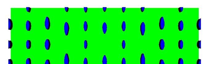
111111 A) IL + Binary Trim                             B) IL + Binary Trim                      '!!![E)IiPSMTri

                     Figure 1: Experimental results of a dual resist IAL process reported by Fritze et al. [2].

(PL). IAL potentially enables 32nm high-resolution patterning with large DOF (Depth of Focus) margin, since IL can print
very high-contrast images. Moreover, unlike IArF (or 157nm) lithography that requires aggressive OPC and continued
increase in mask cost, IAL uses a maskless IL and a low-complexity PL mask. A key challenge to deploy IAL is the
conversion of existing designs to regular-linewidth and regular-pitch layouts. In this paper, we propose and validate a new
IAL-friendly SRAM bitcell design. Despite many theoretical advantages of grid-based regular design techniques, regular
layout of standard logic cells is difficult to deploy, due to large area penalties and electrical performance degradation. An
SRAM bitcell has great significance with respect to RDR, since its circuit topology is relatively easy to place regularly, it
is placed in an array structure, and SRAM occupies a large fraction of SoC die area.
    In this work, we propose a family of grid-based, 1-D regular pitch SRAM bitcell layouts which are amenable to IAL.
Our key contributions are as follows. (1) We suggest a design approach, and specific design rules, for IAL-friendly layouts
of a 6T SRAM bitcell. (2) We provide simulation studies that assess printability of all critical layers (poly, contact, metal,
via) in our proposed bitcell layouts using IAL. (3) We analyze the electrical characteristics, such as SNM, N-curve and
leakage power, of our proposed bitcell layouts drawn with various design rules.
   This paper is organized as follows. Section 2 gives background of the IAL process and SRAM bitcell layout. Section 3
proposes an IAL-friendly bitcell layout scheme, and Section 4 presents the results of lithography simulation and electrical
characteristics for the proposed bitcells. Finally, Section 5 gives conclusions and future research directions.

                                                    2. PRELIMINARIES
2.1. Interference-Assisted Lithography Process
Interference-assisted lithography consists of two exposures – maskless two-beam or four-beam interference lithography
(IL), and projection lithography (PL). IL produces high contrast, regular and high-resolution dense grating patterns, but
this step does not capture detailed circuit geometries. PL is then used to erase a subset of the IL grating patterns so
that only actual design geometries remain on the resist. Figure 1 shows the 32nm design patterns obtained by Fritze et
al. [2] when combining the high-resolution interference with lower-resolution projection lithography. The key advantage
of IAL is the generation of high-contrast images with a maskless step: Since the high-resolution patterns can be generated
without a mask, mask cost is reduced, while mask cost for conventional projection lithography increases continuously
due to optical proximity correction (OPC) complexity. The second exposure that trims unnecessary parts of the grating
patterns can use older-generation projection systems and photomasks which have significantly lower cost.
   The challenge for IAL is to convert existing designs to 1-D regular pitch and regular linewidth. This challenge has
a number of aspects, including resolution limits, required minimum pitch to avoid CD variation during second (trim)
exposure, etc. Requirements for device sizing, reliability and power are also key factors in migration to IAL. Several
central considerations are as follows.
Tradeoff of resolution enhancement vs. cost. IAL can deliver low k1 patterning with larger process window and
lower mask cost. However, IAL is susceptible to overlay error, and incurs many constraints in layout design. We first
compare IAL to existing lithography techniques with respect to the tradeoff of resolution enhancement vs. cost. For 32nm

                                                 Proc. of SPIE Vol. 7122 71221L-2
Figure 2: Problems of IAL application due to metal dummy filling.
half-pitch, there are four candidates that use existing projection illumination. (1) Immersion ArF uses hyper-NA (NA ∼
1.6), but depends on development of fluids with suitable optical and photochemical properties, as well as new photoresists
with higher reflective index. (2) Double dipole exposure is attractive because of the relatively low cost of binary and
attenuated phase shift masks, both of which can be used with dipole illumination. Double dipole exposure splits the
design of two-axis patterns into two separate layers so that two different apertures (i.e., one being x-axis parallel while
the other is the y-axis parallel pole) filter out high diffraction orders for each axis. However, throughput is reduced due to
the double exposure with two different masks. (3) In double patterning lithography (DPL), pitch is effectively managed
using a pattern separation: two patterns with less than required spacing are separated and assigned to two different masks.
While double dipole exposure splits patterns according to pattern direction, DPL improves effective imaging resolution
by splitting a desired pitch into two portions, each with a lower spatial frequency than the original. However, DPL
causes CD variation of neighboring patterns produced in the second exposure, due to topographic effects induced by the
first exposure pattern. (4) AA-PSM enables a smaller circuit feature to have large process margin (depth of focus cross
exposure latitude). The drawback of AA-PSM is that it focuses on the shrinkage of gate length rather than pitch relaxation.
Thus, the technique has application chiefly to high-performance logic devices.
CD variation of neighboring line. CDs of patterns generated by IL can be affected during trim mask exposure, i.e.,
through exposure dose and pattern distortion. An OPC-mediated approach such as biasing the CD of a neighboring line
is not feasible for reducing the impact of such CD variation in IAL. Fritze et al. [3] show that the second PL exposure
produces 20% CD variation when removing a single line and 5% variation when removing two lines. Fundamentally, the
greater the second exposure dose, the greater is its impact on the neighboring CD.
Overlay sensitivity. IAL implementation requires tight overlay control. Fritze et al. [2] simulated double exposure with
15nm overlay range, which may be possible with next-generation equipment. It is reported in [2] that 15nm misalignment
when removing two lines results in a very significant 1.3X dose variation.
Variety of pattern shapes. The drawback of IL is that it can print only one-dimensional regular pitch and linewidth
patterns on a layer. By contrast, today’s typical logic layouts employ a multiplicity of linewidths, pitches and shapes.
On metal layers, CMP dummy fill shapes are required to meet minimum density rules as shown in Figure 2. However,
IAL cannot generate such irregular metal shapes. Moreover, two-dimensional layouts are required for via doubling; the
via landing pad at a metal line-end may requires various linewidths, and non-preferred direction routings (e.g., jogs and
bendings) are used to minimize the number of vias or wirelength. The ubiquity of such metal patterns in modern layouts
can only delay the application of IAL to real devices.
2.2. Rules of Thumb for 6T SRAM Bitcell Design
The 6T SRAM bitcell shown in Figure 3 is composed of six transistors, two bitlines (BL and BLB) and one wordline
(WL). Both bitlines carry complementary data. A bitcell can read or write a bit of data when WL is high. Bitlines are
used for both input and output terminals. The internal six transistors are composed of two pass-gate (PG) transistors (PG1
and PG2), two pull-down (PD) driver transistors (PD1 and PD2) and two pull-up (PU) transistors (PU1 and PU2).
Proc. of SPIE Vol. 7122 71221L-3WL
VDD
PU2
PU1
NR
NL PG2
PG1
PD2
PD1
VSS
BLB BL
Figure 3: Schematic of 6T SRAM bitcell.
Read operation. Before WL goes high, both bitlines are precharged to the supply voltage. When WL goes high, one
of the two bitlines is discharged through a drive transistor. This creates a voltage difference between the bitlines, which
is captured by a sense amplifier attached to the bitlines. Due to the RC timing delay from a bitline capacitance through
a drive transistor to the ground, and to compensate for the mismatch in the sense amplifier, the discharge should be fast
enough for the sense amplifier to realize the voltage difference within a specified time.
Write operation. Write-high and write-low occur at the same time at each internal node, NL and NR. For write-low
operation, when the BL is low, NR is high and W L goes to high, PG2 is turned on and the current flows from VDD through
PU2 and PG2 to BL. At this time, the voltage of NR decreases from the value of the current ratio of PU2 to PG2, and
finally goes to ground when PD2 is turned on by the other internal node, NL.
Reliable operation is a main concern of the bitcell design. A bitcell design must provide stable read, write and data
retention abilities. The two aspects of area and stability are interdependent since designing a bitcell for improved stability
invariably requires a large bitcell area.
Read stability. Read stability means that the data inside a bitcell must not change during the read operation. Data
retention of the SRAM bitcell, both in standby mode and during a read operation, is an important functional constraint.
As explained above, during a read operation discharge must be fast enough and internal node low enough to turn on the
drive transistor of the gate that is connected to that node. Furthermore, once the low state node goes above the inverter
logic threshold voltage, internal data would be changed. The level of voltage increase at the internal node is decided by
the ratio of the current of the drive transistor PD1 (PD2) to that of the access transistor, PG1 (PG2). The current ratio
between drive transistor and access transistor is called the cell-ratio of the SRAM bitcell. Large cell-ratio means a large
drive transistor, so that the voltage on internal node, NL (NR), can be kept as low as the output of the voltage divider of
PD1 (PD2) and PG1 (PG2). For stable read operation, large cell-ratio is preferred, but increases the bitcell area. Usually,
a cell-ratio of 1.5 ∼ 2 minimizes bitcell area while guaranteeing some level of read stability. So, if the gate lengths of
PD1 (PD2) and PG1 (PG2) are the same, the gate width of PD1 (PD2) must be greater than that of PG1 (PG2).
Write ability. Write ability refers to the requirement that data on bitlines must change the internal nodes of the bitcell
within a specified time. This depends on the ratio of currents of the PU1 (PU2) and PG1 (PG2) transistors. To easily
switch the internal node voltage to ground, the current of PG1 (PG2) should be larger than that of PU1 (PU2). This ratio
is called the pull-up ratio, and indicates how easily the data can be changed by the low-state bitline. Pull-up ratio depends
on both PMOS and NMOS currents, hence mobility must be considered during the transistor sizing. If NMOS mobility is
twice PMOS mobility, the same transistor width of PU1 (PU2) and PG1 (PG2) makes the ratio 0.5. So, PU1 (PU2) and
PG1 (PG2) are made as small as possible and can have the same size.
The cell-ratio and pull-up ratio are determined not only by physical layout dimensions but also by the amount of
current for each transistor. In a traditional 6T SRAM bitcell, widths and lengths of transistors are all different to improve
static noise margin (SNM) and to minimize bitcell area. However, in an IAL-friendly design, all six transistors must have
the same gate length. Table 1 shows an example of 32nm bitcell transistor sizing, starting from scaling of an industry
Proc. of SPIE Vol. 7122 71221L-4Diff Poly Cont M1 V1 M2
(a) Initial on-grid layout (b) 1-D regular pitch layout
Figure 4: IAL-friendly bitcell layout.
90nm bitcell. Columns 4 and 5 give the length and width of transistors obtained by naive geometric scaling from 90nm to
32nm. Columns 6 and 7 give the target transistor sizes for an IAL-friendly design.
Table 1: Example of 6T SRAM bitcell device sizing.
TSMC 90nm bitcell 32nm bitcell scaled from 90nm 32nm 1-D regular bitcell
L (nm) W (nm) L (nm) W (nm) L (nm) W (nm)
Pull-Up 100 100 32 32 32 44
Pull-Down 100 175 32 56 32 88
Pass-Gate 115 120 37 38 32 44
Typically, a bitcell’s electrical characteristics are measured by the following static metrics: Butterfly curve [12], N-curve
[4], read current (Iread ), leakage current (Ileakage ), V DDhold , etc. Detailed measurement methods, along with measured
results of the proposed bitcells, are discussed in Section 4 below.
3. IAL-FRIENDLY SRAM BITCELL LAYOUT
As discussed in Section 2.1, all patterns in the IAL-friendly layout must have 1-D regular pitch and linewidth. In this
section, we present an IAL-friendly bitcell layout.
3.1. 1-D Regular Pitch Layout
We generate an initial grid-based bitcell layout as shown in Figure 4(a). We assume that the feature size and minimum
spacing of all layers are each equal to two drawing grids, so that all patterns can have the same linewidth. However, this
grid-based bitcell is still not IAL-friendly, as there exist 2-D patterns on the Metal1 layer; furthermore, not all patterns are
placed on a 1-D pitch, except for poly patterns. All circuit nodes are completely connected using up to the Metal1 layer.
From the initial layout, we can decompact all patterns so that they are placed on the 1-D pitch. However, the ‘L’
shapes on the Metal1 layer cannot be made IAL-friendly through decompaction. To make all geometries 1-D, the ‘L’
shapes must be split into two rectangles, and then one of the rectangles must be moved to another layer, e.g., Metal2. We
use the vertical direction for Metal1 patterns and the horizontal direction for Metal2 patterns. Finally, the new 1-D regular
pitch layout is generated as shown in Figure 4(b).
3.2. Design Rules
To implement a bitcell with 32nm gate length, we must define relevant design rules. In Figure 4(b), we observe that
the IAL-friendly bitcell layout requires at least two poly pitches in the vertical direction, and five contact pitches in the
horizontal direction. The required size of the pitch in each direction is calculated as follows.
Proc. of SPIE Vol. 7122 71221L-5strain layer
spacer Cont
poly poly
poly-to-contact space
poly pitch
Figure 5: Vertical cut-view of SRAM bitcell.
Vertical pitch. Vertical pitch is decided by either minimum IL pitch or the minimum distance that embeds all constituent
materials. Figure 5 shows a vertical cut-view of the proposed bitcell. From the figure, poly pitch must be greater than the
sum of poly width, contact width and twice poly-to-contact spaces. Poly-to-contact space is determined by the sum of the
thickness of spacer and strain layer. Considering certain process variations such as overlay and CD error, poly-to-contact
space is then calculated as
S pc ≥ Wspacer +Wstrain layer + Eoverlay + ECD
where S pc is poly-to-contact space, Wspacer and Wstrain layer are the widths of the spacer and strain layer, and Eoverlay and
ECD are the amounts of overlay error and CD control error. We assume that Wspacer and Wstrain layer are 8nm and 10nm
according to Verhaegen et al. [14], and Eoverlay and ECD are 6.4nm and 2.6nm according to ITRS [6]. Then, the minimum
poly-to-contact space result is 27nm. The required poly pitch is calculated by a simple summation of poly width, contact
width and twice the poly-to-contact space. We also assume that minimum poly width is 32nm and minimum contact
width for 32nm technology is 45nm, following [14]. From this, we see that the poly pitch must be greater than 131nm
(27 × 2 + 32 + 45). Since the expected IL pitch for NA = 1.2 and λ = 193nm is much less than 131nm, vertical pitch is
determined by the above calculation.
Horizontal pitch. In the horizontal direction, there are no constraints analogous to those we saw for vertical pitch (strain
layer, spacer, etc.).∗ Therefore, in the horizontal direction we can use either the same poly pitch size or a reduced pitch
size.
Finally, we define the minimum drawing grid size. Once we determine the number of grids per pitch, we define the
size of a drawing grid by simple arithmetic division and rounding. In the present study, we consider 5 grids per pitch and
6 grids per pitch. If we use 5 grids per pitch, the minimum drawing grid size is 26nm, and if we use 6 grids per pitch, the
minimum drawing grid size is 22nm. Using the minimum drawing grids, we define minimal required design rules to draw
layouts. Table 2 summarizes two sets of design rules corresponding to the two drawing grid sizes.
3.3. Example of IAL-Friendly SRAM Bitcell Layout
Based on the design rules, we develop three different bitcell layouts. In Figure 6, (a) uses the 5-grid rule, (b) uses the
6-grid rule and (c) is also generated by the 6-grid rule but its horizontal pitch is five times the 6-grid rule’s drawing grid.
The bitcell areas are 0.169 um2 , 0.174 um2 and 0.145 um2 , respectively.
Among the bitcells, Figure 6(c) is the best candidate considering area, poly-to-contact space margin, and electrical
characteristics, as we discuss in Section 4. Figure 7 shows the complete layout of each layer of a 25x12 bitcell. All layers
except the diffusion layer have 1-D regular pitch and width.
∗ Horizontal pitch is constrained by the diffusion-to-nwell spacing, diffusion-to-diffusion spacing, and minimum contact/metal/via
pitch (which is in turn determined by IL pitch), etc.
Proc. of SPIE Vol. 7122 71221L-6(a) 25 x10 (b) 30 x12 (c) 25 x12
Figure 6: Three candidate bitcell layouts.
(a) Diffusion and Nwell (b) Poly
(c) Contact (d) Metal1
(e) Via1 (f) Metal2
(g) Via2 (h) Metal3
(i) Via3 (j) Metal4
Figure 7: Layout for each layer.
Proc. of SPIE Vol. 7122 71221L-7Table 2: Two sets of design rules for IAL-friendly layout.
Design rule item 5-grid rule 6-grid rule
Unit drawing grid size 26nm (= 1 grid) 22nm (= 1 grid)
Metal min. width/space 52nm (= 2 grid) 44nm (= 2 grid)
Contact/Via width/space 52nm (= 2 grid) 44nm (= 2 grid)
Diffusion width/space 52nm (= 2 grid) 44nm (= 2 grid)
poly-to-contact space 23nm 28nm
poly pitch 130nm 132nm
4. VALIDATIONS
We evaluate the feasibility of the proposed bitcells in terms of lithography and circuit simulations.
4.1. Lithography Simulation
For lithography simulation, we use Fraunhofer Institute IISB’s Dr. LiTHO version 0.10.5. We use full vector models on
thin mask and high contrast positive 50nm resist model parameters. We apply a simple OPC correction using biasing.
We use a crossquad (XQUAD) setting for block exposure with NA=1.2 of 66nm or 90nm IL pitch. We develop solutions
for all layers except the diffusion layer. We use a positive-tone resist for poly layer and negative-tone resist for all other
layers. Table 3 summarizes our simulation settings for all layers. Consistent with our previous work [11], chromeless
phase assist (CPA) masks provide best-quality block exposure.
Table 3: Lithography simulation conditions.
Mask Type
Layer IL pitch Binary chrome mask Chromeless phase assist Resist type
σCenter σRadial σCenter σRadial
Poly 66nm 0.625 0.15 - - positive
Contact 90nm 0.890 0.15 0.94 0.15 negative
Metal1 90nm 0.890 0.15 0.94 0.15 negative
Via1 90nm 0.410 0.15 - - negative
Metal2 90nm 0.940 0.15 0.94 0.15 negative
Via2 90nm 0.410 0.15 - - negative
Metal3 90nm - - 0.94 0.15 negative
Via3 90nm 0.410 0.15 - - negative
Metal4 90nm - - 0.94 0.15 negative
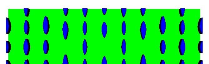
Mask pattern, second exposure image, final exposure image and final resist pattern for poly layer are shown in Figures
8(a), (b), (c) and (d), respectively. Figure 9 shows the resist patterns for contact, Metal1 and Via1 layers. We observe
that all patterns including rectangular contacts and very high dense hole arrays are successfully printed through the IAL
process.
4.2. Circuit Simulation
We verify electrical characteristics of the proposed bitcells according to the following metrics.
Butterfly curve. Butterfly curve is generally used to qualify the static noise margin. To generate the butterfly curve,
we measure the voltage transfer curve between internal nodes, NL and NR. Figure 10 shows the butterfly curves of our
proposed bitcell and the reference bitcell for which transistor sizes are shown in Table 1. We observe that the static noise
margin of our bitcell is similar to that of the reference.
N-Curve. To obtain more insight into static characteristics, the N-curve can be analyzed. The N-curve is generated by
plotting the current consumed by an internal node as the node switches from low to high. SINM (SVNM) is static current
Proc. of SPIE Vol. 7122 71221L-8Blocking Mask (Black = clear)
I I
(a) (b)
250
200 _____ —
1
0 100 200 300 400 500 600
x (nm) Positive resist
(Blue=Resist)
(c) (d)
Figure 8: Lithography simulation results on poly layer imaged using a binary mask.
Negative Resist (Green=Resist)
V V 'V 'V 'V V V
—
Ii 1'&&a&4 ,
p —
p —
_
I£ aI
ItI
p
p
p
p
p
I
&
(a) contact (b) Metal1 (c) Via1
Figure 9. Resist patterns (negative-tone resist) for (a) contact layer, (b) Metal1 layer using CPA-mask and 2-beam IL, and (c) Via1
layer using CPA-mask and 4-beam IL.
Proc. of SPIE Vol. 7122 71221L-91.0 Scaled layout from TSMC90
0.9 (All dimensions are scaled by 0.32) SINM_reg
0.8 SINM_TSMC
0.7
WTV
0.6 1-D regular pitch layout 0.0E+00
SVNM
SINM_TSMC
WTI_TSMC
0.5 SINM_reg
WTI_reg
0.4
0.3 32nm (Scaled from TSMC90)
32nm 1-D regular
0.2
0.1
0.0 -1.0E-04
1 0E 04
0.00
0.07
0.14
0.21
0.28
0.35
0.42
0.49
0.56
0.63
0.70
0.77
0.84
0.91
0.98
0 0.2 0.4 0.6 0.8 1
Figure 10: Butterfly and N-curve comparison for reference and proposed bitcells.
(voltage) noise margin, which is strongly related to read stability; WTI (WTV) is write trip current (voltage), which is
strongly related to write ability. SINM increases and WTI decreases, when the transistor width increases. Larger SINM
means better read ability and smaller WTI means worse write ability. Figure 10 compares N-curves of the proposed bitcell
(SINM reg and WTI reg) and the reference bitcell (SINM TSMC and WTI TSMC). According to the figure, our bitcell
has better read stability but worse write ability.
Iread . Iread is the measured current at a bitline when wordline is switched to high. Large Iread means better read stability.
We observe again that our bitcell has better read stability from the first row of Table 4.
Ileakage . Ileakage is the measured current from the supply node when a bitcell is in stable steady state. Ileakage is important
not only as power consumption itself, but as a metric of stable operation including data retention. Smaller Ileakage is
preferred. However, we observe that our bitcell has larger Ileakage , as seen in the second row of Table 4.
VDDhold . V DDhold is the minimum supply voltage required to hold a bit of data, and is measured by lowering supply
voltage and monitoring the internal nodes. When the voltage difference between NL and NR becomes less than the sensing
margin, the internal data cannot be captured by the sense amplifier and the data will be lost. Comparison of V DDhold in
the third row of Table 4 does not show any significant difference.
Table 4: Comparison of Iread , Ileakage and V DDhold .
Reference (Scaled TSMC) 1-D regular (30x12 and 25x12)
Iread 41.2 uA 66.7 uA
Ileakage 85.4 nA 142.7 nA
V DDhold 110 mV 118 mV
From the simulation results, we conclude that our bitcell has better read stability but worse write ability. However, we
note that since there exists flexibility with respect to diffusion layer patterning, we can further improve write ability by
adjusting diffusion sizes.
Figures 11, 12 and 13 compare the butterfly curve, N-curve, Iread , Ileakage and V DDhold of our three proposed bitcells
across three different operating conditions. Figures 11 and 12 do not show significant degradation of electrical character-
istics, across all operating conditions. We observe that the 25x10 bitcell has the best read stability, but worst write ability,
as we expect from the transistor sizes used in the bitcell. From Figure 13, we again see that the 25x10 bitcell has highest
Iread and highest Ileakage ; V DDhold does not show any difference. We also observe that in all the simulation results, graphs
of the 25x12 bitcell are near-perfectly overlaid by those of the 30x12 bitcell. Therefore, we conclude that the 25x12 bitcell
is the best candidate when considering electrical stability as well as area.
Proc. of SPIE Vol. 7122 71221L-101.20E+00 1.20E+00 1.20E+00
25x10,SS,125degC 25x10,NN,25degC 25x10,FF,Ͳ40degC
1.00E+00 25x12,SS,125degC 1.00E+00
25x12,NN,25degC 1.00E+00
25x12,FF,Ͳ40degC
8.00EͲ01
30x12,SS,125degC 8.00EͲ01 30x12,NN,25degC 8.00EͲ01 30x12,FF,Ͳ40degC
6.00EͲ01 6.00EͲ01 6.00EͲ01
4.00EͲ01 4.00EͲ01 4.00EͲ01
2.00EͲ01 2.00EͲ01 2.00EͲ01
0 00E+00
0.00E+00 0 00E+00
0.00E+00 0 00E+00
0.00E+00
0 0.2 0.4 0.6 0.8 1 1.2 0 0.2 0.4 0.6 0.8 1 1.2 0 0.2 0.4 0.6 0.8 1 1.2
Figure 11: Butterfly curve comparison at different operating conditions.
1.0EͲ04 1.0EͲ04 1.0EͲ04
(SS, 125degC, 1.0V) (NN, 25degC, 1.0V) (FF, -40degC, 1.0V)
5 0E 05
5.0EͲ05 5 0E 05
5.0EͲ05
5.0EͲ05
0.0E+00 0.0E+00
101
101
1
6
1
6
11
16
21
26
31
36
41
46
51
56
61
66
71
76
81
86
91
96
11
16
21
26
31
36
41
46
51
56
61
66
71
76
81
86
91
96
0.0E+00
101
1
6
11
16
21
26
31
36
41
46
51
56
61
66
71
76
81
86
91
96
Ͳ5.0EͲ05 Ͳ5.0EͲ05
Ͳ5.0EͲ05 25x10 25x10 25x10
25x12 Ͳ1.0EͲ04 25x12 Ͳ1.0EͲ04 25x12
30x12 30x12 30x12
Ͳ1.0EͲ04 Ͳ1.5EͲ04 Ͳ1.5EͲ04
Figure 12: N-curve comparison at different operating conditions.
Iread (A) Ileakage (A)
1.80EͲ04 1.00EͲ04
1.60EͲ04 FF,Ͳ4025x10 FF,Ͳ4025x10
1.00EͲ05
1.40EͲ04 FF,Ͳ4025x12 FF,Ͳ4025x12
1.20EͲ04 FF,Ͳ4030x12 1.00EͲ06 FF,Ͳ4030x12
1.00EͲ04 NN,2525x10 NN,2525x10
1.00EͲ07 NN,2525x12
8.00EͲ05 NN,2525x12
NN,2530x12 NN,2530x12
6.00EͲ05 1.00EͲ08
SS 125 25 10
SS,12525x10 SS 125 25x10
SS,12525x10
4.00EͲ05
SS,12525x12 1.00EͲ09 SS,12525x12
2.00EͲ05 SS,12530x12 SS,12530x12
0.00E+00 1.00EͲ10
0.1 0.2 0.3 0.4 0.5 0.6 0.7 0.8 0.9 1 1.1 1.2 1.3 1.4 1.5 VDD (V) 0.1 0.2 0.3 0.4 0.5 0.6 0.7 0.8 0.9 1 1.1 1.2 1.3 1.4 1.5 VDD (V)
(a) Iread (b) Ileakage
VDDhold (V)
0.13
0.128
0.126
0.124
0.122
0.12
0.118
0.116
0.114
0.112
25x10 25x12 30x12 25x10 25x12 30x12 25x10 25x12 30x12
FF, -40 NN, 25 SS, 125
(c) VDDhold
Figure 13: Iread , Ileakage and V DDhold comparison at different operating conditions.
Proc. of SPIE Vol. 7122 71221L-115. CONCLUSIONS AND ONGOING WORK
We have proposed a design methodology for 1-D regular pitch SRAM bitcell layouts which are amenable to an interference-
assisted lithography (IAL) manufacturing process. We derive required design rules for a 6T bitcell to have 32nm gate
length, and propose a family of IAL-friendly bitcell layouts. Through lithography and circuit simulations, we confirm
that the proposed bitcell layouts can be successfully printed by IAL and that their electrical characteristics are comparable
to those of existing bitcell layouts. Our next goals are (1) to provide stronger electrical circuit validation with statistical
analysis and dynamic circuit analysis, including comparison with production SRAM bitcells; (2) to develop a full 1-D
regular pitch bitcell including diffusion layer; and (3) to report measured data that are the results of tapeout.
6. ACKNOWLEDGMENTS
The authors would like to warmly thank Rudi Hendel and Zhilong Rao of Applied Materials, Kevin Liu (formerly of Ap-
plied Materials), and R. Scott Mackay of Petersen Advanced Lithography for their support and many helpful interactions.
Research at UCSD was supported by the Semiconductor Technology Academic Research Center (STARC).
REFERENCES
1. J.-H. Chen et al., “Characterization of ArF Immersion Process for Production”, Proc. SPIE Optical Microlithogra-
phy, 5754 (2005), pp. 13-22.
2. M. Fritze, T. M. Bloomstein, B. Tyrrell, T. H. Fedynyshyn, N. N. Efremow, D. E. Hardy, S. Cann, D. Lennon,
S. Spector and M. Rothschild, “Hybrid Optical Maskless Lithography: Scaling Beyond the 45nm Node”, Journal of
Vacuum Science and Technology B: Microelectronics and Nanometer Structures, 23(6) (2005), pp. 2743–2748.
3. M. Fritze, B. Tyrrel, T. Fedynyshyn and M. Rothschild, “High-Throughput Hybrid Optical Maskless Lithography:
All-Optical 32-nm Node Imaging”, Proc. SPIE Emerging Lithographic Technologies, 5751 (2005), pp. 1058-1068.
4. E. Grossar, M. Stucchi and K. Maex, “Read Stability and Write-Ability Analysis of SRAM Cells for Nanometer
Technologies”, IEEE Journal of Solid-State Circuits, 41(11) (2006), pp. 2577-2588.
5. P. Gupta and A. B. Kahng, “Manufacturing-Aware Physical Design”, Proc. IEEE/ACM Intl. Conference on
Computer-Aided Design, 2003, pp. 681-687.
6. International Technology Roadmap for Semiconductors, http://public.itrs.net/.
7. T. Jhaveri, L. Pileggi, V. Rovner and A. J. Strojwas, “Maximization of Layout Printability/Manufacturability by
Extreme Layout Regularity”, Proc. SPIE Design and Process Integration for Microelectronic Manufacturing, 6156
(2006), pp. 67-81.
8. M. Lavin, F.-L. Heng and G. Northrop, “Backend CAD Flows for Restrictive Design Rules”, Proc. International
Conference on Computer Aided Design, 2004, pp. 739-746.
9. L. Liebmann, D. Maynard, K. McCullen, N. Seong, Ed. Buturla, M. Lavin and J. Hibbeler, “Integrating DfM Compo-
nents Into a Cohesive Design-To-Silicon Solution”, Proc. SPIE Design and Process Integration for Microelectronic
Manufacturing, 5756 (2005), pp. 1-12.
10. W. Maly, Y.-W. Lin and M. Marek-Sadowska, “OPC-Free and Minimally Irregular IC Design Style”, Proc.
ACM/IEEE Design Automation Conference, 2007, pp. 954–957.
11. J. S. Petersen, M. J. Maslow and R. T. Greenway, “An Integrated Imaging System for the 45-nm Technology Node
Contact Holes Using Polarized OAI, Immersion Weak PSM and Negative Resists”, Proc. SPIE Optical Microlithog-
raphy XVIII, 5754 (2005), pp. 488-497.
12. E. Seevinck, F. J. List and J. Lohstroh, “Static-Noise Margin Analysis of MOS SRAM Cells”, IEEE Journal of
Solid-State Circuits, SC-22(5) (1987), pp. 748-754.
13. A. Vanleenhove and D. Van Steenwinckel, “A Litho-Only Approach to Double Patterning”, Proc. SPIE Optical
Microlithography , 6250 (2007), pp. 65202F-1–65202F-10.
14. S. Verhaegen, S. Cosemans, M. Dusa, P. Marchal, A. Nackaerts, G. Vandenberghe and W. Dehaene, “Litho Variations
and Their Impact on the Electrical Yield of a 32nm Node 6T SRAM Cell”, Proc. SPIE Design for Manufacturability
through Design-Process Integration II, 6925 (2008), pp. 69250R-1–69250R-12.
15. J. Wang and A. K. Wong, “Effects of Grid-Placed Contacts on Circuit Performance”, Proc. SPIE Cost and Perfor-
mance in Integrated Circuit Creation, 5043 (2003), pp. 134-141.
16. J. Wang, A. K. Wong and E. Y. Lama, “Standard Cell Design with Regularly-Placed Contacts and Gates”, Proc.
SPIE Design and Process Integration for Microelectronic Manufacturing, 5379 (2005), pp. 56-66.
Proc. of SPIE Vol. 7122 71221L-12You can also read