Simulation of Crystalline Silicon Photovoltaic Cells for Wearable Applications
←
→
Page content transcription
If your browser does not render page correctly, please read the page content below
SPECIAL SECTION ON ENERGY HARVESTING TECHNOLOGIES FOR
                                                                                   WEARABLE AND IMPLANTABLE DEVICES

Received October 30, 2020, accepted December 5, 2020, date of publication January 8, 2021, date of current version February 5, 2021.
Digital Object Identifier 10.1109/ACCESS.2021.3050431

Simulation of Crystalline Silicon Photovoltaic
Cells for Wearable Applications
JINWEI ZHAO 1,2 , (Graduate Student Member, IEEE), ZENGYI XU1 ,
MAN-KAY LAW2 , (Senior Member, IEEE), HADI HEIDARI 1 , (Senior Member, IEEE),
SAMEH O. ABDELLATIF 3 , (Senior Member, IEEE),
MUHAMMAD ALI IMRAN 1 , (Senior Member, IEEE),
AND RAMI GHANNAM 1 , (Senior Member, IEEE)
1 James  Watt School of Engineering, University of Glasgow, Glasgow G12 8QQ, U.K.
2 State Key Laboratory of Analog and Mixed-Signal VLSI, AMSV, University of Macau, Macau 999078, China
3 Electrical Engineering Department, The British University in Egypt, Cairo 11837, Egypt

Corresponding author: Rami Ghannam (rami.ghannam@glasgow.ac.uk)
This work was supported by the UK’s Engineering and Physical Sciences Research Council (EPSRC) under Grant EP/R511705/1.

   ABSTRACT Advancements in the semiconductor industry have enabled wearable devices to be used
   for a wide range of applications, including personalised healthcare. Novel energy harvesting technologies
   are therefore necessary to ensure that these devices can be used without interruption. Crystalline silicon
   photovoltaic (PV) cells provide high energy density to electronic loads. However, the optimization of these
   cells is a complex task since their optical performance is coupled to the surroundings, while their electrical
   performance is influenced by the intrinsic PV characteristics and parasitic losses. Without doubt, simulation
   tools provide the necessary insight to PV cell performance before device fabrication takes place. However,
   the majority of these tools require expensive licensing fees. Thus, the aim of this article is to review the range
   of non-commercial PV simulation tools that can be used for wearable applications. We provide a detailed
   procedure for device modelling and compare the performance of these tools with previously published
   experimental data. According to our investigations, non-commercial 3D tools such as PC3D provide accurate
   simulation results that are only ≈ 1.7% different from their commercial counterpart.

   INDEX TERMS Energy harvesting, photovoltaics, simulation, wearables.

I. INTRODUCTION                                                                                which range from expensive multi-junction semiconductor
According to the late Nobel laureate, Prof. Richard Smal-                                      cells to lower cost non-crystalline cells. In fact, nearly 90%
ley, ‘‘energy is the single most important challenge facing                                    of today’s PV cells are based on crystalline silicon mate-
humanity today’’ [1]. Not only can solar energy help in the                                    rials and innovations in hybrid as well as non-crystalline
democratization of energy, it also has the potential to pro-                                   PV cells are promising improved efficiency and lower cost.
foundly enhance the operation of wearable and implantable                                      However, expensive laboratory facilities and equipment are
devices [2], [3]. Such devices primarily rely on rechargeable                                  often required for the fabrication and characterisation of these
batteries for satisfying their energy needs. However, since                                    cells, which may hinder further research progress in PV
photovoltaic (PV) technology is a mature and reliable method                                   cell development. Furthermore, the insight that comes from
for converting the Sun’s vast energy into electricity, innova-                                 simulations helps designers understand how PV cells perform
tion in developing new materials and solar cell architectures                                  prior to testing, which enables them to make the right product
is becoming more important to increase the penetration of PV                                   design decisions. Consequently, we aim to review the range
technologies in wearable applications.                                                         of experimentally verified multidimensional simulation tools
   A PV cell is a basic device that converts the Sun’s energy                                  that can be used for designing solar cells. These tools allow
into electricity. Currently, a wide variety of PV cells exist,                                 researchers to design and numerically investigate the next
                                                                                               generation of PV cells before fabrication takes place.
    The associate editor coordinating the review of this manuscript and                           The literature provides a wealth of tools for numerically
approving it for publication was Wei E. I. Sha          .                                      simulating PV cells [4]. The earliest simulations involved

                     This work is licensed under a Creative Commons Attribution 4.0 License. For more information, see https://creativecommons.org/licenses/by/4.0/
20868                                                                                                                                                                 VOLUME 9, 2021
J. Zhao et al.: Simulation of Crystalline Silicon PV Cells for Wearable Applications

solving a set of ‘‘continuum’’ partial differential equa-                              simple p-i-n solar cell using a commercial multiphysics FEM
tions, commonly known as the semiconductor equations [5].                              tool. Comparisons between the simulations tools will also
Thanks to early efforts at Bell Labs in the 1960s, com-                                be provided. Towards the end of the article, we will provide
puter simulations demonstrated that PV cell efficiencies can                           recommendations, conclusions and suggestions for further
reach 19% [6], [7]. Improvements in computers enabled these                            work.
simulations to be performed on personal computers (PCs).
Gray and Basore from Purdue University were best known                                 II. STATE OF THE ART
for initiating these modelling efforts during the 1980s and                            The earliest PV FEM modelling tool for solar cells was
early 1990s with their one-dimensional (1D) simulations                                PC1D, as shown from the timeline in Fig. 1. Moreover, a list
programme called PC1D, which solved the semiconductor                                  of free PV modelling tools is shown in TABLE 1.
equations using the finite element method [8]. Later, a more                              For example, PC1D and PC3D are two non-commercial
advanced simulation tool called ‘A Device Emulation Pro-                               tools for 1D and 3D simulations. In the literature, PC1D was
gram and Toolbox’ (ADEPT) was developed, which enabled                                 previously used to optimise the efficiency of a monocrys-
two-dimensional (2D) and three-dimensional (3D) simula-                                talline silicon solar cell with an efficiency of 20.35% [17].
tions to be performed on crystalline-based PV cells [9].                               Similarly, due to its 3D modelling capabilities, PC3D was
Currently, Sentaurus Device is the latest commercial tool for                          used to accurately simulate the optical properties of light
simulating PV cells in 2D and 3D from Synopsis [10]. For                               interacting with the PV cell’s textured surface as well as its
example, the Atwater group in Caltech used this software                               top interdigitated electrode structure [18].
to characterize the performance of nanowire silicon solar                                 General-Purpose Photovoltaic Device Model (GPVDM) is
cells [11].                                                                            another semiconductor simulator that enables users to simu-
   As previously mentioned, crystalline silicon-based solar                            late emerging PV cells, such as perovskite cells. For example,
cells dominate the PV market [10]. Further penetration of                              it was used to investigate the performance of perovskite PV
solar energy solutions in the market relies on develop-                                cells when the active layer thickness and temperature were
ing lower cost cells and improving their efficiency. For                               varied [19]. This tool also provides a 3D graphical representa-
example, increasing the efficiency of solar cells requires                             tion of a PV cell, but only solves the semiconductor equations
innovations in light trapping and in creating antireflection                           in 1D. It has an intuitive output interface that enables users to
coatings [12]–[14]. However, enhancing the performance of                              obtain both electrical and optical PV data, such as the photo
crystalline solar cells is a non-trivial and complex task, since                       absorption rate and the generation rate at different regions
performance relies on ambient conditions, recombination                                within the thickness of the device.
within the semiconductor and various parasitic losses [10].                               Moreover, Analysis of Microelectronic and Photonic
   To predict the performance of solar cells, the finite-                              Structures (AMPS) is another free 1D multipurpose simu-
element-method (FEM) has often been used for solving                                   lations tool, which has been used to investigate the effect
the semiconductor equations describing the electrical carrier                          of varying the absorber layer thickness in Gallium Selenide
properties of solar cells in 1D, 2D or 3D [10]. In the 1D                              (CIGS) PV cells for a range from 300 nm to 3000 nm [20].
and 2D models, carrier generation and optical absorption                               It has a library of monocrystalline, polycrystalline and amor-
are rarely analyzed thoroughly, and only low-dimensional                               phous materials. It can produce Current Density versus
approximations are applied [15]. Since 1D FEM simulations                              Voltage (JV) characteristic curves as well as the quantum
often use the Beer-Lambert method to calculate carrier trans-                          efficiency. However, the tool can only be installed on the
port, 1D tools can be used to simulate basic cells without                             Win XP platform, since its developers do not support newer
features in the direction parallel to the pn-junction [16].                            operating systems nor platforms.
Compared with the optical approximations in 1D modelling,                                 Furthermore, Solar Cell Capacitance Simulator 1D
the electromagnetic (EM) response is calculated using the                              (SCAPS-1D) has been used for modelling polycrystalline Si
Jones matrix method in 2D and 3D, which provides more                                  PV cells [21], perovskite-based PV cells [22] and thin film PV
accurate optical analysis [15].                                                        cells based on Cadmium Telluride (CdTe) [23] and Copper
   According to the literature, 3D software tools enable accu-                         Indium Gallium Selenide (CIGS) [24].
rate simulations that agree with experiments, since para-                                 Automat       for     Simulation     of     Hetero-structures
sitic losses can be included. Some of these parasitic losses                           (AFORS-HET) is another free simulator used to model an
can be considered using the solar cell’s equivalent electri-                           arbitrary 1D sequence semiconductor interface [25]. It has
cal circuit and its subsequent current-voltage (IV) response                           been used to simulate heterojunction PV cells [26]. It can
equation [15]. These losses can be defined in terms of the                             produce both electrical and optical PV data. AFORS-HET
equivalent ‘series’ and ‘shunt’ resistances.                                           can also simulate materials with graded bandgaps as well as
   Nevertheless, the majority of these software tools require                          carrier transport across the various interfaces [27]. However,
expensive licensing fees. Thus, we will review the range of                            it is not capable of simulating high dimensional models of
free software tools for simulating PV cells. We will discuss                           solar cells.
the merits and limitations of these tools. Moreover, we will                              We will compare the performance of these non-commercial
provide a step-by-step demonstration of how to simulate a                              tools with COMSOL, which is a commercial software

VOLUME 9, 2021                                                                                                                                    20869
J. Zhao et al.: Simulation of Crystalline Silicon PV Cells for Wearable Applications
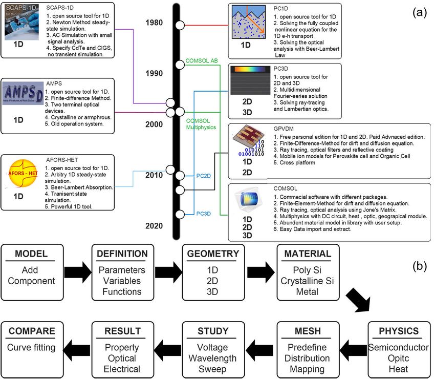
FIGURE 1. (a) Timeline showing the development of four different PV cell simulation tools: PC1D, PC3D, GPVDM and COMSOL.
A comparison between their main features is also shown. (b) Diagram showing the modelling workflow in COMSOL FEM simulation. Briefly,
the tool enables solar cell performance to be predicted by defining the material parameters, geometry, meshing model and other numerical
simulation properties.
program that solves the semiconductor partial differential A. DEFINITION AND SETUP
equation (PDEs) in 1D, 2D and 3D. In addition to its higher Initially, the parameters, variables and functions were set up
dimensional modelling capabilities, COMSOL has an intu- in different scenarios, light intensities and device properties.
itive and easy to use graphical user interface that enables The parameters, functions and variables for the FEM simula-
users to simulate different domains and boundary conditions. tion are summarized in TABLE 2. At first, the electrical prop-
It has been previously used for simulating the performance erties of silicon were defined, which included the intrinsic
of implantable PV cells [2]. Compared with COMSOL, these doping concentration [32], relative permeability [32], elec-
non commercial tools have a smaller file size and are capable tron affinity [32], bandgap [32], density of states [28] and
of solving the semiconductor equations in 1D and 3D. carrier mobility [31].
The density of states and carrier mobility functions are
III. METHODOLOGY shown in Fig. 2(a) and 2(b). The recombination losses will
The following simulation platforms were used during our be determined by the recombination coefficients, such as the
investigations: COMSOL Multiphysics 5.4.0.388 with the Auger coefficient, Radiative coefficient and Shockley-Read-
Semiconductor and Waveoptic modules, PC1D v5.9, PC3D Hall coefficient, which are shown in Fig. 2(c) and 2(d), as well
v1.7 and AFORS-HET v2.5. The simulations were per- as TABLE 2.
formed on a computer with an Intel Core i5-6300U processor The absorption of light and generation of an electron-hole
(2.40 GHz), 4 GB RAM and a Windows 10 64-bit operating pair is fundamental to PV cell operation. In this process,
system. the energy of a photon is initially converted to electrical
20870 VOLUME 9, 2021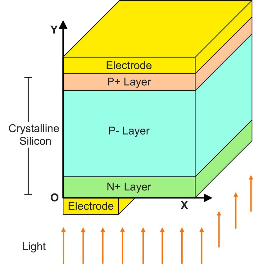
J. Zhao et al.: Simulation of Crystalline Silicon PV Cells for Wearable Applications

TABLE 1. Comparison Between Different Simulation Tools.

     FIGURE 2. (a) Density of states model from Couderc et al. 2014 [28]. (b) Carrier mobility parameterization from Klaassen et al. 1987 [10].
     (c) Auger coefficients of Dziewior and Schmid, which were obtained from P. Altermatt et al. 2011 [10]. (d) Radiative recombination coefficient
     from Nguyen et al. 2014 [29]. (e) Refractive index of crystalline Silicon from Aspnes et al. 1983 [30]. (f) Photon flux density of AM1.5G spectrum
     from Nguyen et al. 2014 [29].

energy through the creation of an electron-hole pair [4]. The                          and parameters are summarised in TABLE 3. We used these
refractive index of silicon was used to analyse the amount                             parameters to compare the performance of our simulations
of light absorbed or penetrated in the PV cell, as shown                               tools with experimental data from two different sources [33]
in Fig. 2(e).                                                                          and [34].
   Moreover, for simulating the performance of PV cells,                                 In our simulations, light penetrates from the bottom of the
the AM1.5G global irradiance spectrum was used, where a                                cell with an incident angle of zero, as shown in figure 3.
power density of 1000 W /cm2 was assumed. The photon flux                              Therefore, the front surface of the cell was located at y = 0.
spectrum shown in Fig. 2(f) was used to set up the generation                          Moreover, two metal contact were added to the front and rear
rate [29]. Unless otherwise stated, an ambient temperature                             surface of the PV cells.
of 300 K was used [32].
                                                                                       C. MATERIAL ALIGNMENT
B. GEOMETRY DESIGN                                                                     Polycrystalline silicon was used as the device material, with
Simulating an ideal p-i-n junction diode requires a uniform                            the properties shown in TABLE 2. An ‘air’ layer was defined
doping profile in each region. In our simulations, we have                             on the top and bottom sides of the PV cell with a refractive
defined the different layers as heavy n-type doped (N+), light                         index of (NAir = 1.0003) [35]. Since the doping concen-
p-type doped (P-) and heavy p-type doped (P+). The length                              tration is different in each layer, parameters such as carrier
of these layers was Lp+ , LN + , and LP− . The device properties                       mobility and recombination coefficient are different. In this

VOLUME 9, 2021                                                                                                                                        20871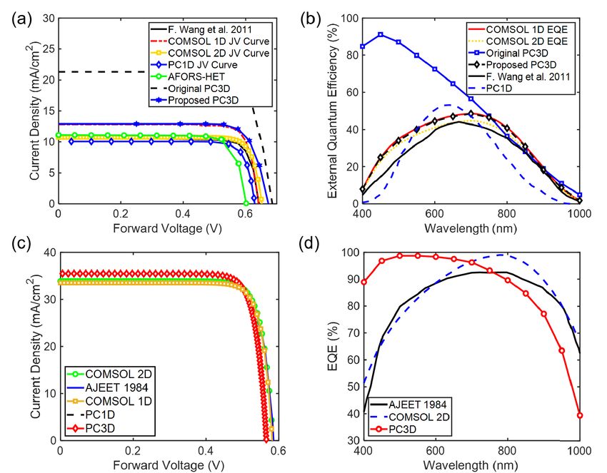
J. Zhao et al.: Simulation of Crystalline Silicon PV Cells for Wearable Applications

TABLE 2. Summary of Device Simulation Parameters.

                                                                  FIGURE 3. Structure and architecture of the experimental PV devices
                                                                  in [33] and [34]. For comparison, we simulated the same structure using
                                                                  COMSOL as well as the non-commercial software programmes.

                                                                                 q
TABLE 3. Devices Properties.                                           12 φ =        (n − p − ND + NA )                        (3)
                                                                               ε0 εr
                                                                  where n and p are the electron and hole concentrations, Dn
                                                                  is the electron diffusion coefficient, Dp is the hole diffusion
                                                                  coefficient, µn is the electron mobility, µp is hole mobility, k
                                                                  is the Boltzmann’s constant, T = 300 K is the operating tem-
                                                                  perature, q is the electronic charge and φ is the electrostatic
                                                                  potential. χ is the electron affinity and Eg is the bandgap.
                                                                  Nc (Nv ) is the effective conduction (valence) band density,
                                                                  R is the carrier recombination rate and G is the generation
                                                                  rate. Furthermore, 0 and r are the permittivity of free space
                                                                  and the relative permittivity of crystalline silicon. ND and
case, the materials were set up differently and aligned to        NA are the ionized donor and acceptor concentrations. The
specific layers (N+, P− and P+) with different doping con-        recombination consists of the Shockley-Read-Hall, Radiative
centrations Np+ , NN + , and NP− .                                and Auger recombinations [10]:

D. PHYSICAL MODEL DESCRIPTION                                                           R = RSRH + Rrad + Raug                                  (4)
To analyze carrier transport across the heterojunction inter-                                       np − n2i
                                                                                    RSRH =                                                      (5)
faces, the semiconductor module enables important semi-                                     τn (p + pt ) + τp (n + nt )
conductor function definition, such as doping, generation,
                                                                                     Rrad = Brad np − n2i                                       (6)
recombination, trap density and space charge density. On the
other hand, PC1D, GPVDM and AFORS-HET enable users
                                                                                     Rang = Cn n + Cp p np − n2i                                (7)
to customize the doping concentration and diffusion length,
while PC3D enables users to define the doping concentration       where pt and nt are the hole and electron trap concentrations.
by changing the sheet resistance of each layer. The equations     In fact, highest RSRH are achieved when nt = pt = ni .
solved by the simulations programs are: [5], [10], [15]:          Moreover, Brad is the radiative coefficient, Cn and Cp are the
                                                                  Auger coefficients for electron and holes, τp and τn are the
                                 1χ

                                        kT
     1 −Dn 1n + nµn 1φ +              +     1 ln Nc               recombination lifetimes of electrons and holes.
                                  q      q                           Similarly, the generation rate is expressed in terms of:
         = G (x, y, z, λ) − R                             (1)

                              1χ 1Eg kT
                                                                                              G = αN0 e−αy                                    (8)
     1 −Dp 1p+pµp 1φ +            +       − 1 ln Nc
                               q      q      q                    where N0 is the photon flux at the surface (shown in Fig. 3(f)),
         = G(x, y, z, λ) − R                              (2)     α is the absorption coefficient (α = 4π Si(k)/λ, where Si(k)

20872                                                                                                                               VOLUME 9, 2021
J. Zhao et al.: Simulation of Crystalline Silicon PV Cells for Wearable Applications

is the imaginary part of refractive index shown in Fig. 2(e)),                         using:
and y is the distance into the material.
                                                                                                 Jn = −qµn n∇ψ − qDn ∇n                            (15)
E. OPTICAL CALCULATIONS                                                                          Jp = −qµp p∇ψ − qDp ∇p                            (16)
                                                                                                      ZZZ
To determine the optical characteristics in 2D, the 2× 2 Jones                                  Jsc =       Jn (x, y, λ) + Jp (x, y, λ) dx.dy.dλ   (17)
Matrix method was used [30]:
                   m
                      "                    #

         ERa
              X
                         cos ϕi ηji sin ϕi       1                                     Considering the parasitic resistances, the output current den-
               =                                           (9)                         sity of the PV cell can be obtained using:
         BRa              jηi sin ϕi cos ϕt      ηm
                  i=1
                                                                                                                   − VV             V +J (V )Rs
where δi is the wave phase shift (δi = 2πNi di cosθi/λ) in the                                       J (V ) = −J0 e   T   + Jsc −      Rsh         (18)
ith layer, Ni is the refractive index, di is the thickness of the                      where Rs and Rsh are the series and shunt parasitic resistances,
ith layer, ηi is the pseudo index in ith layer (ηi = Ni cosθi ).                       and VT is the thermal voltage (VT = kT /q). Since our
ERa or BRa is the ratio between the electric and magnetic                              simulations model is in 2D, Rs can be neglected and Rsh can
fields of the transmitted light and incident light. M is the                           be calculated using the current-voltage (IV) characteristics of
total number of layers. The reflectance (R), absorptance (A)                           the device. The External Quantum Efficiency (EQE) can be
transmittance (T = 1 − A − R) of light can be determined                               determined using:
using:                                                                                                                  hcJsc
                              4η0 Re (ηm )                                                                   EQE =                                 (19)
             R=                                              (10)                                                      qλIrad
                     η0 ERa + BBn (η0 ERa + BRa )∗

                                                                                       where h is the Plank constant, c is the speed of light, Irad is
                         4η0 Re ERa B∗Ra − ηm

                                                                                       the irradiance under AM 1.5G.
             A=                                              (11)
                     η0 ERa + BB0 (η0 ERa + BRa )∗

                                                                                       G. SEMICONDUCTOR AND SIMULATION SETUP
1) INITIAL CONDITION SETUP                                                             In PC1D, GPVDM and AFORS-HET, the doping concentra-
Initially, we applied the neutral charge condition to setup the                        tion and diffusion length in each semiconductor layer need to
doping profile and ohmic contact characteristics for estimat-                          be defined. However, in PC3D the setting are different, since
ing the initial electrostatic potential. The initial doping pro-                       the relative doping concentrations need to be converted into a
files for p-type (pinit ) and n-type (ninit ) doping were defined                      sheet resistance. The doping profile were set according to the
by applying the neutral charge condition, where ninit − pinit −                        parameters given in TABLE 3.
C = 0 and ninit pinit = n2i . These can be described in terms                             In the PC1D, PC3D, GPVDM and AFORS-HET, only the
of:                                                                                    surface recombination can be customized, while COMSOL
                                                                                       enables users to define different types of recombination.
                             q
                           1       2      2
                 ninit =         C + 4ni + C                  (12)                     Moreover, PC1D, PC3D, GPVDM and AFORS-HET enable
                           2
                           1
                             q                                                       users to change the irradiance settings as well as the surface
                 pinit =         C 2 + 4n2i − C               (13)                     reflection.
                           2
                                                                                          In COMSOL, two types of doping profiles can be defined,
                           kT           C
                8init =       arcsin h                        (14)                     which are ‘gradient’ and ‘uniform’. To ensure consistency
                            q          2ni                                             with the non-commercial tools, we have used the ‘uniform’
This initial electrostatic potential can be estimated for ohmic                        doping in PC1D, PC3D, GPVDM and AFORS-HET as well
contacts. It can also predict the initial potential profile and the                    as COMSOL. Then, the generation function was set to excite
doping profile in a homojunction.                                                      the electron-hole pairs in the device. Furthermore, in the
                                                                                       COMSOL programme three types of recombination were
2) BOUNDARY CONDITIONS                                                                 defined by invoking eqs. 4-7.
Periodic boundary conditions were used in the transverse                                  Since the doping concentration is high in the heavily doped
directions for both carrier diffusion and electrostatic poten-                         regions (N+ and P+), the bandgap narrowing functionality
tial. Along the junction interface, surface recombination con-                         in COMSOL was used. Next, two metal contacts (Anode and
ditions were used for the carrier diffusion modules. For                               Cathode) were defined to complete the PV cell architecture.
the Poisson equations under forward bias, the cathode was                              Moreover, when selecting a ‘Terminal Type‘, there were four
grounded and unchanged, but the voltage at the anode was                               available options in COMSOL, which were Charge, Volt-
varied from an initial value of zero to the forward bias voltage.                      age, Circuit, or Terminated. In this case, we selected ‘Volt-
In COMSOL and AFORS-HET, the boundary conditions can                                   age’. Finally, for ‘Contact Type’ we selected ‘Ideal Ohmic’.
be customized.                                                                         To complete our analysis of these PV cells, we investigated
                                                                                       their performance with respect to voltage as well as forward
F. ELECTRICAL OUTPUT CHARACTERISTIC                                                    biasing voltage. We therefore varied the voltage between
First, the electron current density (Jn ), hole current density                        0 and 0.7 V, whereas the wavelength range was 400ñm <
(Jp ) and short-circuit current density (Jsc ) can be determined                       λ < 1000 nm.

VOLUME 9, 2021                                                                                                                                     20873
J. Zhao et al.: Simulation of Crystalline Silicon PV Cells for Wearable Applications

        FIGURE 4. (a) Comparison between the simulation results from PC1D, PC3D (original and proposed), COMSOL, AFORS-HET and
        experimental data from F. Wang et al. 2011 [33]. (b) External Quantum Efficiency results from PC1D, PC3D, COMSOL 1D, COMSOL 2D
        and experimental data from F. Wang et al. 2011 [33]. (c) Comparison between simulation results from PC1D, PC3D, COMSOL 2D and
        experimental data from A. Rohatgi et al. 1984 [34]. (d) External Quantum Efficiency results from PC1D, PC3D, COMSOL 2D and
        experimental data from A. Rohatgi et al. 1984 [34].

IV. RESULTS AND DISCUSSION                                                   Based on these simulation results, PC1D can be regarded
We compared our simulation results with experimental data                 as a reliable software tool that agrees with experiments.
from [33], [34], [36]. The PV cell properties were provided               This is perhaps why it has been regularly used by the PV
in TABLES 2 and 3. As previously mentioned, the modeled                   industry for decades. With COMSOL 1D and 2D, there are
solar cell consists of five stacked layers, which are air, a layer        plenty of library resources and multi-physics modules that
of N+ silicon, an intrinsic layer, P+ layer, followed by                  can facilitate the modelling of different materials and device
another layer of air. A comparison between the JV curves                  architectures. Furthermore, numerical solutions to the PV
for the simulation programmes is shown in Fig. 4. Despite                 equations were achieved in less than 5 s with COMSOL 1D,
using the parameters, the simulations tools provided different            while the 2D COMSOL simulations needed 10 − 30 s.
results. We will discuss which tools provided better agree-                  With AFORS-HET, our PV cell modelling achieved Jsc =
ment with experimental data.                                              11 mA/cm2 and Voc = 0.6 V , which compares favourably
   Clearly, the simulation results from COMSOL 2D and                     with experimental as well as the COMSOL data. In fact,
PC1D are closely matched to experimental data. However,                   AFORS-HET is useful since it allows the user to define
results from COMSOL 1D are different from experimen-                      different interface materials and boundary conditions. These
tal data. In fact, there is almost a 2 mA/cm2 difference in               functionalities are not available in the other surveyed 1D
Jsc ), as shown in Fig. 4(a). We believe that this could be               simulation tools.
attributed to the optical approximation invoked by using the                 As shown from Fig. 4(a), PC3D provides slightly different
Beer-Lambert Law. Despite the difference in Jsc , the Voc data            results. Initially, Jsc = 21.3 mA/cm2 and Voc = 0.69 V . This
from PC1D as well as COMSOL 1D and 2D all agree with                      large difference in results was due to using the default spectral
experimental data (0.64 V ).                                              transmission parameters in PC3D, where no reflectance was

20874                                                                                                                                       VOLUME 9, 2021
J. Zhao et al.: Simulation of Crystalline Silicon PV Cells for Wearable Applications

assumed. However more accurate results can be obtained by                              environmental effects. In this case, PC3D is an alternative
modifying the optical parameters. As previously mentioned,                             and free option that can perform many of COMSOL’s simula-
the front spectral reflectance was set to 70% [37] and the back                        tions, provided that devices are larger than 1µm. This is also
reflectace was set to 50% [38], which enabled the EQE results                          especially true if the device properties library is complete,
to match those from COMSOL 1D, as shown in Fig. 4(b).                                  with an ability to modify the optical properties. We can also
Thus, an improved curve with Jsc = 12.9 mA/cm2 and Voc =                               obtain more accurate results if multi-physics simulations can
0.67 V was obtained.                                                                   be involved, where the effects of temperature and stress can
   With PC3D, the software can only simulate devices with                              be investigated.
thicknesses exceeding 1µm. This is an important limitation,
especially for wearable PV devices, where thin film mate-                              V. CONCLUSION
                                                                                       In this article we provided a review of the different non-
rials are now attracting interest. For the sake of comparison,
                                                                                       commercial software tools for simulating PV cells that can
the experimental device in [33] is 20% smaller than this limit,
                                                                                       be used in wearable applications. In total, we reviewed
whereby the thickness of the PV cell was 800 nm. Naturally,
                                                                                       five different software programmes. We also provided a
since the simulated PV cell is thicker than the experimental
                                                                                       detailed procedure for simulating a p-i-n solar cell using a
cell in [33], the Jsc = 12.9 mA/cm2 , which is larger than the
                                                                                       set of predefined solar cell parameters. Using these param-
Jsc reported in [33] (10.5 mA/cm2 ). Consequently, there is a
                                                                                       eters, we subsequently compared these simulation results
−22.9% difference between these experimental and simula-
                                                                                       with a commercial, multiphysics simulations program called
tion Jsc results.
                                                                                       COMSOL, which solves the semiconductor equations using
   Due to this limitation with PC3D, we have also inves-
                                                                                       the finite element method (FEM). According to our inves-
tigated a thicker PV cell with a thickness of 150 µm),
                                                                                       tigations, all simulation tools provided different results.
as reported in [34]. From our simulation results in PC3D,
                                                                                       This was due to their differing approaches for solving the
Jsc = 35.5 mA/cm2 , which is much closer to the experimental
                                                                                       semiconductor equations. Nevertheless, we concluded that
results mentioned in [34] (Jsc = 36.1 mA/cm2 ), as can be
                                                                                       PC3D is the most accurate non-commercial tool for wear-
verified from the results in Fig. 4(c). Therefore, the differ-
                                                                                       able applications, since their results closely match the data
ence between the experimental and simulation results is now
                                                                                       from COMSOL, particularly since the data also agreed with
only 1.7%.
                                                                                       previously published experiments.
   As for the External Quantum Efficiency (EQE) results
shown in Fig 4(b) and (d), COMSOL shows better agreement                               REFERENCES
with experimental data compared with PC1D and PC3D.                                     [1] US Senate Committee on Energy and Natural Resources. (2020). Tran-
The mismatch in results is mainly due to the material and                                   script of the Testimony of Richard E. Smalley to the US Senate Committee
                                                                                            on Energy and Natural Resources. Accessed: Oct. 9, 2020. [Online]. Avail-
optical properties setup in these programs. For example,                                    able: https://www.gpo.gov/fdsys/pkg/CHRG-108shrg95239/html/CHRG-
in COMSOL three types of recombination can be defined,                                      108shrg95239.%htm
which are Radiative, Auger and Schockley-Read-Hall recom-                               [2] J. Zhao, R. Ghannam, M.-K. Law, M. A. Imran, and H. Heidari, ‘‘Photo-
                                                                                            voltaic power harvesting technologies in biomedical implantable devices
bination. On the other hand, in PC1D and PC3D only sur-                                     considering the optimal location,’’ IEEE J. Electromagn., RF Microw. Med.
face and bulky recombination can be defined. Furthermore,                                   Biol., vol. 4, no. 2, pp. 148–155, Jun. 2020.
in PC3D the EQE is usually calculated using the previously                              [3] J. Zhao, R. Ghannam, K. O. Htet, Y. Liu, M.-K. Law, V. A. Roy, B. Michel,
                                                                                            M. A. Imran, and H. Heidari, ‘‘Self-powered implantable medical devices:
mentioned default optical parameters. Including the front                                   Photovoltaic energy harvesting review,’’ Adv. Healthcare Mater., vol. 9,
and back spectral reflectance leads to better agreement with                                no. 17, 2020, Art. no. 2000779.
experimental data, as shown from the ‘Proposed PC3D’ curve                              [4] P. Altermatt, Numerical Simulation of Crystalline Silicon Solar
                                                                                            Cells. Hoboken, NJ, USA: Wiley, 2016, ch. 3.8, pp. 150–159.
results in figure 4. Consequently, this proves that the PC3D                                [Online]. Available: https://onlinelibrary.wiley.com/doi/abs/10.1002/
simulation results can be setup to show good agreement with                                 9781118927496.ch15
experimental data.                                                                      [5] W. Van Roosbroeck, ‘‘Theory of the flow of electrons and holes in ger-
                                                                                            manium and other semiconductors,’’ Bell Syst. Tech. J., vol. 29, no. 4,
   Clearly, COMSOL is a software tool with a vast materials                                 pp. 560–607, Oct. 1950.
library, great curve fitting features and a multiphysics envi-                          [6] J. G. Fossum, ‘‘Computer-aided numerical analysis of silicon solar cells,’’
ronment, which produces results that agree with experimen-                                  Solid-State Electron., vol. 19, no. 4, pp. 269–277, Apr. 1976.
                                                                                        [7] J. G. Fossum, ‘‘Physical operation of back-surface-field silicon solar
tal data. It can therefore be used to accurately predict the                                cells,’’ IEEE Trans. Electron Devices, vol. 24, no. 4, pp. 322–325,
performance of PV cells for wearable applications, partic-                                  Apr. 1977.
ularly when such cells are exposed to non-uniform lighting                              [8] P. A. Basore, ‘‘Numerical modeling of textured silicon solar cells using PC-
                                                                                            1D,’’ IEEE Trans. Electron Devices, vol. 37, no. 2, pp. 337–343, Feb. 1990.
conditions. In that case, the 3D PV cell model can be used to                           [9] J. L. Gray, ‘‘ADEPT: A general purpose numerical device simulator for
investigate the change in irradiance along the horizontal and                               modeling solar cells in one-, two-, and three-dimensions,’’ in Proc. Conf.
vertical axes. Secondly, wearable applications require highly                               Rec. 22nd IEEE Photovoltaic Spec. Conf., Oct. 1991, pp. 436–438.
                                                                                       [10] P. P. Altermatt, ‘‘Models for numerical device simulations of crystalline
flexible devices for improved user comfort. In 3D modelling,                                silicon solar cells—A review,’’ J. Comput. Electron., vol. 10, no. 3,
it is easier to analyze the stress and pressure inside the                                  pp. 314–330, Sep. 2011.
device. Eventually, the PV cell semiconductor model in 3D                              [11] M. D. Kelzenberg, M. C. Putnam, D. B. Turner-Evans, N. S. Lewis,
                                                                                            and H. A. Atwater, ‘‘Predicted efficiency of Si wire array solar cells,’’
COMSOL can be easily integrated with other multi-physics                                    in Proc. 34th IEEE Photovoltaic Spec. Conf. (PVSC), Jun. 2009,
modules to investigate the impact of heat, pressure and other                               pp. 001948–001953.

VOLUME 9, 2021                                                                                                                                                   20875
J. Zhao et al.: Simulation of Crystalline Silicon PV Cells for Wearable Applications

[12] H. A. Atwater, ‘‘Seeing the light in energy use,’’ Nanophotonics, vol. 10,         [33] F. Wang, H. Yu, J. Li, S. Wong, X. W. Sun, X. Wang, and H. Zheng,
     no. 1, pp. 115–116, Dec. 2020. [Online]. Available: https://www.degruyter.              ‘‘Design guideline of high efficiency crystalline Si thin film solar cell with
     com/view/journals/nanoph/10/1/article-p115.xml                                          nanohole array textured surface,’’ J. Appl. Phys., vol. 109, no. 8, Apr. 2011,
[13] S. Abdellatif, K. Kirah, R. Ghannam, A. S. G. Khalil, and W. Anis,                      Art. no. 084306.
     ‘‘Enhancing the absorption capabilities of thin-film solar cells using             [34] A. Rohatgi and P. Rai-Choudhury, ‘‘Design, fabrication, and analysis of
     sandwiched light trapping structures,’’ Appl. Opt., vol. 54, no. 17,                    17-18-percent efficient surface-passivated silicon solar cells,’’ IEEE Trans.
     pp. 5534–5541, Jun. 2015. [Online]. Available: http://ao.osa.org/abstract.              Electron Devices, vol. 31, no. 5, pp. 596–601, May 1984.
     cfm?URI=ao-54-17-5534                                                              [35] P. E. Ciddor, ‘‘Refractive index of air: New equations for the visible and
[14] S. Abdellatif, R. Ghannam, and A. S. G. Khalil, ‘‘Simulating the dispersive             near infrared,’’ Appl. Opt., vol. 35, no. 9, pp. 1566–1573, 1996.
     behavior of semiconductors using the lorentzian-drude model for photo-             [36] S. M. Wong, H. Y. Yu, Y. Li, J. Li, X. W. Sun, N. Singh, P. G. Q. Lo,
     voltaic devices,’’ Appl. Opt., vol. 53, no. 15, pp. 3294–3300, May 2014.                and D.-L. Kwong, ‘‘Boosting short-circuit current with rationally designed
     [Online]. Available: http://ao.osa.org/abstract.cfm?URI=ao-53-15-3294                   periodic Si nanopillar surface texturing for solar cells,’’ IEEE Trans. Elec-
[15] X. Li, N. P. Hylton, V. Giannini, K.-H. Lee, N. J. Ekins-Daukes, and                    tron Devices, vol. 58, no. 9, pp. 3224–3229, Sep. 2011.
     S. A. Maier, ‘‘Multi-dimensional modeling of solar cells with electromag-          [37] J. Humlíček and K. Vojtěchovský, ‘‘Infrared optical constants of N-type
     netic and carrier transport calculations,’’ Prog. Photovoltaics, Res. Appl.,            silicon,’’ Czechoslovak J. Phys., vol. 38, no. 9, pp. 1033–1049, Sep. 1988.
     vol. 21, no. 1, pp. 109–120, Jan. 2013.                                            [38] S. Strehlke, S. Bastide, and C. Lévy-Clément, ‘‘Optimization of porous
[16] J. Nelson, The Physics of Solar Cells. London, U.K.: Imperial College                   silicon reflectance for silicon photovoltaic cells,’’ Sol. Energy Mater. Sol.
     Press, 2003.                                                                            Cells, vol. 58, no. 4, pp. 399–409, Aug. 1999.
[17] G. Hashmi, A. R. Akand, M. Hoq, and H. Rahman, ‘‘Study of the
     enhancement of the efficiency of the monocrystalline silicon solar cell by
     optimizing effective parameters using PC1D simulation,’’ Silicon, vol. 10,
     no. 4, pp. 1653–1660, Jul. 2018.
[18] P. A. Basore, ‘‘Efficient computation of multidimensional lambertian opti-
     cal absorption,’’ IEEE J. Photovolt., vol. 9, no. 1, pp. 106–111, Jan. 2019.                                 JINWEI ZHAO (Graduate Student Member,
[19] H. Abdulsalam, G. Babaji, and H. T. Abba, ‘‘The effect of temperature and                                    IEEE) received the B.Eng. degree in electrical and
     active layer thickness on the performance of ch3nh3pbi3 perovskite solar                                     electronics engineering from The University of
     cell: A numerical simulation approach,’’ J. Found. Appl. Phys., vol. 5, no. 2,                               Edinburgh, in 2016, and the M.Sc. degree in elec-
     pp. 141–151, 2018.                                                                                           tric power from Newcastle University, U.K., 2017.
[20] J. Ray, C. Panchal, M. Desai, and U. Trivedi, ‘‘Simulation of CIGS thin                                      He is currently pursuing the Ph.D. degree with
     film solar cells using amps-1D,’’ J. Nano-Electron. Phys., vol. 3, no. 1,                                    the University of Glasgow. He participated in the
     pp. 747–754, 2011.                                                                                           FDCT (The Science and Technology Development
[21] M. Burgelman, P. Nollet, and S. Degrave, ‘‘Modelling polycrystalline                                         Fund) funded project ‘‘High Efficiency Energy
     semiconductor solar cells,’’ Thin Solid Films, vols. 361–362, pp. 527–532,                                   Harvesting System for Biomedical Devices’’ and
     Feb. 2000.                                                                         exchanged to the State Key Laboratory of Analog and Mixed-Signal VLSI
[22] S. Bansal and P. Aryal, ‘‘Evaluation of new materials for electron and hole        Group, University of Macau, in 2019. His research interests include energy
     transport layers in perovskite-based solar cells through SCAPS-1D simu-            harvesting, implantable systems, and photovoltaic cells.
     lations,’’ in Proc. IEEE 43rd Photovoltaic Spec. Conf. (PVSC), Jun. 2016,
     pp. 0747–0750.
[23] C.-H. Huang and W.-J. Chuang, ‘‘Dependence of performance parameters
     of CdTe solar cells on semiconductor properties studied by using SCAPS-
     1D,’’ Vacuum, vol. 118, pp. 32–37, Aug. 2015.
[24] M. Mostefaoui, H. Mazari, S. Khelifi, A. Bouraiou, and R. Dabou, ‘‘Sim-                                        ZENGYI XU is currently pursuing the B.Eng.
     ulation of high efficiency CIGS solar cells with SCAPS-1D software,’’                                          degree in electrical and electronic engineering
     Energy Procedia, vol. 74, pp. 736–744, Aug. 2015.                                                              from the University of Glasgow. In the summer
[25] A. Froitzheim, R. Stangl, L. Elstner, M. Kriegel, and W. Fuhs, ‘‘AFORS-                                        of 2020, he participated in the research project of
     HET: A computer-program for the simulation of heterojunction solar cells                                       Energy harvesting at the University of Glasgow.
     to be distributed for public use,’’ in Proc. 3rd World Conf. Photovoltaic                                      During that research experience, he obtained valu-
     Energy Convers., vol. 1, May 2003, pp. 279–282.                                                                able knowledge of team cooperation and funda-
[26] M. Ghannam and Y. Abdulraheem, ‘‘Electro-physical interpretation of the                                        mental skills in semiconductor simulation. His
     degradation of the fill factor of silicon heterojunction solar cells due to                                    current interests include optical communication,
     incomplete hole collection at the a-Si:H/c-Si thermionic emission barrier,’’
                                                                                                                    photovoltaic device, and light emitting diode.
     Appl. Sci., vol. 8, no. 10, p. 1846, Oct. 2018.
[27] M. Riaz, A. C. Kadhim, S. K. Earles, and A. Azzahrani, ‘‘Variation in
     efficiency with change in band gap and thickness in thin film amorphous
     silicon tandem heterojunction solar cells with AFORS-HET,’’ Opt. Exp.,
     vol. 26, no. 14, p. A626, 2018.
[28] R. Couderc, M. Amara, and M. Lemiti, ‘‘Reassessment of the intrinsic                                          MAN-KAY LAW (Senior Member, IEEE) received
     carrier density temperature dependence in crystalline silicon,’’ J. Appl.                                     the B.Sc. degree in computer engineering and the
     Phys., vol. 115, no. 9, Mar. 2014, Art. no. 093705, doi: 10.1063/1.4867776.                                   Ph.D. degree in electronic and computer engineer-
[29] H. T. Nguyen, S. C. Baker-Finch, and D. Macdonald, ‘‘Temperature                                              ing from The Hong Kong University of Science
     dependence of the radiative recombination coefficient in crystalline silicon                                  and Technology (HKUST), in 2006 and 2011,
     from spectral photoluminescence,’’ Appl. Phys. Lett., vol. 104, no. 11,                                       respectively. In February 2011, he joined as a
     Mar. 2014, Art. no. 112105.                                                                                   Visiting Assistant Professor with HKUST. He is
[30] D. E. Aspnes and A. A. Studna, ‘‘Dielectric functions and optical parame-
                                                                                                                   currently an Assistant Professor with the State Key
     ters of Si, ge, GaP, GaAs, GaSb, InP, InAs, and InSb from 1.5 to 6.0 eV,’’
                                                                                                                   Laboratory of Analog and Mixed-Signal VLSI,
     Phys. Rev. B, Condens. Matter, vol. 27, no. 2, pp. 985–1009, Jan. 1983,
     doi: 10.1103/PhysRevB.27.985.
                                                                                                                   Faculty of Science and Technology, University of
[31] P. P. Altermatt, J. O. Schumacher, A. Cuevas, M. J. Kerr, S. W. Glunz,             Macau, Macau, China. He has authored or coauthored more than 80 tech-
     R. R. King, G. Heiser, and A. Schenk, ‘‘Numerical modeling of highly               nical publications and six U.S./Chinese patents. He has developed world-
     doped Si:P emitters based on Fermi–Dirac statistics and self-consistent            leading ultra-low power CMOS temperature/image sensing systems, and
     material parameters,’’ J. Appl. Phys., vol. 92, no. 6, pp. 3187–3197,              fully integrated high efficiency solar/ultrasound energy harvesting solutions
     Sep. 2002.                                                                         for implantable applications. His research interests include the development
[32] M. Levinshtein, Handbook Series on Semiconductor Parameters, vol. 1.               of ultra-low power CMOS sensing/readout circuits and energy harvesting
     Singapore: World Scientific, 1997.                                                 techniques for wireless and biomedical applications.

20876                                                                                                                                                      VOLUME 9, 2021
J. Zhao et al.: Simulation of Crystalline Silicon PV Cells for Wearable Applications

  He was a member of the Technical Program Committee of International                                            SAMEH O. ABDELLATIF (Senior Member,
Solid-State Circuit Conference (ISSCC), University Design Contest Co-                                            IEEE) received the B.S. degree in electronics
Chair of Asia and South Pacific Design Automation Conference (ASP-DAC),                                          and communication from Ain Shams University,
Asia Symposium on Quality Electronic Design (ASQED), and the Review                                              Cairo, Egypt, in 2009, the M.Sc. degree in semi-
Committee Member of the IEEE International Symposium on Circuits and                                             conductor nano-structures from Ain Shams Uni-
Systems (ISCAS), the Biomedical Circuits and Systems Conference (Bio-                                            versity, Cairo, Egypt, in 2012, and the Ph.D. degree
CAS), and the International Symposium on Integrated Circuits (ISIC). He                                          from the University of Duisburg-Essen is dealing
serves as a Technical Committee Member for the IEEE CAS committee on                                             with Mesoporous based solar cells. He is cur-
Sensory Systems and Biomedical and Life Science Circuits and Systems.                                            rently a Lecturer with the Electrical Engineer-
He was a co-recipient of the ASQED Best Paper Award, in 2013, the A-                                             ing Department, The British University in Egypt
SSCC Distinguished Design Award, in 2015, the ASPDAC Best Design                       (BUE), where he is also a Researcher with the Centre of Emerging Learning
Award, in 2016, and the ISSCC Silkroad Award, in 2016. He also received                Technology (CELT). In addition, he is also a Guest Researcher with the Max-
the Macao Science and Technology Invention Award (2nd Class) by Macau                  Planck-Institut für Kohlenforschung, Mülheim, Germany.
Government—FDCT, in 2014 and 2018. He is currently a Technical Pro-
gram Committee Member of ISSCC and a Distinguished Lecturer of the
IEEE CASS.

                                                                                                                  MUHAMMAD ALI IMRAN (Senior Member,
                                                                                                                  IEEE) is currently a Professor of wireless com-
                                                                                                                  munication systems with research interests in self-
                                                                                                                  organized networks, wireless networked control
                            HADI HEIDARI (Senior Member, IEEE) is cur-                                            systems, and the wireless sensor systems. He also
                            rently an Associate Professor (Senior Lecturer)                                       heads the Communications, Sensing and Imaging
                            with the James Watt School of Engineering                                             CSI Research Group, University of Glasgow. He
                            and also the Head of the Microelectronics Lab                                         is also an Affiliate Professor with The University
                            (meLAB: www.melabresearch.com), University                                            of Oklahoma, USA, and also a Visiting Profes-
                            of Glasgow, U.K. He has authored more than                                            sor with the 5G Innovation Centre, University of
                            100 articles in top-tier peer reviewed journals and        Surrey, U.K. He has more than 18 years of combined academic and indus-
                            international conferences. He was a member of              try experience with several leading roles in multi-million pounds funded
                            the IEEE Circuits and Systems Society Board of             projects. He has been awarded 15 patents. He has authored or coauthored
                            Governors, from 2018 to 2020, the IEEE Sensors             more than 400 journal and conference publications. He was an editor of two
Council Member-at-Large from 2020 to 2021, and a Fellow of the Higher                  books and authored more than 15 book chapters. He has successfully super-
Education Academy (FHEA). He has been the recipient of a number of                     vised more than 40 master’s students at Ph.D. level. He has been a consultant
awards including the 2019 IEEE Sensors Council Young Professional Award,               to international projects and local companies in the area of self-organized
the Rewards for Excellence prize from the University of Glasgow, in 2018,              networks. He is a Fellow of IET and a Senior Fellow of HEA.
the IEEE CASS Scholarship (NGCAS’17 conference), Silk Road Award
from the Solid-State Circuits Conference (ISSCC’16), Best Paper Award
from the IEEE ISCAS’14 Conference, and the Gold Leaf Award from the
IEEE PRIME’14 Conference. He is the General Chair of 27th IEEE ICECS
2020 and the Technical Program Chair of IEEE PRIME’19, and serves on                                              RAMI GHANNAM (Senior Member, IEEE)
the organizing committee for several conferences including the UK Cir-                                            received the B.Eng. degree in electronic engineer-
cuits and Systems Workshop (UKCAS), UK-China Emerging Technologies                                                ing from King’s College, the D.I.C. and M.Sc.
(UCET) Conference, IEEE SENSORS’16 and ’17, NGCAS’17, BioCAS’18,                                                  degrees from Imperial College London, and the
PRIME’15, ISCAS’23, and the organizer of several special sessions on the                                          Ph.D. degree from the University of Cambridge,
IEEE Conferences. His research has been funded by major research councils                                         in 2007. He held previous industrial positions with
and funding organizations including the European Commission, EPSRC,                                               Nortel Networks and IBM Research GmbH. He
Royal Society, and Scottish Funding Council. He is part of the e8.4M EU                                           is currently a Lecturer (Assistant Professor) of
H2020 FET-Proactive project on ‘‘Hybrid Enhanced Regenerative Medicine                                            electronic and nanoscale engineering with the Uni-
Systems (HERMES)’’. He is an Associate Editor for the IEEE JOURNAL OF                                             versity of Glasgow. His research interests include
ELECTROMAGNETICS, RF and Microwaves in Medicine and Biology, and IEEE                  energy harvesters and engineering education. He is a Senior Fellow of
ACCESS, an Editor of Microelectronics Journal (ELSEVIER), and a Guest                  Glasgow’s RET Scheme. He received the Siemens Prize for his B.Eng.
Editor for the IEEE SENSORS JOURNAL, and Frontiers in Neuroscience. He has             degree. He serves as Scotland’s Regional Chair for the IEEE Education Soci-
a grant portfolio of £1 million funded by major research councils and funding          ety. He is also an Associate Editor of the IEEE TRANSACTIONS ON ENGINEERING
organizations including European Commission, UK’s EPSRC, Royal Soci-                   EDUCATION and IEEE ACCESS.
ety, Royal Academy of Engineering, and Scottish Funding Council.

VOLUME 9, 2021                                                                                                                                                20877
You can also read