The Bitlet Model A Parameterized Analytical Model to Compare PIM and CPU Systems - UCSD CSE
←
→
Page content transcription
If your browser does not render page correctly, please read the page content below
The Bitlet Model
A Parameterized Analytical Model to Compare PIM and CPU Systems

RONNY RONEN, Technion - Israel Institute of Technology, Israel
ADI ELIAHU, Technion - Israel Institute of Technology, Israel
ORIAN LEITERSDORF, Technion - Israel Institute of Technology, Israel
NATAN PELED, Technion - Israel Institute of Technology, Israel
KUNAL KORGAONKAR, Technion - Israel Institute of Technology, Israel
ANUPAM CHATTOPADHYAY, Nanyang Technological University, Singapore
BEN PERACH, Technion - Israel Institute of Technology, Israel
SHAHAR KVATINSKY, Technion - Israel Institute of Technology, Israel
Nowadays, data-intensive applications are gaining popularity and, together with this trend, processing-in-memory (PIM)-based
systems are being given more attention and have become more relevant. This paper describes an analytical modeling tool called
Bitlet that can be used, in a parameterized fashion, to estimate the performance and the power/energy of a PIM-based system and
thereby assess the affinity of workloads for PIM as opposed to traditional computing. The tool uncovers interesting tradeoffs between,
mainly, the PIM computation complexity (cycles required to perform a computation through PIM), the amount of memory used for
PIM, the system memory bandwidth, and the data transfer size. Despite its simplicity, the model reveals new insights when applied to
real-life examples. The model is demonstrated for several synthetic examples and then applied to explore the influence of different
parameters on two systems - IMAGING and FloatPIM. Based on the demonstrations, insights about PIM and its combination with CPU
are concluded.

CCS Concepts: • Hardware → Emerging architectures; • Computing methodologies → Model development and analysis.

Additional Key Words and Phrases: Memristive Memory, Non-Volatile Memory, Processing in Memory, Analytical Models

ACM Reference Format:
Ronny Ronen, Adi Eliahu, Orian Leitersdorf, Natan Peled, Kunal Korgaonkar, Anupam Chattopadhyay, Ben Perach, and Shahar
Kvatinsky. 2021. The Bitlet Model A Parameterized Analytical Model to Compare PIM and CPU Systems. ACM J. Emerg.
Technol. Comput. Syst. 1, 1 (May 2021), 28 pages. https://doi.org/10.1145/3465371

This work was supported by the European Research Council through the European Union’s Horizon 2020 Research and Innovation Programme under
Grant 757259 and by the Israel Science Foundation under Grant 1514/17.
Authors’ addresses: Ronny Ronen, Technion - Israel Institute of Technology, Haifa, Israel; Adi Eliahu, Technion - Israel Institute of Technology, Haifa,
Israel; Orian Leitersdorf, Technion - Israel Institute of Technology, Haifa, Israel; Natan Peled, Technion - Israel Institute of Technology, Haifa, Israel;
Kunal Korgaonkar, Technion - Israel Institute of Technology, Haifa, Israel; Anupam Chattopadhyay, Nanyang Technological University, Singapore,
Singapore; Ben Perach, Technion - Israel Institute of Technology, Haifa, Israel; Shahar Kvatinsky, Technion - Israel Institute of Technology, Haifa, Israel.

Permission to make digital or hard copies of all or part of this work for personal or classroom use is granted without fee provided that copies are not
made or distributed for profit or commercial advantage and that copies bear this notice and the full citation on the first page. Copyrights for components
of this work owned by others than ACM must be honored. Abstracting with credit is permitted. To copy otherwise, or republish, to post on servers or to
redistribute to lists, requires prior specific permission and/or a fee. Request permissions from permissions@acm.org.
© 2021 Association for Computing Machinery.
Manuscript submitted to ACM

Manuscript submitted to ACM 1
2 Ronen, et al.

1 INTRODUCTION
Processing vast amounts of data on traditional von Neumann architectures involves many data transfers between the
central processing unit (CPU) and the memory. These transfers degrade performance and consume energy [10, 13, 30,
32, 35, 36]. Enabled by emerging memory technologies, recent memristive processing-in-memory (PIM)1 solutions
show great potential in reducing costly data transfers by performing computations using individual memory cells [8,
24, 27, 33, 43]. Research in this area has led to better circuits and micro-architectures [6, 24, 25], as well as applications
using this paradigm [15, 21].
 PIM solutions have recently been integrated into application-specific [9] and general-purpose [19] architectures.
General-purpose PIM-based architectures usually rely on memristive logic gates which are functionally complete sets
to enable the execution of arbitrary logic functions within the memory. Different memristive logic techniques have
been designed and implemented, including MAGIC [24], IMPLY [8], resistive majority [41], Fast Boolean Logic Circuit
(FBLC, [44]), and Liquid Silicon ([46]).
 Despite the recent resurgence of PIM, it is still very challenging to analyze and quantify the advantages or disadvan-
tages of PIM solutions over other computing paradigms. We believe that a useful analytical modeling tool for PIM can
play a crucial role in addressing this challenge. An analytical tool in this context has many potential uses, such as in (i)
evaluation of applications mapped to PIM, (ii) comparison of PIM versus traditional architectures, and (iii) analysis of
the implications of new memory technology trends on PIM.
 Our Bitlet model (following [23]) is an analytical modeling tool that facilitates comparisons of PIM versus traditional
CPU2 computing. The name Bitlet reflects PIM’s unique bit-by-bit data element processing approach. The model is
inspired by past successful analytical models for computing [12, 14, 16, 17, 42] and provides a simple operational view
of PIM computations.
 The main contributions of this work are:
 • Presentation of use cases where using PIM has the potential to improve system performance by reducing data
 transfer in the system, and quantification of the potential gain and the PIM computation cost of these use cases.
 • Presentation of the Bitlet model, an analytical modeling tool that abstracts algorithmic, technological, as well as
 architectural machine parameters for PIM.
 • Application of the Bitlet model on various workloads to illustrate how it can serve as a litmus test for workloads
 to assess their affinity on PIM as compared to the CPU.
 • Delineation of the strengths and weaknesses of the new PIM paradigm as observed in a sensitivity study
 evaluating PIM performance and efficiency over various Bitlet model parameters.
 It should be emphasized that the Bitlet model is an exploration tool. Bitlet is intended to be used as an analysis tool
for performing limit studies, conducting first-order comparisons of PIM and CPU systems, and researching the interplay
among various parameters. Bitlet is not a simulator for a specific system.
 The rest of the paper is organized as follows: Section 2 provides background on PIM. In Section 3, we describe the
PIM potential use cases. In Section 4, we assess the performance of a PIM, CPU, and a PIM-CPU hybrid system. Section 5
discusses and compares the power and energy aspects of these systems. Note that Sections 3-5 combine tutorial and
research. These sections go deep into explaining step by step, using examples, both the terminology and the math
behind PIM related use cases, performance, and power. In Section 6, we present the Bitlet model and its ability to
evaluate the potential of PIM and its applications. We conclude the paper in Section 7.
1 We refer to memristive stateful logic [34] as PIM, but the concepts and model may apply to other technologies as well.
2 The Bitlet model concept can support systems other than CPU, e.g., GPU. See Comparing PIM to systems other than CPU in Section 6.5.
Manuscript submitted to ACM
The Bitlet Model
A Parameterized Analytical Model to Compare PIM and CPU Systems 3

2 BACKGROUND
This section establishes the context of the Bitlet research. It provides information about current PIM developments,
focusing on stateful logic-based PIM systems and outlining different methods that use stateful logic for logic execution
within a memristive crossbar array.

2.1 Processing-In-Memory (PIM)
The majority of modern computer systems use the von Neumann architecture, in which there is a complete separation
between processing units and data storage units. Nowadays, both units have reached a scaling barrier, and the data
processing performance is now limited mostly by the data transfer between them. The energy and delay associated with
this data transfer are estimated to be several orders of magnitude higher than the cost of the computation itself [30, 31],
and are even higher in data-intensive applications, which have become popular, e.g., neural networks [37] and DNA
sequencing [22]. This data transfer bottleneck is known as the memory wall.
 The memory wall has raised the need to bridge the gap between where data resides and where it is processed. First,
an approach called processing-near-memory was suggested, in which, computing units are placed close to or in the
memory chip. Many architectures were designed using this method, e.g., intelligent RAM (IRAM) [30], active pages [28],
and 3D-stacked dynamic random access memory (DRAM) architectures [1]. However, this technique still requires data
transfer between the memory cells and the computing units. Then, another approach, called PIM was suggested, in
which, the memory cells also function as computation units. Various new and emerging memory technologies, e.g.,
resistive random access memory (RRAM) [2], often referred to as memristors, have recently been explored. Memristors
are new electrical components that can store two resistance values: and , and therefore can function as
memory elements. In addition, by applying voltage or passing current through memristors, they can change their
resistance and therefore can also function as computation elements. These two characteristics make the memristor an
attractive candidate for PIM.

2.2 Memristive Memory Architecture
Like other memory technologies, memristive memory is usually organized in a hierarchical structure. Each RRAM
chip is divided into banks. Each bank is comprised of subarrays, which are divided into two-dimensional memristive
crossbars (a.k.a. XBs). The XB consists of rows (wordlines) and columns (bitlines), with a memristive cell residing at each
junction and logic performed within the XB. Overall, the RRAM chip consists of many XBs, which can either share the
same controller and perform similar calculations on different data, or have separate controllers for different groups of
XBs and act independently.

2.3 Stateful Logic
Different logic families, which use memristive memory cells as building blocks to construct logic gates within the
memory array, have been proposed in the literature. These families have been classified into various categories according
to their characteristics: statefulness, proximity of computation, and flexibility [34]. In this paper, we focus on ‘stateful
logic’ families, so we use the term PIM to refer specifically to stateful logic-based PIM, and we use the term PIM
technologies to refer to different stateful logic families. A logic family is said to be stateful if the inputs and outputs of
the logic gates in the family are represented by memristor resistance.
 Manuscript submitted to ACM
4 Ronen, et al.

Fig. 1. MAGIC NOR gates. (a) MAGIC NOR gate schematic. (b) Two MAGIC NOR gates mapped to crossbar array rows, operated in
parallel. (c) Two MAGIC NOR gates mapped to crossbar array columns, operated in parallel.

 Several PIM technologies have been designed, including IMPLY [8] and MAGIC [24] gates. MAGIC gates have
become a commonly used PIM technology. Figure 1(a) shows the MAGIC NOR logic gate structure, where the two input
memristors are connected to an operating voltage, , and the output memristor is grounded. Since MAGIC is a stateful
logic family, the gate inputs and output are represented as memristor resistance. The input memristors are set with the
input values of the logic gate and the output memristor is initialized at . The resistance of the output memristor
changes during the execution according to the voltage divider rule, and switches when the voltage across it is higher

than 2 . The same gate structure can be used to implement an OR logic gate, with minor modifications (the output
memristor is initialized at and a negative operating voltage is applied) [18]. As depicted in Figures 1(b) and
1(c), a single MAGIC NOR gate can be mapped to a memristive crossbar array row (horizontal operation) or column
(vertical operation). Multiple MAGIC NOR gates can operate on different rows or columns concurrently, thus enabling
massive parallelism. Overall, logic is performed using the exact same devices that store the data.

2.4 Logic Execution within a Memristive Crossbar Array
A functionally complete memristive logic gate, e.g., a MAGIC NOR gate, enables in-memory execution of any logic
function. The in-memory execution is performed by a sequence of operations performed over several clock cycles.
In each clock cycle, one operation can be performed on a single row or column, or on multiple rows or columns
concurrently, if the data is row-aligned or column-aligned. The execution of an arbitrary logic function with stateful
logic has been widely explored in the literature [4, 5, 40, 45]. Many execution and mapping techniques first use a
synthesis tool, which synthesizes the logic function and creates a netlist of logic gates. Then, each logic gate in the
netlist is mapped to several cells in the memristive crossbar and operated in a specific clock cycle. Each technique
maps the logic function according to its algorithm, based on different considerations, e.g., latency, area, or throughput
optimization.
 Many techniques use several rows or columns in the memristive crossbar array for the mapping [5, 7, 40] to reduce
the number of clock cycles per a single function or to allow mapping of functions that are longer than the array row size
by spreading them over several rows. The unique characteristic of the crossbar array, which enables parallel execution
of several logic gates in different rows or columns, combined with an efficient cell reuse feature that enables condensing
long functions into short crossbar rows, renders single instruction multiple data (SIMD) operations attractive. In SIMD
operations, the same function is executed simultaneously on multiple rows or columns. Executing logic in SIMD mode
increases the computation throughput; therefore, by limiting the entire function mapping to a single row or column, the
throughput can be substantially improved. This is applied in the SIMPLER [4] mapper. Specifically, efficient cell reuse is
implemented in SIMPLER by overwriting a cell when its old value is no longer needed. With cell reuse, SIMPLER can
squeeze functions that require a long sequence of gates into short memory rows, e.g., a 128-bit addition that takes about
Manuscript submitted to ACM
The Bitlet Model
A Parameterized Analytical Model to Compare PIM and CPU Systems 5
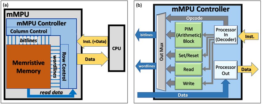
Fig. 2. The mMPU architecture. (a) The interfaces between the mMPU controller, the memory and the CPU. (b) A block diagram of
the mMPU controller. The mMPU controller receives instructions from the CPU, optionally including data to be written, and returns
read data to the CPU via the data lines.
1800 memory cells without cell reuse is compacted into less than 400 memory cells with cell reuse. In this paper, we
assume, without loss of generality, that a logic function is mapped into a single row in the memristive crossbar and
cloned to different rows for different data.
2.5 The memristive Memory Processor Unit (mMPU) Architecture
A PIM system requires a controller to manage its operation. In [3], a design of a memristive memory processing
unit (mMPU) controller is presented. Figure 2 depicts the mMPU architecture, as detailed in [3]. Figure 2(a) describes
the interfaces between the mMPU controller, the memory, and the CPU. The CPU sends instructions to the mMPU
controller, optionally including data to be written to memory. The mMPU processes each instruction and converts it
into one or more memory commands. For each command, the mMPU determines the voltages applied on the wordlines
and bitlines of the memristive memory arrays so that the command will be executed. Figure 2(b) depicts the internal
structure of the mMPU controller. The instruction is interpreted by the decoder and then further processed by one
of the green processing blocks according to the instruction type. The set of mMPU instruction types consists of the
traditional memory instruction types: Load, Store, Set/Reset, and a new family of instructions: PIM instructions. Load
and store instructions are processed in the read and write blocks, respectively. Initialization instructions are processed
in the Set/Reset block. PIM instructions are processed in the PIM ("arithmetic") block. The PIM block breaks each PIM
instruction into a sequence of micro-instructions, and executes this sequence in consecutive clock cycles, as described in
abstractPIM [11]. The micro-instructions supported by the target mMPU controller can be easily adapted and modified
according to the PIM technology in use, e.g., MAGIC NOR and IMPLY. Load instructions return data to the CPU through
the controller via the data lines.
For PIM-relevant workloads, the overhead of the mMPU controller on the latency, power, and energy of the system
is rather low. This is due to the fact that each PIM instruction operates on many data elements in parallel. Thus, the
controller/instruction overhead is negligible relative to the latency, power, and energy cost of the data being processed
within the memristive memory and the data transfer between memory and CPU [39].
Manuscript submitted to ACM6 Ronen, et al.
Fig. 3. Data size reduction illustration. Blue squares: data to be transferred, white: saved data transfer, yellow: bit vector of selected
records to transfer.
3 PIM USE CASES AND COMPUTATION PRINCIPLES
After presenting the motivation for PIM in the previous section, in this section, we describe potential use cases of PIM.
We start with a high-level estimate of the potential benefits of reduced data transfer. Later, we define some computation
principles, and using them, we assess the performance cost of PIM computing.
3.1 PIM Use Cases and Data Transfer Reduction
As stated in Section 2, the benefit of PIM comes mainly from the reduction in the amount of the data transferred
between the memory and the CPU. If the saved time and energy due to the data transfer reduction is higher than the
added cost of PIM processing, then PIM is beneficial. In this sub-section, we list PIM use cases that reduce data transfer
and quantify this reduction.
For illustration, assume our data reflect a structured database in the memory that consists of records, where
each record is mapped into a single row in the memory. Each record consists of fields of varying data types. A certain
compute task reads certain fields of each record, with an overall size of bits, and writes back (potentially zero) bits
as the output. Define = + as the total number of accessed bits per record. Traditional CPU-based computation
consists of transferring × bits from memory to the CPU, performing the needed computations, and writing back
× bits to the memory. In total, these computations require the transfer of × bits between the memory and
the CPU. By performing all or part of the computations in memory, the total amount of data transfer can be reduced.
This reduction is achieved by either reducing (or eliminating) the bits transferred per record (” ”), and/or by
reducing the number of transferred records (” ”).
Several potential use cases follow, all of which differ in the way a task is split between PIM and CPU. In all cases, we
assume that all records are appropriately aligned in the memory, so that PIM can perform the basic computations on all
records concurrently (handling unaligned data is discussed later in Section 3.2). Figure 3 illustrates these use cases.
• CPU Pure. This is the baseline use case. No PIM is performed. All input and output data are transferred to the
CPU and back. The amount of data transferred is × bits.
• PIM Pure. In this extreme case, the entire computation is done in memory and no data is transferred. This kind
of computation is done, for example, as a pre-processing stage in anticipation of future queries. See relevant
examples under PIM Compact and PIM filter below.
• PIM Compact. Each record is pre-processed in memory in order to reduce the number of bits to be transferred
to the CPU from each record. For example, each product record in a warehouse database contains 12 monthly
shipment quantity fields. The application only needs the yearly quantity. Summing ("Compacting") these 12
elements into one reduces the amount of data transferred by 11 elements per record. Another example is an
application that does not require the explicit shipping weight values recorded in the database, but just a short
Manuscript submitted to ACMThe Bitlet Model
A Parameterized Analytical Model to Compare PIM and CPU Systems 7
Table 1. PIM Use Cases Data Transfer Reduction
Use Case Records Size Data Transferred Data Transfer Reduction
× 0
0 0 0 ×
1 × 1 × ( − 1 )
1 1 1 × + × 1 −
2 1 1 × ( + 2 ( )) × − 1 × ( + 2 ( ))
1 1 1 × 1 + × ( − 1) − 1 × 1
0 1 1 1 × 1 × − 1
1 1 = ⌈
⌉ 1 1 × 1 × − 1 × 1
/ 1 : overall/selected number of records; / 1 : original/final size of records.
1 / 2 : bit-vector/list of indices; 0 / 1 : all records/per XB
class tag (light, medium, heavy) instead. If the per-record amount of data is reduced from to 1 bits, then the
overall reduction is × ( − 1 ) bits.
• PIM Filter. Each record is processed in memory to reduce the number of records transferred to the CPU. This is
a classical database query case. For example, an application looks for all shipments over $1M. Instead of passing
all records to the CPU and checking the condition in the CPU, the check is done in memory and only the records
that pass the check ("Filtering") are transferred. If only 1 out of records of size are selected, then the overall
data transfer is reduced by ( − 1 ) × bits. Looking deeper, we need to take two more factors into account:
(1) When the PIM does the filtering, the location of the selected records should also be transferred to the CPU,
and the cost of transferring this information should be accounted for. Transferring the location can be done
by either ( 1 ) passing a bit vector ( bits) or by ( 2 ) passing a list of indices of the selected records
( 1 × 2 ( ) bits). The amount of the total data to be transferred is therefore ( × 1, 1 × 2 ( )). For
simplicity, in this paper, we assume passing a bit vector ( 1 ). The overall cost of transferring both the data
and the bit vector is 1 × + . The amount of saved data transfer relative to CPU Pure is × 1 − bits.
(2) When filtering is done on the CPU only, data may be transferred twice. First, only a subset of the fields (the
size of which is 1 ) that are needed for the selection process are transferred, and only then, the selected records
or a different subset of the records. In this CPU Pure case, the amount of transferred data is × 1 + 1 × .
• PIM Hybrid. This use case is a simple combination of applying both PIM Compact and PIM filter. The amount
of data transferred depends on the method we use to pass the list of selected records, denoted above as 1 or
2 . For example, when using 1 , the transferred data consists of 1 records of size 1 and a bit-vector
of size bits. That is 1 × 1 + .
• PIM Reduction. The reduction operator "reduces the elements of a vector into a single result" 3 , e.g., computes the
sum, or the minimum, or the maximum of a certain field in all records in the database. The size of the result may
be equal to or larger than the original element size (e.g., summing a million of 8-bits arbitrary numbers requires
28 bits). "Textbook" reduction, referred to later as 0 , replaces elements of size with a single element
of size 1 ( 1 ≥ ), thus eliminating data transfer almost completely. A practical implementation, referred to later
as 1 , performs the reduction on each memory array (XB) separately and passes all interim reduction
results to the CPU for final reduction. In this case, the amount of transferred data is the product of the number of
memory arrays used by the element size, i.e., ⌈
⌉ × 1 , where is the number of records (rows) in a single XB.
3 https://en.wikipedia.org/wiki/Reduction_Operator
Manuscript submitted to ACM8 Ronen, et al. 10000 Operational Complexity [# Cycles] 2 13W -14W (MULTIPLY full precision) 8000 2 6.5W -7.5W (MULTIPLY low precision) 6000 4000 2000 0 200 400 600 800 1000 Operation sizes [# Data Bits] Fig. 4. PIM operation complexity in cycles for different types of operations and data sizes. Table 1 summarizes all use cases along with the amount of transferred and saved data. In this table, and 1 reflect the overall and selected number of the transferred records. and 1 reflect the original and final size of the transferred records. 3.2 PIM Computation Principles Stateful logic-based PIM (or just throughout this paper) computation provides very high parallelism. Assuming the structured database example above (Section 3.1), where each record is mapped into a single memory row, PIM can generate only a single bit result per record per memory cycle (e.g., a single NOR, IMPLY, AND, based on the PIM technology). Thus, the sequence needed to carry out a certain computation may be rather long. Nevertheless, PIM can process many properly aligned records in parallel, computing one full column or full row per XB per cycle4 . Proper alignment means that all the input cells and the output cell of all records occupy the same column in all participating memory rows (records), or, inversely, the input cells and the output cell occupy the same rows in all participating columns. PIM can perform the same operation on many independent rows, and many XBs, simultaneously. However, performing operations involving computations between rows (e.g., shift or reduction) or in-row copy of an element with a different alignment in each row, has limited parallelism. Such copies can be done in parallel among XBs, but within a XB, are performed mostly serially. When the data in a XB are aligned, operations can be done in parallel (as demonstrated in Figures 1(b) and 1(c) for row-aligned and column-aligned operations, respectively). However, operations on unaligned data cannot be done concurrently, as further elaborated in Section 3.2. To quantify PIM performance, we first separate the computation task into two steps: Operation and Placement and Alignment. Below, we assess the complexity of each of these steps. For simplicity, we assume computations done on rows and memory arrays, i.e., = × . Operation Complexity ( ). As described in Section 2.3, PIM computations are carried out as a series of basic operations, applied to the memory cells of a row inside a memristive memory array. While each row is processed bit-by-bit, the effective throughput of PIM is increased by the inherent parallelism achieved by simultaneous processing of multiple rows inside a memory array and multiple memory arrays in the system memory. We assume the same computations (i.e., individual operations) applied to a row are also applied in parallel in every cycle across all the rows ( ) of a memory array. 4 The maximum size of a memory column or row may be limited in a specific PIM technology due to e.g., wire delays and write driver limitations. Manuscript submitted to ACM
The Bitlet Model
A Parameterized Analytical Model to Compare PIM and CPU Systems 9

Fig. 5. Horizontal Copies ( ) and Vertical Copies ( ) using PIM. HCOPY: all elements move together, bit per cycle
(case e). VCOPY: all bits move together, element per cycle (case c). Applied together in case g.

 We define Operation Complexity ( ) for a given operation type and data size, as the number of cycles required
to process the corresponding data. Figure 4 shows how the input data length ( ) affects the computing cycles for
PIM-based processing. The figure shows that this number is affected by both the data size, as well as operation types
(different operations follow a different curve on the graph). In many cases, is linear with the data size, for example,
in a MAGIC NOR-based PIM, -bit AND requires 3 cycles (e.g., for =16 bits, AND takes 16x3 = 48 cycles), while
ADD requires 9 cycles5 . Some operations, however, are not linear, e.g., full precision MULTIPLY × → 2 bits
requires 13 2 − 14 cycles [15] or approximately 12.5 2 cycles, while low precision MULTIPLY × → bits
requires about half the number of cycles, or approximately 6.25 2 cycles. The specific Operation Complexity behavior
depends on the PIM technology, but the principles are similar.
 Placement and Alignment Complexity ( ). PIM imposes certain constraints on data alignment and place-
ment [38]. To align the data for subsequent row-parallel operations, a series of data alignment and placement steps,
consisting of copying data from one place to another, may be needed. The number of cycles needed to perform these
additional copy steps is captured by the placement and alignment complexity parameter, denoted as . Currently,
for simplicity, we consider only the cost of intra-XB data copying, we ignore the cost of inter-XB data copying, and we
assume that multiple memory arrays continue to operate in parallel and independently. Refining the model to account
for inter-XB data copying will be considered in the future (see Section 6.5).
 The PAC cycles required to copy the data in a memory array to the desired locations can be broken down into a series
of horizontal row-parallel copies ( ), and vertical column-parallel copies ( ). Figure 5 shows examples
of VCOPY and HCOPY operations involving copying a single element (Figures 5(a), 5(b), 5(d)) and multiple elements
(Figures 5(c), 5(e), 5(f), 5(g)). HCOPYs and VCOPYs are symmetric operations: HCOPY can copy an entire memory
column (or part of it) in parallel, while VCOPY can copy an entire memory row (or part of it) in parallel. Figure 5(g)
depicts the case of copying column-aligned elements, each -bit wide (in green, =2, =5), into different rows to
be placed in the same rows as other column aligned elements (in orange). First, HCOPYs are performed in a bit-serial,
5 ADD can be improved to 7 cycles using four-input NOR gates instead of two-input NOR gates.
 Manuscript submitted to ACM
10 Ronen, et al.

element-parallel, manner (copying elements from green to brown). In the first HCOPY cycle, all the first bits of all
involved elements are copied in parallel. Then, in the second cycle, all the second bits of all involved elements are
copied in parallel. This goes on for cycles until all bits in all elements are copied. Next, VCOPYs are performed
in an element-serial, bit-parallel manner (copying from brown to green). In the first VCOPY cycle, all the bits of the
first selected element are copied, in parallel, to the target row. Then, in the second cycle, all the bits of the second
selected element are copied, in parallel. This goes on for cycles until all elements are copied.
 When the involved data elements across different rows are not aligned, separate HCOPYs are performed individually
for each data element, thus requiring additional cycles. A VCOPY for a given data element, on the other hand, can be
done in parallel on all the bits in the element, which are in the same row. However, each row within a XB has to be
vertically copied separately, in a serial manner.
 The number of cycles it takes to perform a single bit copy (either HCOPY or VCOPY) depends on the PIM technology
used. For example, MAGIC OR-based PIM technology ( [18]) supports logic OR as a basic operation, allowing a 1-cycle
bit copy (see Figure 5(a), 5(c), 5(d), and 5(e)). PIM Technologies that do not support a 1-cycle bit copy (e.g., MAGIC
NOR-based PIM technology), have to execute two consecutive NOT operations that take two cycles to copy a single bit
(Figure 5(b)). However, copying a single bit using a sequence of a HCOPY operation followed by a VCOPY operation
can be implemented as two consecutive OR or NOT operations that take two cycles regardless of the PIM technology
used (Figure 5(f) and 5(g)).
 We define Computation complexity ( ) as the number of cycles required to fully process the corresponding data.
 equals the sum of and .
 Below are examples of PIM cycles. We use the terms Gathered and Scattered to refer to the original layout of the
elements to be aligned. Gathered means that all input locations are fully aligned among themselves, but not with their
destination, while Scattered means that input locations are not aligned among themselves.
 • Parallel aligned operation. Adding two vectors, and , into vector , where , and are in row . The
 size of each element is -bits. A MAGIC NOR-based full adder operation takes (= 9) cycles. Adding two -bit
 elements in a single row takes = × cycles. At the same cycles, one can add either one element or
 millions of elements. Since there are no vertical or horizontal copies, the equals the . The above-mentioned
 PIM Compact, PIM Filter, and PIM Hybrid use cases are usually implemented as parallel aligned operations.
 • Gathered placement and alignment copies. Assume we want to perform a shifted vector copy, i.e., copying
 vector into vector such that −1 ← .6 The size of each element is -bit. With stateful logic, the naive
 way of making such a copy for a single element is by a sequence of operations followed by
 operations. For a given single element in a row , first, copy all bits of in parallel, so ← , then, copy
 −1 ← . Copying -bits in a single row takes cycles. As in the above parallel aligned case, in the same
 cycles, one can copy either one element or many elements. However, in this case, we also need to copy the result
 elements from one row to the adjacent one above. Copying -bits between two rows takes a single cycle, as all
 bits can be copied from one row to another in parallel. But, copying all rows is a serial operation, as it must be
 done separately for each row in the XB. Hence, if the memory array contains rows, the entire copy task will
 take = ( + ) cycles. Still, these operations can be done in parallel on all the XBs in the system. Hence,
 copying all elements can be completed in the same ( + ) cycles.

6 We ignore the elements of that are last in each XB.
Manuscript submitted to ACM
The Bitlet Model
A Parameterized Analytical Model to Compare PIM and CPU Systems 11

 • Gathered unaligned operation. The time to perform a combination of the above two operations, e.g., −1 ←
 + , is the sum of both computations, that is = ( + + ) cycles.
 • Scattered placement and alignment. We want to gather unaligned -bit elements into a row-aligned
 vector , that is, all elements occupy the same columns. Assume the worst case where all elements have to be
 horizontally and vertically copied to reach their desired location, as described above for Gathered placement and
 alignment. To accomplish this, we need to do horizontal 1-bit copies and one parallel -bit copy for each
 element, totaling overall = ( + 1) × cycles.
 • Scattered unaligned operation. Perform a Scattered placement and alignment followed by a parallel aligned
 operation, takes the sum of both computations, that is, = ( + ( + 1) × ) cycles.
 • Reduction. We look at a classical reduction where the reduction operation is both commutative and associative
 (e.g., a sum, a minimum, or a maximum of a vector). For example, we want to sum a vector where each element,
 Í
 as well as the final sum, are of size , i.e., = =1 . The idea is to first reduce all elements in each XB into a
 single value separately, but in parallel, and then perform the reduction on all interim results. There are several
 ways to perform a reduction, the efficiency of which depends on the number of elements and the actual operation.
 We use the tree-like reduction7 , which is a phased process, in which at the beginning of each phase, we start with
 elements ( = , the number of rows, in the first phase), pair them into /2 groups, perform all /2 additions,
 and start a new phase with the /2-generated numbers. For elements, we need ℎ = ⌈log2 ( )⌉ phases. Each
 phase consists of one parallel (horizontal) copy of bits, followed by /2 serial (vertical) copies, and ending
 with one parallel operation (in our case, -bit add). The total number of vertical copies is − 1. Overall, the full
 reduction of a single XB in all phases takes = ( ℎ × ( + ) + ( − 1)) cycles. The reduction is done on all
 involved XBs in parallel, producing a single result per XB. Later, all per XB interim results are copied into fewer
 log ( )
 XBs and the process continues recursively over log2 ( ) steps. Copying all interim results into fewer XBs and
 2
 using PIM on a smaller number of XBs is inefficient as it involves serial inter-XB copies and low-parallel PIM
 computations. Therefore, for higher efficiency, after the first reduction step is done using PIM, all interim results
 are passed to the CPU for the final reduction, denoted as 1 in Section 3.

 Table 2. PIM Computation Cycles for Aligned and Unaligned Computations
 Operate HCOPY VCOPY
 Computation type Row Row Row Total Approximation
 Parallel Parallel Serial
 Parallel Operation - -
 Gathered Placement & Alignment - +
 Gathered Unaligned Operation + + +
 Scattered Placement & Alignment - × ( + 1) × ×
 Scattered Unaligned Operation × + ( + 1) × + ×
 1 ℎ × ℎ × −1 ℎ×( + )+( −1) ℎ × +
 : Operation Complexity, : Width of element, : Number of rows, ℎ: Number of reduction phases.

 Table 2 summarizes the computation complexity in cycles of various PIM computation types (ignoring inter-XB
copies, as mentioned above). Usually, ≫ and ≫ , so ± is approximately , and ± 1 and ± are
approximately . The last column in the table reflects this approximation. The approximation column hints to where
7 https://en.wikipedia.org/wiki/Graph_reduction

 Manuscript submitted to ACM
12 Ronen, et al.

most cycles go, depending on , , and . Parallel operations depend on only and are independent of , the
number of elements (rows). When placement and alignment take place, there is a serial part that depends on and is a
potential cause for computation slowdown.

4 PIM AND CPU PERFORMANCE
In the previous section, the PIM use cases and computation complexity were introduced. In this section, we devise the
actual performance equations of PIM, CPU, and combined PIM+CPU systems.

4.1 PIM Throughput
 represents the time it takes to perform a certain computation, similar to the latency of an instruction in a computing
system. However, due to the varying parallelism within the PIM system, does not directly reflect the PIM system
performance. To evaluate the performance of a PIM system, we need to find its system throughput, which is defined as
the number of computations performed within a time unit. Common examples are Operations Per Second (OPS) or
Giga Operations per Second (GOPS). For a PIM Pure case, when completing computations takes time, the PIM
throughput is:

 = . (1)

 To determine , we obtain the PIM and multiply it by the PIM cycle time ( )8 . depends on the specific
PIM technology used. To compute , we use the equations in Table 2. The number of computations is the total
number of elements participating in the process. When single-row based computing is used, this number is the number
of all participating rows, which is the product of the number of rows within a XB with the number of XBs, that is,
 = × . The PIM throughput is therefore
 × .
 = × (2)

 For example, consider the Gathered unaligned operation case for computing shifted vector-add, −1 ← + .
Assuming = 9 cycles (1-bit add), element size = 16 bits, = 1024 rows, and = 1024 memory arrays, then
 = 1 elements. = 9×16 = 144 cycles. The number of cycles to compute elements also equals the time to compute
 = 1024×1024 = 1598
 elements and is = + or 144 + 512 = 656 cycles. The PIM throughput per cycle is 656
computations per cycle. The throughput is 1598
 computations per time unit. We can derive the throughput per second
for a specific cycle time. For example, for a of 10ns, the PIM throughput is 1598
 10−8
 = 159.8 × 10⁹ OPS ≈ 160 GOPS.
 In the following sections, we explain the CPU Pure performance and throughput and delve deeper into the overall
throughput computation when both PIM and CPU participate in a computation.

4.2 CPU Computation and Throughput
Performing computation on the CPU involves moving data between the memory and the CPU (Data Transfer), and
performing the actual computations (e.g., ALU Operations) within the CPU core (CPU Core). Usually, on the CPU side,
Data Transfer and CPU Core Operations can overlap, so the overall CPU throughput is the minimum between
the data transfer throughput and the CPU Core Throughput.
 Using PIM to accelerate a workload is only justified when the workload performance bottleneck is the data transfer
between the memory and the CPU, rather than the CPU core operation. In such workloads, the data-set cannot fit in
8 We assume that the controller impact on the overall PIM latency is negligible, as explained in Section 2.5.
Manuscript submitted to ACM
The Bitlet Model
A Parameterized Analytical Model to Compare PIM and CPU Systems 13

the cache as the data-set size is much larger than the CPU cache hierarchy size. Cases where the CPU core operation,
rather than the data transfer, is the bottleneck, are not considered PIM-relevant. In PIM-relevant workloads, the overall
CPU throughput is dominated by the data transfer throughput.
 The data transfer throughput depends on the memory to CPU bandwidth and the amount of data transferred per
computation. We define as the memory to CPU bandwidth in bits per second (bps), and ( ) as the
number of bits transferred for each computation. That is:
 .
 = (3)

 We demonstrate the data transfer throughput using, again, the shifted 16-bit vector-add example. In Table 3, we
present three interesting cases, differing in their size. (a) CPU Pure. The two inputs and the output are transferred
between the memory and the CPU ( = 48). (b) Inputs only. Same as CPU Pure, except that only the inputs are
transferred to the CPU; no output result is written back to memory ( = 32). (c) Compaction. Where PIM performs
the add operation and passes only the output data to the CPU for further processing ( = 16). We use the same
data bus bandwidth, = 1000 GOPS, for all three cases. Note that the data transfer throughput depends only on
the data sizes, it is independent of the operation type. The throughput numbers in the table reflect any binary 16-bit
operation, either simple as OR or complex as divide. The table hints at the potential gain that PIM opens by reducing
the amount of data transfer between the memory and CPU. If PIM throughput is sufficiently high, the data transfer
reduction may compensate for the additional PIM computations and the combined PIM+CPU system throughput may
exceed the throughput of a system using the CPU only with PIM.
 Special care must be taken when determining DIO for the PIM Filter and PIM Reduction cases since only a subset
of the records are transferred to the CPU. Note that the DIO parameter reflects the number of data bits transferred
per accomplished computation, even though the data for some computations were not eventually transferred. In these
cases, the DIO should be set as the total number of transferred data bits divided by the number of computations done
in the system. For example, assume a filter, where we process records of size , and pass only = × of them
 ( × × )+
( < 1). The DIO, in case we use a bit-vector to identify chosen records, is = ( × ) + 1. e.g., if = 200 and
 = 1%, DIO is 200 × 0.01 + 1 = 2 + 1 = 3 bits. That is, the amount of data transfer per computation went from 200 to 3
bits per computation, i.e., 67× reduction. The data transfer throughput for the filter case is presented in Table 3.

 Table 3. Data Transfer Throughput
 Bandwidth (BW) DataIO (DIO) Data Transfer Throughput ( )
 Computation type
 [Gbps] [bits] [GOPS]
 CPU Pure 1000 48 20.8
 Inputs Only 1000 32 31.3
 Compaction 1000 16 62.5
 Filter (200 bit, 1%) 1000 3 333.3

4.3 Combined PIM and CPU Throughput
In a combined PIM and CPU system, achieving peak PIM throughput requires operating all XBs in parallel, thus
preventing overlapping PIM computations with data transfer9 . In such a system, completing computations takes

9 Overlapping PIM computation and data transfer can be made possible in a banked PIM system. See Pipelined PIM and CPU in Section 6.5.
 Manuscript submitted to ACM
14 Ronen, et al.

 PIM time and data transfer time, and the combined throughput is, by definition:

 =
 + . (4)

 Fortunately, computing the combined throughput does not require knowing the values of and
 . can be computed using the throughput values of its components, and , as follows:

 = 1 1 (5)
 + =
 +
 = 1
 + 1
 .

 Since the PIM and CPU operations do not overlap, the combined throughput is always lower than the throughput of
each component for the pure cases with the same parameters. For example, in the Gathered unaligned operation case
above, when computing a 16-bit shifted vector-add, i.e., −1 ← + , we do the vector-add in PIM, and transfer the
16-bit result vector to the CPU (for additional processing). We have already shown that, for the parameters we use,
the PIM Throughput is = 160 GOPS, and the data transfer throughput is = 62.5 GOPS. Using Eq. (5),
the combined throughput = 1 = 44.9 × 109 = 44.9 GOPS, which is indeed lower than 160 and
 1 1
 +
 160×109 62.5×10⁹
62.5 GOPS. However, this combined throughput is higher than that of the CPU Pure throughput using higher =32
or =48 (31.3 or 20.8 GOPS) presented in the previous subsection. Of course, these results depend on the specific
parameters used here. A comprehensive analysis of the performance sensitivity is described in Section 6.2.

5 POWER AND ENERGY
When evaluating the power and energy aspects of a system, we examine two factors:

 • Energy per computation. The energy needed to accomplish a single computation. This energy is determined
 by the amount of work to be done (e.g., number of basic operations) and the energy per operation. Different
 algorithms may produce different operation sequences thus affecting the amount of work to be done. Physical
 characteristics of the system affect the energy per operation. Energy per Computation is a measure of system
 efficiency. A system configuration that consumes less energy per a given computation is considered more efficient.
 For convenience, we generally use Energy Per Giga Computations. Energy is measured in Joules.
 • Power. The power consumed while performing a computation. The maximum allowed power is usually deter-
 mined by physical constraints like power supply and thermal restrictions, and may limit system performance. It
 is worth noting that the high parallel computation of PIM causes the memory system to consume much more
 power when in PIM mode than when in standard memory load/store mode. Power is measured in Watts (Joules
 per second).

 In this section, we evaluate the PIM, the CPU, and the combined system power and energy per computation and how
it may impact system performance. For the sake of this coarse-grained analysis, we consider dynamic power only and
ignore power management and dynamic voltage scaling.

5.1 PIM Power and Energy
Most power models target a specific design. The below approach is more general and resembles the one used for
floating-point add/multiply power estimation in FloatPIM [20]. In this approach, every PIM operation consumes energy.
For simplicity, we assume that in every PIM cycle, the switching of a single cell consumes a fixed energy . This
is the average amount of energy consumed by each participating bit in each XB, and accounts for both the memristor
access as well as other overheads such as the energy consumed by the wires and the peripheral circuitry connected to
Manuscript submitted to ACM
The Bitlet Model
A Parameterized Analytical Model to Compare PIM and CPU Systems 15

the specific bitline/wordline10 . The PIM energy per computation is the product of by the number of
cycles . The PIM power is the product of the energy per computation by the PIM throughput
(see Section 4.1).

 = × , (6)
 × = × × .
 = × = ( × ) × × (7)

5.2 CPU Power and Energy
Here we compute the CPU energy per computation and the power . As in the performance model, we
ignore the actual CPU Core operations and consider only the data transfer power and energy. Assume that transferring
a single bit of data consumes . Hence, the CPU energy per computation is the product of by
the number of bits per computation . The CPU power is simply the product of the energy per computation
 with the CPU Throughput . When the memory to CPU bus is not idle, the CPU power is equal to
the product of the energy per bit with the number of bits per second, which is the memory to CPU bandwidth
 .

 = × , (8)
 =
 = × = × × × . (9)

 If the bus is busy only part of the time, the CPU power should be multiplied by the relative time the bus is
busy, that is, the bus duty cycle,

5.3 Combined PIM and CPU Power and Energy
When a task is split between PIM and CPU, we treat them as if part of each computation is partly done on the PIM and
partly on the CPU (see Section 4.3). The combined energy per computation is the sum of the PIM energy
per computation and the CPU energy per computation . The overall system power is the product of
the combined energy per computation and the combined system throughput:

 = + = +

 , (10)

 = × = ( +
 ) × . (11)

 Since PIM and CPU computations do not overlap, their duty cycle is less than 100%. Therefore, the PIM power in the
combined PIM+CPU system is lower than the maximum PIM Power in a Pure PIM configuration. Similarly, the CPU
Power in the combined PIM+CPU system is lower than the maximum CPU Power.
 In order to compare energy per computation between different configurations, we use the relevant values,
computed by dividing the power of the relevant configuration by its throughput. That is:

 = ; =

 ; =

 . (12)

 The following example summarizes the entire power and energy story. Assume, again, the above shifted vector-
add example using the same PIM and CPU parameters. In addition, we use = 0.1pJ [26] and =
15pJ [29]. The PIM Pure throughput is 160 GOPS (see Section 4.1) and the PIM Pure power is = × × =

10 We assume that the controller impact on the overall PIM power and energy is negligible, as explained in Section 2.5.
 Manuscript submitted to ACM
16 Ronen, et al.

0.1∗10−12 ×1024×1024 = 10.5W. The CPU Pure throughput (using = 1000 Gpbs) is 20.8 (or 62.5) GOPS for 48 (or 16) bit
 10−8
DIO (see Section 4.2). The CPU Pure Power is = × =15*10−12 × 1012 = 15W. A combined PIM+CPU
system will exhibit throughput of = 44.9 GOPS and power = ( +

 ) × =
 10.5 15 9
( 160×109 + 62.5×10⁹ ) × (44.9 × 10 ) = 13.7W.
 Again, these results depend on the specific parameters in use. However, they demonstrate a case where, with PIM,
not only the system throughput went up, but, at the same time, the system power decreased. When execution time and
 15
power consumption go down, energy goes down as well. In our example, = 20.8×10 0.72
 9 = 109 J/OP = 0.72 J/GOP,
 13.7 = 0.31 J/OP = 0.31 J/GOP.
and = 44.9×10⁹ 109

5.4 Power-Constrained Operation
Occasionally, a system, or its components, may be power-constrained. For example, using too many XBs in parallel, or
fully utilizing the memory bus may exceed the maximum allowed system or component thermal design power 11 ( ).
For example, the PIM power must never exceed . When a system or a component exceeds its , it has
to be slowed down to reduce its throughput and hence, its power consumption. For example, a PIM system throughput
can be reduced by activating fewer XBs or rows in each cycle, increasing the cycle time, or a combination of both. CPU
power can be reduced by forcing idle time on the memory bus to limit its bandwidth (i.e., "throttling").

6 THE BITLET MODEL - PUTTING IT ALL TOGETHER
So far, we have established the main principles of the PIM and CPU performance. In this section, we first present
the Bitlet model itself, basically summarizing the relevant parameters and equations to compute the PIM, CPU, and
combined performance in terms of throughput. Then, we demonstrate the application of the model to evaluate the
potential benefit of PIM for various use cases. We conclude with a sensitivity analysis studying the interplay and impact
of the various parameters on the PIM and CPU performance and power.

6.1 The Bitlet Model Implementation
The Bitlet model consists of ten parameters and nine equations that define the throughput, power, and energy of the
different model configurations. Table 4 summarizes all Bitlet model parameters. Table 5 lists all nine Bitlet equations.
 PIM performance is captured by six parameters: , , , , and . Note that and are just
auxiliary parameters used to compute . CPU performance is captured by two parameters: and . PIM and
CPU energy are captured by the and the parameters. For conceptual clarity and to aid our analysis, we
designate three parameter types: technological, architectural, and algorithmic. Typical values or ranges for the different
parameters are also listed in Table 4. The table contains references for the typical values of the technological parameters
 , , and , which are occasionally deemed controversial. The model itself is very flexible, it accepts
a wide range of values for all the parameters. These values do not even need to be implementable and can differ
from the parameters’ typical values or ranges. This flexibility allows limit-studies by modeling systems using extreme
configurations.
 The nine Bitlet model equations determine the PIM, CPU and the combined performance ( , , ),
power ( , , ), and energy per computation ( , , ).

11 https://en.wikipedia.org/wiki/Thermal_design_power

Manuscript submitted to ACM
The Bitlet Model
A Parameterized Analytical Model to Compare PIM and CPU Systems 17

 Table 4. Bitlet Model Parameters.
 Parameter name Notation Typical Value(s) Type
 PIM operation complexity 1 - 64k cycles Algorithmic
 PIM placement and alignment complexity 0 - 64k cycles Algorithmic
 PIM computational complexity = + 1 - 64k cycles Algorithmic
 PIM cycle time 10 ns [26] Technological
 PIM array dimensions (rows × columns) × 16x16 - 1024x1024 Technological
 PIM array count 1 - 64k Architectural
 PIM energy for operation ( =1) per bit 0.1pJ [26] Technological
 CPU memory bandwidth 0.1 - 16 Tbps Architectural
 CPU data in-out bits 1 - 256 bits Algorithmic
 CPU energy per bit transfer 15pJ [29] Technological

 Table 5. Bitlet model Equations

 Entity Equation Units

 PIM Throughput ×
 = × GOPS

 CPU Throughput
 = GOPS

 Combined Throughput = 1 GOPS
 1
 + 1

 PIM Power = × × Watts

 CPU Power = × Watts

 Combined Power = ( +
 ) × Watts

 PIM Energy per Computation = J/GOP

 CPU Energy per Computation = J/GOP

 Combined Energy per Computation = J/GOP

6.2 Applying The Bitlet Model
The core Bitlet model is implemented as a straightforward Excel spreadsheet12 . All parameters are inserted by the user
and the equations are automatically computed. Figure 6 is a snapshot of a portion of the Bitlet Excel spreadsheet that
reflects several selected configurations.
 Few general notes:
 • The spreadsheet can include many configurations, one per column, simultaneously, allowing a wide view of
 potential options to ease comparison.
 • For convenience, in each column, the model computes the three related PIM Pure (PIM), CPU Pure (CPU), and
 the Combined configurations. To support this, the two DIO parameters are needed; one, , for the CPU
 Pure system, and one (usually lower), , for the combined PIM+CPU system. See rows 13-14 in the
 spreadsheet.
 • Determining the , , and parameters needs special attention. Sections 3.2 and 4.2 detail how to
 determine these parameters.
12 The spreadsheet is available at https://asic2.group/tools/architecture-tools/
 Manuscript submitted to ACM
18 Ronen, et al.

 Fig. 6. Throughput and Power comparison of CPU Pure vs. combined PIM+CPU system.

 • Fonts and background are colored based on the system they represent: blue for PIM, green for CPU, and red for
 combined PIM+CPU system.
 • Bold parameter cells with a light background mark items highlighted in the following discussions and are not
 inherent to the model.
 Following is an in-depth dive into the various selected configurations.
 Compaction. Cases 1a-1f (columns E-O) describe simple parallel aligned operations. In all these cases, the PIM
performs a 16-bit binary computation in order to reduce data transfer between the memory and the CPU from 48 bits
to 16 bits. The various cases differ in the operation type (OR/ADD/MULTIPLY, columns E-G), the PIM array count
(1024/16384 XBs), and the CPU memory bandwidth (1000/16000 Gpbs) see cases 1b, 1d-1f, rows 4, 10 and 12. Note that
in row 3, "pim" means a small PIM system (1024 XBs) while "PIM" mean a large PIM system (16384 XBs). Same holds for
"cpu" (1Tbs) and "CPU" (16Tbs). In each configuration, we are primarily interested in the difference between the CPU
and the combined PIM+CPU system results. Several observations:
 • A lower (row 5) yields higher PIM throughput and combined PIM+CPU system throughput. The combined
 PIM+CPU system provides a significant benefit over CPU for OR and ADD operations, yet almost no benefit for
 MULTIPLY.
 • When the combined throughput is close to the throughput of one of its components, increasing the other
 component has limited value (e.g., in case 1d, using more XBs (beyond 1024) has almost no impact on the
 combined throughput (61 GOPS), as the maximum possible throughput with the current bandwidth (1000 Gbps)
 is 62 GOPS).
 • When the throughput goes up, so does the power. Using more XBs or higher bandwidth may require higher
 power than the system . Power consumption of over 200 Watts is likely too high. Such a system has to be
 slowed down by activating fewer XBs, enforcing idle time, etc...
 • A comparison of the PIM throughput and the CPU throughput (row 18 and 20) provides a hint as to how to speed
 up the system. Looking at case 1b (column F), the PIM throughput is 728 GOPS while the CPU throughput is 63
Manuscript submitted to ACM
You can also read