Application Report A New Off-Line LED Lighting Driver Solution with Multi-Transformer LLC Control
←
→
Page content transcription
If your browser does not render page correctly, please read the page content below
A New Off-Line LED Lighting Driver Solution
with Multi-Transformer LLC Control

Application Report

                  Literature Number: SLUA617A
                          September 2011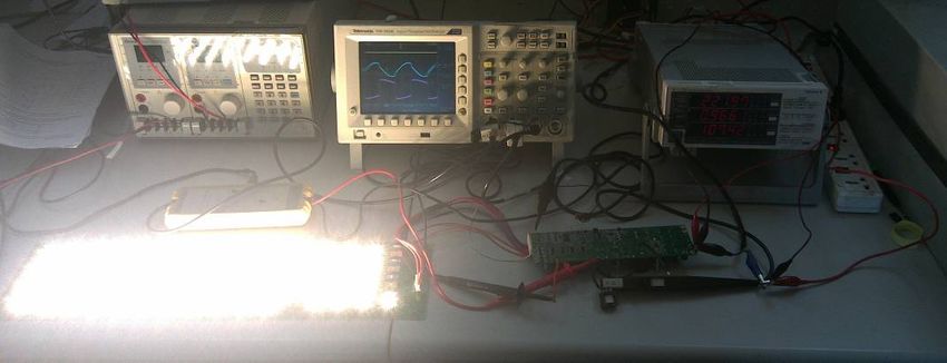
Application Report
                                                                                SLUA617A – September 2011 – Revised September 2011

                         A New Off-line LED Lighting Driver Solution with
                                          Multi-Transformer LLC Control
Pony Ma, Jimmy Liu                                                                                      China Power Reference Design

                                                                   ABSTRACT

         With TI multi-transformer LLC controller UCC25710, this application note introduces a
         new off line LED lighting driver solution. Compared to conventional high wattage (>100W)
         LED lighting driver with AC/DC plus multiple constant current DC/DC converter stages,
         the new topology can have higher efficiency and lower system cost. A 100W LED lighting
         driver reference design PMP4302A using this multi-transformer LLC control is developed.
         This design drives 4 LED strings with 500mA current and 15 LEDs in series for each string.
         The experimental results show the new topology is very suitable for general LED lighting
         applications for both outdoor and commercial applications with PWM or analog dimming.
         Meanwhile, the architecture can also be used for TV LED backlight power providing high
         efficiency and ultra-slim form factor.

                                                                 Contents
1   Introduction .....................................................................................................................................2
2   Proposed Topology.........................................................................................................................3
    2.1 Traditional topology for high wattage off-line LED lighting driver ..............................................3
    2.2 New topology for high wattage off-line LED lighting driver ........................................................4
3   New Multi-transformer LLC controller...........................................................................................5
4   LLC Multi-transformer design ........................................................................................................6
5   100W off-line LED lighting driver design ....................................................................................11
    5.1 Design Specification................................................................................................................12
    5.2 Schematics..............................................................................................................................14
    5.3 Output Current Matching .........................................................................................................16
    5.4 Efficiency .................................................................................................................................18
    5.5 Dimming waveform..................................................................................................................19
    5.6 LLC stage waveforms..............................................................................................................21
    5.7 EMI performance.....................................................................................................................21
6   Conclusion.....................................................................................................................................22
References.............................................................................................................................................22

                                                     Figures
Figure 1.          Traditional high wattage off-line LED lighting driver’s topology...................................3
Figure 2.          Proposed new high wattage off-line LED lighting driver................................................4
Figure 3.          Simplified block diagram for multi-string LLC control UCC25710 ................................6
Figure 4.          Multi-string transformer structures ..................................................................................6
Figure 5.          Simplified architecture for multi-string LLC topology with boost PFC.........................7
Figure 6.          Simplified equivalent network for LLC topology.............................................................8
Figure 7.          DC gain curve for LLC topology .....................................................................................10
Figure 8.          Demo board for PMP4302A reference design ...............................................................12
Figure 9.          PFC stage schematics for PMP4302A ............................................................................14

                                                                                                                                                      1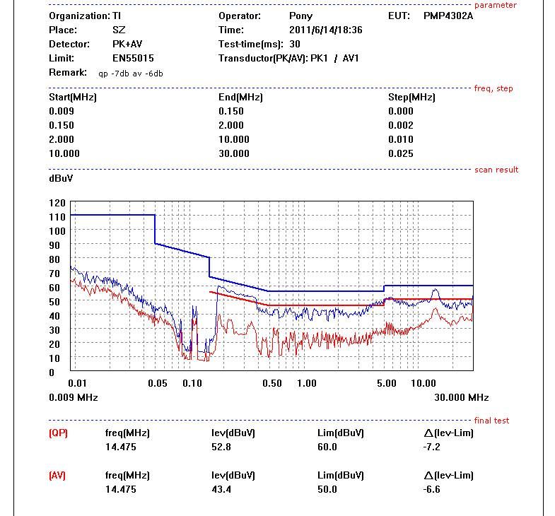
SLUA617A – September 2011 – Revised September 2011

Figure 10.     Multi-string LLC stage schematics of PMP4302A .........................................................15
Figure 11.     Auxiliary Flyback stage schematics of PMP4302A .......................................................16
Figure 12.     Efficiency curve with dimming........................................................................................18
Figure 13.     Operating waveforms during PWM dimming.................................................................20
Figure 14.     LLC stage waveforms at full load ...................................................................................21
Figure 15.     EMI conduction test results.............................................................................................22

                                                  Tables
Table 1.       Electrical Design Specification .......................................................................................13
Table 2.       Output current with input voltage...................................................................................17
Table 3.       Output current with PWM dimming and input voltage..................................................17

1      Introduction
       Nowadays, LED technology has emerged as a promising lighting technology to replace the
       energy-inefficient incandescent lamps and mercury-based fluorescent lamps. Among general
       LED lighting applications, high wattage (>100W) off-line LED lighting shows great energy saving
       and long lifespan compared with conventional lamps, such as high pressure sodium lamps and
       CFL lamps. The target markets for high wattage professional LED lighting are outdoor LED
       street lights and other commercial LED lights.
       To make the same brightness for each LED, a constant current source should be implemented
       for the driving system. Normally, for power ratings more than 65W, LED matrix will consist of
       several LED strings in parallel. And, each string should be controlled by a constant current
       source and each string current should be equal to insure uniform system brightness. In addition,
       the power system should also ensure the input current has the same phase and shape of the
       input AC line voltage. Thus, a PFC circuit is needed to reduce the current harmonics.
       Besides the above mentioned features, efficiency and reliability are very critical for high wattage
       LED lighting. High efficiency is not only the basic requirement for energy saving, but also for the
       power system itself. Because thermal design is always a big issue for LED lighting systems it
       can lead to high ambient temperatures for the power. A high efficiency LED driver will help
       system reliability and thermal performance.
       This application note presents a new multi-transformer LLC converter for high wattage LED
       lighting driver solution. By using the proposed topology, high efficiency and high reliability can be
       achieved with magnetizing balance to drive multiple LED strings. A 100W reference design
       PMP4302A is built to verify the overall performance with a PWM dimming interface.

2   A New Off-line LED Lighting Driver Solution with Multi-Transformer LLC Control
SLUA617A – September 2011 – Revised September 2011
2 Proposed Topology
2.1 Traditional topology for high wattage off-line LED lighting driver
Figure 1 shows a typical high wattage off line LED lighting driver topology. In this structure, the
PFC stage shapes the input current to a sinusoidal wave. The boost topology is the best
candidate for this stage due to its continuous input current and easy configuration. Thus for the
wide range input voltage of 85V~264Vac, the output of PFC stage will be higher than the peak
input voltage. 380VDC to 400VDC bus is normally selected. Because the PFC output voltage is
too high and it is non-isolated, a DC/DC stage with transformer isolation is needed. Normally a
half bridge LLC resonant converter is used because of its high efficiency and good EMI
performance. The DC/DC stage generates the intermediate bus voltage to drive the LED strings.
The output voltage level for this stage is based on the number of LEDs and the next constant-
current control stage; normally it is below 60Vdc in keeping with the standard safety extra low
voltage (SELV). Each LED string will have an individual constant current regulator to regulate
the LED current. For most popular high brightness (HB) LED, the current specification range is
from 350mA to 750mA.
400V
L
Q
r
1
PFC L
EMI Control LLC
m
Control
Q Buck Buck
2
C Control Control
r
Figure 1. Traditional high wattage off-line LED lighting driver topology
Even thought traditional high wattage off-line LED lighting drivers can achieve good performance,
there are some drawbacks:
1. Efficiency. The traditional structure is a three stage topology, which includes PFC, isolated
PWM and non-isolated DC/DC. The most optimized efficiencies for each stage are 97% for
PFC stage, 96% for isolated PWM stage, and 95% for DC/DC stage. So total maximum
efficiency it can achieve is about 88%. Of course, there are some methods to improve the
efficiency further, such as synchronous rectifier control for both isolated PWM and DC/DC
stages, but it is not cost effective.
2. Cost. From the above figure 1, there are multiple DC/DC stages on each LED string, which
will lead to high cost on this stage with multiple controllers, inductors and capacitors.
3. Reliability. Because there are many external components on the traditional LED lighting
topology, which will highly influence the performance.
A New Off-line LED Lighting Driver Solution with Multi-Transformer LLC Control 3SLUA617A – September 2011 – Revised September 2011
4. EMI. Because multiple switching LED drivers will generate additional high frequency
switching noise on the DC/DC stages, and hence affect the measurement results of both
conducted and radiated EMI in the LED lamp. More EMI design effort will be required, for
example RC snubber network at switch node, EMI filter at output stage or synchronizing the
multiple DC/DC controllers.
2.2 New topology for high wattage off-line LED lighting driver
To address these issues of the typical topology, this application note introduces a new topology
using TI’s multi-transformer LLC controller, the UCC25710. Figure 2 shows a block diagram for
this new topology. It includes only two stages, the PFC and the multi-transformer LLC converter.
After PFC stage, there is an isolated half bridge multi-string LLC converter, which makes the
primary windings of transformers electrically connected in series. Based on the theory of
magnetic balance, since the current of primary windings are the same when in series, the output
current for each isolated transformer will have the same current to drive each LED string. And
each transformer can drive two LED strings.
The multi-transformer LLC controller (UCC25710 in this design) is located on the secondary side,
where it senses the sum of LED strings’ current and regulates the sinusoidal ac current that
flows through primary windings by using current loop feedback, which makes a constant current
output for each LED string.
400Vdc
EMI PFC
Input Bridge Control
CS
UV
OV
Ga Gb
PWM
Control
Figure 2. Proposed new high wattage off-line LED lighting driver
The new topology has some key features when compared with the traditional LED lighting driver
topology:
1. High Efficiency. Because it only has two stages, PFC plus multi-transformer LLC, the
estimated total efficiency will be higher than 91%. The efficiency will be highly determined by
the LLC converter design.
4 A New Off-line LED Lighting Driver Solution with Multi-Transformer LLC ControlSLUA617A – September 2011 – Revised September 2011
2. Low cost. Compared with the conventional topology for high wattage LED lighting, the new
topology only includes two stages and fewer controllers, which is cost effective.
3. High system reliability. As we known, reliability of the LED lighting is determined by thermal
management of the LEDs and the electrical drive, fault detection and protection of the
system, as well as electrical component count. Because of the lower component count on
this new topology and good efficiency, the reliability will be greatly improvement.
4. Good EMI performance. Because there are no multiple DC/DC stages on the output, it will
help for EMI performance. Meanwhile, LLC converter is operating with ZVS operation that
can help reduce noise during switching.
5. Dimming compatible. Because the LLC controller is located on the secondary side, the total
current of each string is summed and feedback as a current feedback loop, which can easily
implement PWM dimming or analog dimming.
Unlike the traditional LED lighting topology, the new LED lighting topology will help to reduce
component count, improve efficiency, and help reduce board size.
3 New Multi-transformer LLC controller
The UCC25710 is based on the LLC resonant half bridge topology. The controller feedback loop
is configured to regulate the total current of all LED strings typically with a current sense resistor.
As shown in figure 3, the total current for the LED strings is sensed by R3 at the CS pin and a
current loop error amplifier is designed to maintain a steady state operating voltage point of the
current amplifier during dimming operation. The output of current amplifier, ICOMP, will set the
control voltage to the VCO (Voltage Controlled Oscillator), which incorporates a programmable
minimum and maximum frequency. This is configured to a close current feedback loop for an
LLC topology with LED lighting strings. The optimum ICOMP capacitor C1 is determined based
on the desired LED current and primary current response during dimming.
There are three factors that can control the VCO for LLC control. Firstly, the control voltage to
the VCO is set by ICOMP (current loop error amplifier output) during LED on-times. Secondly,
during start up, the soft start pin SS will control the VCO response until it exceeds ICOMP.
Thirdly, during dimming the rise and fall rates of the VCO input are controlled by the voltage at
the dimming slew rate capacitor C2, DSR pin, while the pedestal of VCO control level will
continue to be controlled by ICOMP.
The DSR capacitor C2 and internal 44μA current control the slew rate of VVCO during dimming off
and on transitions. When turn off, DSR is discharged to ground by a 44μA current sink and when
turn on, DSR is charged to ICOMP voltage by a 44μA source. This will allow potentially audible
electro-mechanically induced noise to be minimized.
The LED dimming input, ILED-ON, controls the LED lighting dimming on and off. In addition, the
falling, or turn-off, edge of a dimming cycle can be delayed, allowing the current loop to maintain
control at low dimming duty-cycles even when the ramp rates have been slowed.
In summary, the UCC25710 device includes all of the functions necessary to implement a total
LED backlight driver including GM current loop error amplifier, VCO, reference regulator, soft
start, dimming duty cycle compensation and protection for OV, UV, current limit, and thermal
shut down. There are additional features to minimize audible noise during dimming and provide
fast LED current rise and fall times.
A New Off-line LED Lighting Driver Solution with Multi-Transformer LLC Control 5SLUA617A – September 2011 – Revised September 2011
In addition to multi-transform LLC topology, UCC25710 is also a good LLC controller for high-
volt single LED string output applications with a dimming interface and reduced audible noise.
VREF
5 VVCO VVCO
LED R1 CREF
RETURN VCLREFCLO, 0.5V
15 VCLREFCHI, 2.8V
R2 Current
Amplifier
+
CS + H VVREF
+
16
GMICOMP Control
R3 510uS Clamp
+ VVREF
17
Dimming Slew IDSRCH
C1 ICOMP Control
ICOMP 44uA
DSR GND ILED-ON’
4K H
14
C2 VVREF L
IDSRDC
VCC delay 44uA
LEDSW 2.4us
6 ILED-ON
Figure 3. Simplified block diagram for multi-string LLC control UCC25710
4 LLC Multi-transformer design
The innovation of multi-transformer to match current simply uses the magnetic balance theory.
As shown in figure 4, the primary windings of multiple transformers are connected in series, in
the ideal case, the same primary side currents result in the same secondary side current if the
transformer turns ratio is the same.
⎧⎪ I p1 = I p 2
⎨ (1)
⎪⎩ I s1 = I s 2 = n × I p1
The transformer is not an ideal component; it also includes magnetizing inductor, due to the
existence of the magnetizing inductor in the transformer, the secondary side current will be
slightly different on the output LED string. Fortunately, the magnetizing current is only a small
portion of the primary side current and the current match is not sensitive to the differences in the
magnetizing current. In order to achieve perfect current matching, it is recommended to increase
the magnetizing inductance Lm for the multi-transformer LLC design.
Ip1
Is1
1:n
Im1
Ip2 Is2
Im2
1:n
Figure 4. Multi-string transformer structures
6 A New Off-line LED Lighting Driver Solution with Multi-Transformer LLC ControlSLUA617A – September 2011 – Revised September 2011
To simplify the solution, the topology uses one transformer to drive two LED strings. In the same
transformer, when the primary ac sinusoidal current is flowing positively, the secondary current
is conducted with the same coupling direction. On the other hand, when the primary sinusoidal
ac current is flowing reversely, the other current loop on the secondary side is conducting during
the switching cycle, as shown in figure 5. The DC blocking capacitor on the output guarantees
the positive current and negative current are the same during each switching cycle.
Figure 5. Simplified architecture for multi-string LLC topology with boost PFC
The design of the multi-transformer LLC transformer is similar to a conventional LLC converter
design. To use the conventional LLC converter design process, the multiple transformers and
reflected loads can be combined into one equivalent transformer load. Once resonant inductor
Ls and magnetizing inductor Lm are determined based on a single transformer; simply divide by
the number of transformers for each transformer specification target. When operation frequency
is equal to the series resonant frequency, input and output voltage for this multi-string LLC
converter can be expressed as:
VDCBUS
VLED = (2)
2 × n × NT
Where, n is the primary to secondary turns ratio; VDCBUS is the input voltage of the LLC
converter, typically it is the output of the PFC boost converter; VLED is the voltage of LED string
and NT is the number of transformer. In the practical design of 100W two string LLC converter,
Input voltage is set at 340 V to 410 V from PFC with nominal point 400 V; The output is equal to
,
50V / 1 A with two transformer in series. So the equivalent turn ratio is n = n × NT = 4 .
Meanwhile, the operating frequency is set at around 120 KHz, which is a little higher than the
resonant frequency to achieve good current matching.
A New Off-line LED Lighting Driver Solution with Multi-Transformer LLC Control 7SLUA617A – September 2011 – Revised September 2011
MOSFET turn-off current should be able to discharge junction caps during the dead-time (500ns);
the following equation should be met to get ZVS operation.
T ⋅ t dead
Lm ≤ (3)
16 ⋅ Ceq
In the design, it uses a simplified method applied to any resonant topology based on the
assumption that input-to-output power transfer is due to the fundamental Fourier Series
components of currents and voltages, which is the commonly know as FHA (First Harmonic
Approximation).
In the below figure 6, the input of the equivalent network is a square waveform with 50% duty
cycle, and the output is also a square waveform with 50% duty cycle, of which amplitudes are
Vin / 2 and nVo respectively.
Figure 6. Simplified equivalent network for LLC topology
Considering the fundamental harmonic element of input and output, the DC gain of input to
output can be expressed as the following equation:
jω L m n 2 R o
nV o jω L m + n 2 R o
=
V in / 2 1 jω L m n 2 R o
+ jω L s +
jω C s jω L m + n 2 R o
nV o 1
=
Vin / 2 2 2 2 2 (4)
⎛ 1 ⎞ ⎛ω2 ⎞ ⎛ 1 ⎞ ⎛ ω2 ⎞
⎜⎜ 2 ⎟⎟ ⎜⎜ 2 − 1 ⎟⎟ + ⎜⎜ ⎟⎟ ⎜⎜ 1 − 2 ⎟⎟
⎝ ω Lm C s ⎝ ωm ⎠ ⎝ ω C s n Ro ωs
2
⎠ ⎠ ⎝ ⎠
Where, ω s is the resonant angle frequency of Ls and Cs in series:
1
ωs = (5)
LsCs
8 A New Off-line LED Lighting Driver Solution with Multi-Transformer LLC ControlSLUA617A – September 2011 – Revised September 2011
ω m is the resonant angle frequency if C s , Ls and Lm in series
1
ωm = (6)
(Lm + Ls )C s
The variables in equation (4) can be replaced by three normalized variables
fn is the normalized frequency to the series resonant frequency of
Ls and C s .
ω
fn = (7)
ωs
Q is the load resistance normalized to the impedance of the resonant inductance at the series
resonant frequency.
n 2 ⋅ Ro
Q= (8)
ω s Ls
h is the factor for magnetizing inductance normalized to resonant inductance.
L
h= m (9)
Ls
Using the equivalent circuit, a normalized DC gain equation is derived as follows:
nV o 1 (10)
M ( fn , h, Q ) = =
V in / 2 1 1 1
(1 + − )2 + Q 2 ⋅ ( − fn )2
2
h fn ⋅ h fn
A plot of this equation, for various Q values, can be seen in figure 7.
A New Off-line LED Lighting Driver Solution with Multi-Transformer LLC Control 9SLUA617A – September 2011 – Revised September 2011
2
1.9
1.8
M ( fn , h , 0.1) 1.7
M ( fn , h , 0.2) 1.6
M ( fn , h , 0.3) 1.5
M ( fn , h , 0.4)
1.4
M ( fn , h , 0.5)
1.3
M ( fn , h , 0.6)
1.2
M ( fn , h , 0.7)
1.1
M ( fn , h , 0.8)
M ( fn , h , 0.8) 1
M ( fn , h , 0.9) 0.9
M ( fn , h , 1) 0.8
M ( fn , h , 2)
0.7
M ( fn , h , 5)
0.6
M ( fn , h , 10)
0.5
0.4
0.3
0.2
0.1
0 0.2 0.4 0.6 0.8 1 1.2 1.4 1.6 1.8 2 2.2 2.4 2.6 2.8 3 3.2 3.4 3.6 3.8 4
fn
Figure 7. DC gain curve for LLC topology
DC gain curve changes with different Q , M is the normalized DC gain which is a function of h ,
fn and Q . And h , fn and Q are also normalized variables which are related to the parameters
such as Ls , Lm , C s and turn rations of transformer.
Q is a trade-off between conduction loss, switching loss and start
In a real design, the value of
up current. Having curves and considering actual devices, selection of Q and h for parameter
selection becomes possible. Here, it can be assumed Q = 0.2 and h = 8 as a first pass for this
design. So now Ls , Lm and Cs can be calculated as below:
2
4 ⋅ n , ⋅ Ro ⋅ Q
Ls = (6)
π 3 ⋅ fs
10 A New Off-line LED Lighting Driver Solution with Multi-Transformer LLC ControlSLUA617A – September 2011 – Revised September 2011
Vo1 Vo 2
⋅
I o1 I o 2
Here Ro is the output equivalent resistor, Ro = = 25 .
Vo1 Vo 2
+
I o1 I o 2
The resonant inductance is selected as Ls = 100 μH .
π
Cs = (7)
,2
16 ⋅ f s ⋅ n ⋅ Ro ⋅ Q
The equivalent resonant capacitor is selected as C s = 24nF .
2
4 ⋅ n , ⋅ Ro ⋅ h ⋅ Q
Lm = (8)
π 3 ⋅ fs
The equivalent magnetizing inductance of transformer is selected as Lm = 820uH . Because
this multi-transformer circuit uses two transformers in series, the inductance for each transformer
is 410uH. Based on area product method for magnetic component design, a PQ2625 or
equivalent core with same Ae value are chosen, then the turns for primary and secondary can be
calculated accordingly. Here, we select N p = 30 and N s = 17 .
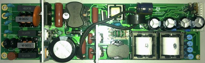
5 100W off-line LED lighting driver design
Based on UCC28810 (Transition mode PFC), UCC27510 (LLC controller for multi-string LED
lighting) and UCC28610 (auxiliary green mode Flyback controller), a 100W reference design
PMP4302A is developed. This design will drive 4 strings and 15 LEDs per string. The
dimensions for this demonstration board is 245mm(L)x18mm(W)x11mm(H), which is suitable for
high wattage general LED lighting form factor. Figure 8 shows a photo of the PMP4302A
reference design board including input EMI filter, TM PFC stage, auxiliary power supply stage
and multi-string LLC stage. Table 1 gives the electrical specification for this reference design.
A New Off-line LED Lighting Driver Solution with Multi-Transformer LLC Control 11SLUA617A – September 2011 – Revised September 2011
5.1 Design Specification
Auxiliary Power
EMI Filter PFC Stage Multi-string LLC Stage
Figure 8. Demo board for PMP4302A reference design
12 A New Off-line LED Lighting Driver Solution with Multi-Transformer LLC ControlSLUA617A – September 2011 – Revised September 2011
Table 1. Electrical Design Specification
Specification Items Min Typical Max
Input AC Voltage 90Vac 220Vac 264Vac
Output Voltage Tolerance 54Vdc 60Vdc
Number of LED strings 4
Output current per string 485mA 500mA 515mA
Output current tolerance +-3%
per string
PWM dimming range 1% 100%
Power Factor (90Vac~264Vac) 0.95 0.98 0.99
Efficiency @ 100% dimming 88% 91.5%
Turn-on Delay 200ms
Output String Open Loop Yes
Output String Over-voltage 60Vdc
w/ latch off
Output String Under-voltage 40Vdc
w/ latch off
Output String Short Yes
Maximum Input Current 1.3A
@ 90Vac 100% dimming light
Primary over current 2A
A New Off-line LED Lighting Driver Solution with Multi-Transformer LLC Control 13SLUA617A – September 2011 – Revised September 2011
5.2 Schematics
Figure 9. PFC stage schematic for PMP4302A
14 A New Off-line LED Lighting Driver Solution with Multi-Transformer LLC ControlSLUA617A – September 2011 – Revised September 2011
Figure 10. Multi-string LLC stage schematic of PMP4302A
A New Off-line LED Lighting Driver Solution with Multi-Transformer LLC Control 15SLUA617A – September 2011 – Revised September 2011
Figure 11. Auxiliary Flyback stage schematic of PMP4302A
5.3 Output Current Matching
Because of transformer’s magnetic balance with primary windings in series, the multi-
transformer LLC converter can achieve good current matching performance. There are two
considerations to improve current matching performance between the strings:
1. It is recommended to set the operating frequency above resonance when at nominal input
voltage range of the LLC converter. This improves LED current matching and transient
response during dimming. This will also make the output current operate in continuous
current mode, and it will have a much smaller difference in current between each string.
2. In a real transformer, the magnetizing current of the transformer has an influence on output
current matching. A smaller magnetizing current will have good current matching
performance. It is important to set the equivalent magnetizing inductance of the transformer
as high as possible to minimize the magnetizing current.
Table 2 gives the output current on each LED string with input voltage from 90Vac to 264Vac at
100% dimming. Table 3 also shows the output current but with PWM dimming duty cycle from
5% to 100% at 90Vac, 230Vac and 264Vac input. The output current matching tolerance is less
than +-3% according to the below data.
16 A New Off-line LED Lighting Driver Solution with Multi-Transformer LLC ControlSLUA617A – September 2011 – Revised September 2011
Table 2. Output current with input voltage
Vin Io1(A) Io2(A) Io3(A) Io4(A)
90 0.5086 0.5065 0.5064 0.5023
100 0.5083 0.5063 0.5068 0.5025
110 0.5081 0.5062 0.5067 0.5028
130 0.5081 0.5061 0.5077 0.5029
160 0.5079 0.5057 0.5073 0.503
180 0.5077 0.5056 0.5073 0.503
200 0.5076 0.5055 0.5075 0.5032
220 0.5076 0.5054 0.5074 0.5032
230 0.5077 0.5055 0.5076 0.5033
264 0.5078 0.5056 0.5075 0.5031
Table 3. Output current with PWM dimming and input voltage
90Vin
Dimming Io1(mA) Io2(mA) Io3(mA) Io4(mA) Max(mA) Min(mA) Ave(mA) %
5% 25.1 24.6 25.8 25.7 25.8 24.6 25.3 2.371542
10% 50.4 49.7 51.4 51.4 51.4 49.7 50.725 1.675702
20% 100.9 100.1 102.8 102.5 102.8 100.1 101.575 1.329067
30% 151.4 150.4 154.1 153.8 154.1 150.4 152.425 1.213712
40% 201.9 200.7 205.4 204.9 205.4 200.7 203.225 1.156354
50% 252.5 251 256.3 255.6 256.3 251 253.85 1.043924
60% 302.8 301.5 307.7 307.4 307.7 301.5 304.85 1.016894
70% 353.5 351.8 358.6 357.8 358.6 351.8 355.425 0.956601
80% 403.9 402.2 409.7 408.8 409.7 402.2 406.15 0.923304
90% 454.3 452.2 461.1 460.1 461.1 452.2 456.925 0.973902
99% 499.3 496.7 507.2 506.2 507.2 496.7 502.35 1.045088
100% 503.9 501.4 512.4 511.7 512.4 501.4 507.35 1.084064
230Vin
Dimming Io1(mA) Io2(mA) Io3(mA) Io4(mA) Max(mA) Min(mA) Ave(mA) %
5% 25.2 24.5 25.9 25.7 25.9 24.5 25.325 2.764067
10% 50.4 49.7 51.5 51.3 51.5 49.7 50.725 1.774273
20% 100.9 100.1 102.7 102.5 102.7 100.1 101.55 1.280158
30% 151.4 150.4 154.1 153.6 154.1 150.4 152.375 1.21411
40% 201.9 200.9 205.1 204.9 205.1 200.9 203.2 1.033465
50% 252.4 251.1 256.4 255.8 256.4 251.1 253.925 1.043615
60% 302.9 301.4 307.7 307 307.7 301.4 304.75 1.033634
70% 353.5 351.8 358.6 357.8 358.6 351.8 355.425 0.956601
80% 403.9 402.2 409.7 408.8 409.7 402.2 406.15 0.923304
90% 454.3 452.2 461.1 460.1 461.1 452.2 456.925 0.973902
99% 499.3 496.7 507.2 506.2 507.2 496.7 502.35 1.045088
100% 503.9 501.4 512.4 511.7 512.4 501.4 507.35 1.084064
A New Off-line LED Lighting Driver Solution with Multi-Transformer LLC Control 17SLUA617A – September 2011 – Revised September 2011
264Vin
Dimming Io1(mA) Io2(mA) Io3(mA) Io4(mA) Max(mA) Min(mA) Ave(mA) %
5% 25.1 24.6 25.8 25.7 25.8 24.6 25.3 2.371542
10% 50.4 49.7 51.4 51.4 51.4 49.7 50.725 1.675702
20% 100.9 100.1 102.8 102.5 102.8 100.1 101.575 1.329067
30% 151.4 150.4 154.1 153.8 154.1 150.4 152.425 1.213712
40% 201.9 200.7 205.4 204.9 205.4 200.7 203.225 1.156354
50% 252.5 251 256.3 255.6 256.3 251 253.85 1.043924
60% 302.8 301.5 307.7 307.4 307.7 301.5 304.85 1.016894
70% 353.5 351.8 358.6 357.8 358.6 351.8 355.425 0.956601
80% 403.9 402.2 409.8 408.6 409.8 402.2 406.125 0.935673
90% 454.3 452.4 461.1 460.3 461.1 452.4 457.025 0.951808
99% 499.4 496.7 507.2 506.2 507.2 496.7 502.375 1.045036
100% 503.9 501.4 512.4 511.7 512.4 501.4 507.35 1.084064
5.4 Efficiency
Efficiency is a key benefit for this solution. Efficiency is also related to component selection and
transformer design. The figure below is the efficiency curve for the PWM dimming version, and it
shows the highest efficiency is above 91%. For a non-dimming version only one schottky diode
is used for each string and there is no need for the PWM dimming MOSFET on the output side,
this can further improve overall efficiency by another 1~2%.
PMP4302A Efficiency
91.50%
91.00%
90.50%
90.00%
89.50%
89.00%
88.50%
88.00%
87.50%
87.00%
80 130 180 230 280
Input Voltage
Figure 12. Efficiency curve for PWM dimming version
18 A New Off-line LED Lighting Driver Solution with Multi-Transformer LLC ControlSLUA617A – September 2011 – Revised September 2011
5.5 Dimming waveform
This solution can support group PWM dimming from 1% to 100% range. In order to get a linear
dimming performance, the UCC25710 has a small delay time which allows the current loop to
maintain control at low PWM dimming duty cycles. Meanwhile, the DSR (Dimming Slew Rate)
function is used to control the rise and fall time of the VCO control voltage, allowing potentially
audible electro-mechanically induced noise to be minimized. Figure 13 shows the operating
waveforms during dimming. (CH1 yellow: LEDSW MOSFET Vgs 5V/Div; CH2 blue: LED Output
Current 1A/Div; CH3 red: DSR 2V/Div; CH4 green: Primary Current 1A/Div).
1% PWM Dimming 2% PWM Dimming
5% PWM Dimming 10% PWM Dimming
A New Off-line LED Lighting Driver Solution with Multi-Transformer LLC Control 19SLUA617A – September 2011 – Revised September 2011
20% PWM Dimming 30% PWM Dimming
40% PWM Dimming 50% PWM Dimming
80% PWM Dimming 90% PWM Dimming
Figure 13. Operating waveforms during PWM dimming
20 A New Off-line LED Lighting Driver Solution with Multi-Transformer LLC ControlSLUA617A – September 2011 – Revised September 2011
5.6 LLC stage waveforms
Figure 14 shows operating waveform for the LLC stage at full load, it shows the output current is
operating in CCM in order to achieve perfect current matching performance. Here, CH1 (yellow)
is Primary MOSFET Vds waveform with 100V/Div; CH2 (blue) is LED Output Current with
200mA/Div and CH4 (green) is primary current with 1A/Div.
90Vac input 230Vac input
Figure 14. LLC stage waveforms at full load
5.7 EMI performance
EMI is another benefit with this multi-string LLC topology. Figure 15 shows the test result for
conducted noise for this PMP4302A reference design.
A New Off-line LED Lighting Driver Solution with Multi-Transformer LLC Control 21SLUA617A – September 2011 – Revised September 2011
Figure 15. EMI conducted test results, EN55015 limits.
6 Conclusion
This application note presents a new multi-transformer LLC topology for general LED lighting. It
demonstrates high efficiency and PWM dimming. A 100W LED lighting driver to drive 4 LED
strings verified the performance for this proposed topology.
References
1. UCC25710 datasheet, Texas Instruments (SLUSAD7A)
2. UCC28810 datasheet, Texas Instruments (SLUS865)
3. UCC28610 datasheet, Texas Instruments (SLUS888D)
22 A New Off-line LED Lighting Driver Solution with Multi-Transformer LLC ControlIMPORTANT NOTICE
Texas Instruments Incorporated and its subsidiaries (TI) reserve the right to make corrections, modifications, enhancements, improvements,
and other changes to its products and services at any time and to discontinue any product or service without notice. Customers should
obtain the latest relevant information before placing orders and should verify that such information is current and complete. All products are
sold subject to TI’s terms and conditions of sale supplied at the time of order acknowledgment.
TI warrants performance of its hardware products to the specifications applicable at the time of sale in accordance with TI’s standard
warranty. Testing and other quality control techniques are used to the extent TI deems necessary to support this warranty. Except where
mandated by government requirements, testing of all parameters of each product is not necessarily performed.
TI assumes no liability for applications assistance or customer product design. Customers are responsible for their products and
applications using TI components. To minimize the risks associated with customer products and applications, customers should provide
adequate design and operating safeguards.
TI does not warrant or represent that any license, either express or implied, is granted under any TI patent right, copyright, mask work right,
or other TI intellectual property right relating to any combination, machine, or process in which TI products or services are used. Information
published by TI regarding third-party products or services does not constitute a license from TI to use such products or services or a
warranty or endorsement thereof. Use of such information may require a license from a third party under the patents or other intellectual
property of the third party, or a license from TI under the patents or other intellectual property of TI.
Reproduction of TI information in TI data books or data sheets is permissible only if reproduction is without alteration and is accompanied
by all associated warranties, conditions, limitations, and notices. Reproduction of this information with alteration is an unfair and deceptive
business practice. TI is not responsible or liable for such altered documentation. Information of third parties may be subject to additional
restrictions.
Resale of TI products or services with statements different from or beyond the parameters stated by TI for that product or service voids all
express and any implied warranties for the associated TI product or service and is an unfair and deceptive business practice. TI is not
responsible or liable for any such statements.
TI products are not authorized for use in safety-critical applications (such as life support) where a failure of the TI product would reasonably
be expected to cause severe personal injury or death, unless officers of the parties have executed an agreement specifically governing
such use. Buyers represent that they have all necessary expertise in the safety and regulatory ramifications of their applications, and
acknowledge and agree that they are solely responsible for all legal, regulatory and safety-related requirements concerning their products
and any use of TI products in such safety-critical applications, notwithstanding any applications-related information or support that may be
provided by TI. Further, Buyers must fully indemnify TI and its representatives against any damages arising out of the use of TI products in
such safety-critical applications.
TI products are neither designed nor intended for use in military/aerospace applications or environments unless the TI products are
specifically designated by TI as military-grade or "enhanced plastic." Only products designated by TI as military-grade meet military
specifications. Buyers acknowledge and agree that any such use of TI products which TI has not designated as military-grade is solely at
the Buyer's risk, and that they are solely responsible for compliance with all legal and regulatory requirements in connection with such use.
TI products are neither designed nor intended for use in automotive applications or environments unless the specific TI products are
designated by TI as compliant with ISO/TS 16949 requirements. Buyers acknowledge and agree that, if they use any non-designated
products in automotive applications, TI will not be responsible for any failure to meet such requirements.
Following are URLs where you can obtain information on other Texas Instruments products and application solutions:
Products Applications
Audio www.ti.com/audio Communications and Telecom www.ti.com/communications
Amplifiers amplifier.ti.com Computers and Peripherals www.ti.com/computers
Data Converters dataconverter.ti.com Consumer Electronics www.ti.com/consumer-apps
DLP® Products www.dlp.com Energy and Lighting www.ti.com/energy
DSP dsp.ti.com Industrial www.ti.com/industrial
Clocks and Timers www.ti.com/clocks Medical www.ti.com/medical
Interface interface.ti.com Security www.ti.com/security
Logic logic.ti.com Space, Avionics and Defense www.ti.com/space-avionics-defense
Power Mgmt power.ti.com Transportation and Automotive www.ti.com/automotive
Microcontrollers microcontroller.ti.com Video and Imaging www.ti.com/video
RFID www.ti-rfid.com
OMAP Mobile Processors www.ti.com/omap
Wireless Connctivity www.ti.com/wirelessconnectivity
TI E2E Community Home Page e2e.ti.com
Mailing Address: Texas Instruments, Post Office Box 655303, Dallas, Texas 75265
Copyright © 2011, Texas Instruments IncorporatedYou can also read


