Compact gate-based read-out of multiplexed quantum devices with a cryogenic CMOS active inductor - arXiv.org
←
→
Page content transcription
If your browser does not render page correctly, please read the page content below
Compact gate-based read-out of multiplexed quantum devices with a
                                           cryogenic CMOS active inductor
                                                       L. Le Guevel,1, 2, a) G. Billiot,1 S. De Franceschi,2 A. Morel,1 X. Jehl,2 A.G.M. Jansen,2 and G. Pillonnet1
                                                       1) Univ.   Grenoble Alpes, CEA, LETI, F-38000 Grenoble, France
                                                       2) Univ.   Grenoble Alpes, CEA, Grenoble INP, IRIG, PHELIQS, F-38000 Grenoble, France
                                                       (Dated: February 10, 2021)
                                                       In the strive for scalable quantum processors, significant effort is being devoted to the development of cryogenic clas-
                                                       sical hardware for the control and readout of a growing number of qubits. Here we report on a cryogenic circuit
                                                       incorporating a CMOS-based active inductor enabling fast impedance measurements with a sensitivity of 10 aF and an
                                                       input-referred noise of 3.7 aF/sqrt(Hz). This type of circuit is especially conceived for the readout of semiconductor
                                                       spin qubits. As opposed to commonly used schemes based on dispersive rf reflectometry, which require mm-scale
arXiv:2102.04364v2 [quant-ph] 9 Feb 2021

                                                       passive inductors, it allows for a markedly reduced footprint (50µm × 60µm), facilitating its integration in a scalable
                                                       quantum-classical architecture. In addition, its active inductor results in a resonant circuit with tunable frequency and
                                                       quality factor, enabling the optimization of readout sensitivity.

                                              An ingenious use of the laws of quantum mechanics has led            the qubit, which is commonly done through rf reflectome-
                                           to a new computing paradigm, generally known as quantum                 try. The inductive element of this tank circuit consists of a
                                           computing, that promises exponential speed-up in the solution           surface-mount inductor or a microfabricated superconducting
                                           of certain types of problems1–3 . Using a prototypical quantum          coil. Even for this second case, the corresponding footprint
                                           processor with 53 operational superconducting quantum bits              is relatively large (∼ mm2 ) and hence hardly compatible with
                                           (qubits), a ground-breaking experiment was recently able to             large-scale qubit integration.
                                           perform a first experiment towards quantum supremacy4, trig-               Here we propose an alternative readout technique involv-
                                           gering more extensive research on such a goal5 . Practical im-          ing a cryogenic CMOS-based active inductor with a compact
                                           plementations of quantum computing, however, are expected               design. Besides its reduced footprint favoring scalability, this
                                           to require much larger numbers of physical qubits6 .                    CMOS inductor offers the possibility to tune the characteris-
                                              Solid-state implementations seem to offer the best scalabil-         tic frequency and the quality factor of the resonator, which is
                                           ity prospects. While superconducting qubits are currently the           instrumental in optimizing measurement sensitivity. As op-
                                           leading platform, semiconductor spin qubits are emerging as a           posed to conventional reflectometry, our method consists in
                                           serious contender owing to the possibility to leverage the inte-        measuring the tank impedance at resonance. The cryogenic
                                           gration capabilities of silicon technology7. In both cases, the         read-out circuit is composed of a current source exciting the
                                           quantum processor can only function at very low temperature,            LC tank, an amplifier to read the voltage response, and a mul-
                                           typically below 0.1 K (only recently, it was shown that silicon         tiplexed capacitor bank to select different devices under test
                                           qubits could be operated even above 1 K with limited loss of            (DUT). We characterized the circuit sensitivity and tunability
                                           fidelity8,9 ).                                                          at 4.2 K demonstrating its capability to measure capacitances
                                              In a scale-up prospect toward increasingly large numbers             as low as 10 aF. By applying our technique to a gate-coupled
                                           of qubits, the introduction of classical cryogenic electron-            MOSFET co-integrated on the same chip we reveal typical
                                           ics positioned as close as possible to the qubits is widely             signatures of quantized electronic states.
                                           considered as a necessity. Various solutions have been pro-
                                           posed and partly demonstrated to a first proof-of-concept
                                           level. These include low-temperature (de)multiplexers10,11 ,            I.   IMPEDANCEMETRY
                                           analog-to-digital and digital-to-analog converters12,13 , low-
                                           noise amplifiers14,15 , RF oscillators16,17 , transimpedance               Capacitive spectroscopy of gate-controlled quantum-dot
                                           amplifiers18,19 , and digital processors20,21 . In a DRAM-like          devices allows the detection of electronic quantum states
                                           strategy22,23 , these cryogenic components can significantly re-        within the structure, including the firstly occupied electron
                                           duce the number of electrical lines running through the host            states. For enhanced detection sensitivity at high speed, the
                                           cryostat, thereby limiting the associated heat load and increas-        gate capacitance of the device under test (DUT), represented
                                           ing interconnect reliability. A CMOS-based cryogenic con-               as a single-electron transistor in Figure 1b, is connected to an
                                           troller operating at 3K was recently reported enabling high-            inductance to form an LC resonator. In a gate-coupled read-
                                           fidelity operations on an electron-spin two-qubit system24 . As         out scheme of the quantum state, the response of the tank at
                                           far as qubit readout is concerned, however, relatively little has       cryogenic temperature excited near resonance frequency fr is
                                           been done. Measuring the qubit state requires detecting small           conveyed back to room temperature for probing and analysis,
                                           variations in the impedance of an LC tank circuit coupled to            usually with homodyne I-Q detection. The phase of the tank
                                                                                                                   response becomes an image of the change in DUT capacitance
                                                                                                                   ∆C ≪ C p (see Figure 1a) through the relation ∆φ = Q∆C/C p
                                                                                                                   around fr with Q the resonator quality factor and C p the par-
                                           a) Electronic   mail: loick.leguevel@gmail.com                          allel capacitance.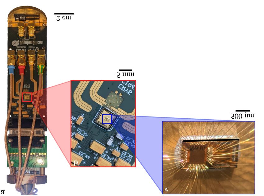
2

❈                                  ✿                                               ✿
                                    ❀                                               ❀                                     duce parasitic capacitance C par . Main amplification is placed
      ❇ ❄                                                           ❇ ❄
          ❄                                                             ❄                                                 at a higher temperature (typically 4.2 K) to benefit from higher
      ❇❃                                                       ■❇
                                                       ❅
                                                                                                                          cooling power.
                                                                                                                      ❅
                                                ❁❂
                                                                                                                             Impedancemetry has the advantage over reflectometry that
              ❄❄                                                            ❄❄                             ❁❂
      ❃                                                        ■                                                          the 50 Ω impedance matching plays no role in the optimiza-
                                                       ❅                                                              ❅
                                                                                                                          tion of the resonant circuit depending on the inductor and
                                        ❅❆                                              ❅❆
                                                                                                                          the parasitic capacitors. However, the cryogenic circuitry re-
                       ✶✷✸✷✹✺✻✼✷✺✽✾                                              ❉✼❊✷❋●❍✹✷✼✷✺✽✾
                                                                                                                          quired by impedancemetry generates extra noise compared to
                   ✁                    ✵                                          ✵              ✁
 ✴                     ✂                                                                              ✂                   reflectometry, which needs to be minimized. The impedance
                                                                                                                          of the resonator naturally filters out-of-resonance components
                                                      ✪✝✝ ✦
           ✟
            ✠✡
                                                                                                                ✟
                                                                                                                 ✠✡
                                                                                                                          (see Figure 1a) such as low-frequency flicker noise from elec-
                                                                                                                          tronics. In the perspective of quantum computing involving a
                                                      ✧★✩ ✦                                                               qubit matrix, Vin could contain a comb of excitation frequen-
                                                                                                                          cies to excite a set of frequency-selective resonators (see Sup-
                                                                                                                          plementary Material I with an estimation of the scaling for
                                                      ✥✄✦                              ✆✝✞
                                                                                                                          large qubit arrays).
                                                                                                                             In the case of impedancemetry, without the need of direc-
                                                                                 ✄☎✄                                      tional couplers, the footprint of the read-out circuitry is re-
                                             ✬ ✟                                                                          duced. Using modern CMOS technologies with sub-100nm
                                              ✭✭ ✠✡

                           ✆✝✞                                ✮ ✟
                                                               ✭✭ ✠✡                             ✠✡
                                                                                                      ✯✰ ✟
                                                                                                        ✱ ✠✡
                                                                                                                          nodes, the additional circuitry of current sources and follow-
                                                                                                                          ers easily fits on a chip with size comparable to the hundreds
     ✟☛☞
                                                  ✣✜✙✜✢✑✘✑✗
                                                                                                          ✟☛☞             of qubits chip (
3
III. INTEGRATED CIRCUIT DESIGN from possible instabilities. To tune the Q factor, we choose to
cover a wide range of CR values in steps of 23 fF by selecting
4 binary-weighted MOM capacitors of 23, 46, 92, and 184 fF.
The impedancemetry experiment was integrated on a sin-
From room-temperature simulations, these settings allow to
gle chip with multiplexed quantum devices using the Fully-
cover a wide range of quality factors Q from 7 to 300, includ-
Depleted Silicon-On-Insulator (FD-SOI) 28nm CMOS tech-
ing the unstable states with negative Q (see Supplementary
nology. The FD-SOI technology is very well suited for high-
Material III).
speed cryogenic applications29 with lower variability than
bulk technologies30, less sensitivity to carrier freeze-out, and The voltage-controlled current source exciting the resonator
threshold-voltage tuning with the use of the back-gate31. The is made of a current mirror combined to an RC bias tee. The
integration of classical circuitry with small-enough transistors bias tee superimposes DC signals from the diode transistor
that exhibit quantum properties is a plus to validate efficiently to set the DC operating point of the current source and AC
new circuit architectures16,19,32 signals from the excitation input Vin to generate the AC cur-
rent Iin . The RC filter of the bias tee consists of Rbt (polysili-
The realized integrated circuit contains the current source, con resistor of 10 MΩ) and Cbt (MOM capacitor of 406 fF) to
the active inductance with addressable capacitor banks for reach a characteristic frequency of 39 kHz. As no large signals
tunability, the multiplexed DUTs, and the amplification stage Vin are required, the current source operates in subthreshold
(Figure 2a, b). During design, we focused on bringing down regime with a bias current of only 0.1 µA to minimize its con-
the footprint and power consumption of the active inductance ductance for a negligible impact on the resonator and obtain
being the main original component of our circuit. The com- a desirable low transconductance for nA-current excitation.
plete amplification and current generation was added on-chip From foundry models, we get for the current generating tran-
to facilitate testing the concept of impedancemetry at 4.2 K. sistor a transconductance Gm of 3.4 nA/mV and bandwidth of
In the absence of high-frequency models of FD-SOI transis- 3.5 GHz (see Supplementary Material III).
tors at cryogenic temperatures, we designed the integrated cir- To investigate the active inductance circuit with different
cuit with accurate room-temperature models supplied by the DUTs, we added an addressable bank of 6 capacitors. Three
foundry33. The evolution of transistor characteristics towards MOM capacitors of 2, 4, and 8 fF have the purpose of cali-
the lowest temperatures was extrapolated from the tempera- brating the active inductance on known values. Three addi-
ture variation in foundry models but also from acquired 4.2 K tional MOSFETs (M0, M1, M2) of width 80 nm and length
data of single transistors30,31 . 28, 60, and 120 nm are used as test-bench for the investigation
The active inductance follows a known NMOS-based of quantum properties. The source and drain voltage of the
Karsilayan-Schaumann architecture34,35 . The gyrator is made quantum MOSFETs are grounded when unselected and polar-
of a single-ended negative transconductance −Gm,1 and a ized at Vbias when selected. The differential transconductance
differential transconductance stage Gm,2 . The gyrator trans- stage of the active inductance copies the DC common-mode
forms a tunable capacitance CL into an inductance L(CL ) = voltage Vcm to the DUT gate potential, such that the DC gate
CL /Gm,1 Gm,2 . An added metal-oxide-metal (MOM) capaci- voltage Vgs = Vcm −Vbias can be varied via Vbias (see Figure 2).
tor C p of 136
p fF parallel to L controls the resonant frequency Once excited by Iin , the tank voltage is amplified, then sent
fr = 1/2π L(CL )C p . No dependence in temperature is ex- through a unit-gain buffer for detection at room temperature
pected for MOM capacitors36. Adding C p makes the measur- via meter-long cable. The amplifier is a common-source N-
ing circuit less sensitive to the DUT-capacitance with the in- type single-stage and the 1:1 buffer is a common-drain N-type
creased tank capacitance but avoids the influence of unknown single stage (see Figure 2a). Based on room-temperature sim-
parasitic capacitances at cryogenic temperatures (e.g. sub- ulations, the amplifier has a gain A of 15 dB and a bandwidth
strate parasitics). Hence, the resonant frequency fr is set by of 1.8 GHz for a power consumption of 150 µW. The buffer
C p , CL , and Gm,i=1,2 . CL is implemented with one main metal- reaches a bandwidth of 92 MHz for a cable capacitance of
oxide-metal (MOM) capacitor of 362 fF in parallel with two 50 pF and a power consumption of 2.4 mW. The net ampli-
digitally-controlled binary-weighted MOM capacitors of 68 fication at 165 MHz becomes 8 dB.
and 136 fF (see Supplementary Material II). At room temper- Transistor noise translates into transconductance noise that
ature, the emulated L ranges from 5.3 to 8.4 µH to reach fr generates perturbing variations into the parameters determin-
from 128 to 165 MHz (see Supplementary Material III). The ing the active inductance. A varying L modulates fr and
estimated power consumption of the resonator is 85 µW and generates phase noise in Vout . The phase noise spectrum of
corresponds to a footprint of 8.5 µW/qubit assuming a 10 × 10 Vout around the carrier frequency fr extracted from room-
frequency-multiplexed array of qubits with frequency resolu- temperature steady-state simulations (SST) exhibits a flicker
tion of 5 MHz in a 1 GHz bandwidth. component (see Supplementary Material III) on time-scale
Adding a capacitance CR at the foot of the differential >10 ms, induced by a noisy modulated L. For a typical Q of
transconductance stage allows to introduce a negative re- 81 with sufficiently fast measurements
√ to avoid 1/ f noise, we
sistance in series with the active inductance, leading to get a phase noise√of 0.002 °/ Hz that gives an input-referred
higher Q-factor with an increased parallel effective resistance noise of 3.2 aF/ Hz.
R(CR ,CL ). ThepQ-factor of the active inductance defined as Voltage excitation and homodyne detection are performed
Q = R(CL ,CR ) L(CL )/C p depends on CR and CL . By tuning at room temperature with an all-digital lock-in amplifier (Fig-
CL , then CR , L and Q can be adjusted to any desired value apart ure 2c). Different configurations for single (I) and double4
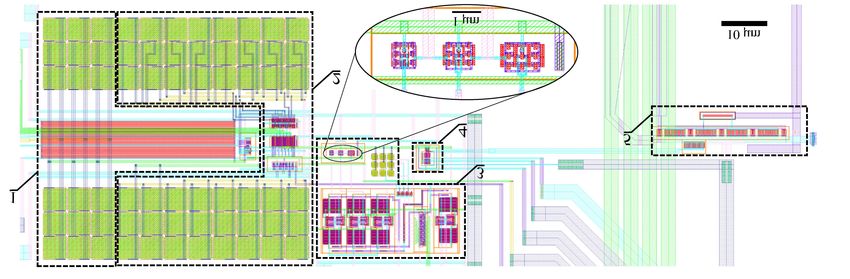
Figure 2. Setup with on-chip electronics. a, On-chip circuit implementation of the active inductance (pink), current excitation (green),
test capacitor bank (blue), and amplification stage (red). For clarity, the bias MOSFETs operating in DC are drawn of smaller size than
MOSFETs in the high-frequency signal chain. b, Simplified view of the on-chip resonant circuit placed at 4.2 K with tunable resonator,
DUT, current excitation, and voltage amplification, linked to room-temperature phase-sensitive electronics via meter-long cables. c, Room-
temperature homodyne detection with single (I) and double (II) demodulation of the circuit output Vout and generation of voltage excitation
Vin at modulation frequencies f1 (150-200 MHz) and f2 (1 kHz).
(II a,b) demodulation are further described in the following 199.0 MHz by tuning CL . The quality factors Q extracted from
section when needed. a linear fit of the phase around fr are shown in Figure 3b. The
Q values range from 80 to 250, and can be tuned by a fac-
tor > 2 for every CL by adjusting CR . These data demonstrate
IV. IMPEDANCEMETRY CIRCUIT CHARACTERIZATION that Q can be tuned almost independently of the resonance fre-
quency with a frequency variation of less than 0.22 % across
Without the assistance of low-temperature models, the op- the entire CR range (see Figure 3b).
erating point of the circuit had to be determined experimen- For the minimum value of CL with the highest resonance
tally starting from room-temperature settings of bias voltages frequency, we calibrate the capacitance sensitivity of the cir-
and currents. The increase in threshold voltage of NMOS cuit for each Q by switching on and off the DUT MOM capac-
(resp. PMOS) transistors at 4.2 K is compensated by apply- itors Cm =2, 3, and 8 fF and using double homodyne detection
ing a back-gate voltage of 1.2 V (resp. −2 V). The optimal (II a) (see Figure 3c). The capacitance sensitivity α is ex-
cryogenic common-mode voltage Vcm = 0.48 V was obtained tracted from a least-square linear fit of the phase change ∆φ =
while monitoring the tank impedance via repeated frequency QCm /C p ≡ α Cm for a given Q as shown in Figure 3d. The
sweeps until a typical resonance behavior up to 200 MHz sensitivity α increases linearly with Q from 0.76 to 1.9 °/fF.
emerges for the lowest values of CL and CR . The gain of the From the linear fit in Figure 3d, we obtain C p = 137 fF, in
low-temperature amplification stage at fr is optimized with good agreement with the designed value (136 fF). In usual
respect to the curent bias of amplifier and buffer (see Supple- circuits without an additional input capacitance34, the para-
mentary Material IV). The main results of the impedanceme- sitic capacitance of the MOSFETs determines the resonance
try with respect to tunability and detection sensitivity are frequency. In future design with accurate cryogenic compact
shown in Figure 3. models, this capacitance can be reduced significantly leading
The amplitude and phase of Vout using single homodyne de- to higher resonance frequency and improved sensitivity.
tection (I) without any connected DUT are shown in Figure 3a From C p and fr , we are now able to deduce the inductance
for the 4 CL values from 362 to 566 fF and two CR values cho- value L. By adjusting CL , L varies from 2.42 to 5.18 µH.
sen between 0 and 322 fF depending on CL . Vout at maximal For a total footprint of 60 µm × 50 µm, the active inductance
amplitude was kept equal to 1.8 mV by adjusting Vin to avoid density of 1.73 mH/mm2 is five orders of magnitude higher
non-linearities coming from non-linear MOSFETs behavior. than previously used passive inductors (55 nH/mm2)25 and
The resonance frequency fr varies by 5.1 % from 189.1 to three orders of magnitude higher than superconding inductors5
Figure 3. Characterization of the resonant circuit at 4.2 K for capacitance detection. a, Amplitude and phase of the demodulated circuit
output Vout for several active inductance settings. The resonance frequency shifts to lower frequency as the inductance value increases with
increasing CL (different colors). The continuous line (low-Q) and dashed line (high-Q) show the signals for different values of CR . b, Data
points for the resonance frequency fr when the extracted Q is tuned with CR . The colored bars of width given by the written maximal deviation
indicate the low dispersion of fr for fixed CL when varying Q with CR . c, Measured phase shift for MOM capacitor Cm of 2, 4, and 8 fF in
several Q-factor settings. The capacitance sensitivity ∆φ /Cm of the circuit is extracted from the slope with a least square fit at given Q. d,
Capacitance sensitivity extracted from c as a function of the Q factor. A least square linear fit of ∆φ /Cm (Q) allows to extract the capacitance
Cp parallel with the active inductance.
(1.6 µH/mm2 )37 . tors, we add a second demodulation (IIa) at the capacitance
switching frequency of 1 kHz to remove phase noise originat-
ing from a varying L. The 1 kHz square-wave φ from (I) with
V. CAPACITANCE RESOLUTION an integration time of 100 µs is demodulated by (IIa) at 1 kHz
to obtain its amplitude |φ |. The capacitance resolution as a
We now turn to the resolution in capacitance of the set-up, function of the second integration time for the 1 kHz demod-
√
we derive the input-referred noise in aF/ Hz from the signal- ulation is extracted by taking the ratio of the average and the
to-noise ratio (SNR) as a function of the integration time tint . standard deviation of the |φ | signal and is shown in Figure 4.
For this, we generate a capacitance change by continuously With an integration time of 1 s, the resolution becomes as low
connecting and disconnecting Cm = 2 fF at a rate of 1 kHz. as 10 aF.
Using the demodulation method (I), the square-wave of the
phase φ at fr with a rise time given by the integration time
is used to extract the signal power Psig and noise power Pnoise VI. QUANTUM CAPACITANCE MEASUREMENTS
by separating the corresponding frequency components in the
power spectrum (see Supplementary Material IV). The result- With the calibrated impedancemetry circuit, we are able to
ing SNR= Psig /Pnoise is used to extract the capacitance resolu- detect the gate quantum capacitance Cgg of the multiplexed
tion given by the equivalent Cm (SNR = 1) = Cm /SNR shown tiny MOSFETs (M0, M1, M2 in Figure 2a) similar to the
in Figure 4 as a function of tint from 100 ns to 100 µs. A ones used to implement spin qubits7 or single-electron tran-
capacitance of 1 fF can be detected with an integration time sistors for read-out with CMOS technology. Measurements
of 1 µs with SNR = 1. The capacitance resolution follows a will be presented for M2 with a gate length of 120 nm and a
square-root law with tint from which √ we extract the equiva- gate width of 80 nm. The other available device shows similar
lent input-referred noise of 3.7 aF/ Hz, two orders of mag- behavior (see Supplementary Material V).
nitude higher than the best reported sensitivity using an ultra- The total gate capacitance Cgg of such devices corresponds
low noise SQUID amplifier38. to the sum of the capacitance to drain, source, back-gate, and
As correlated noise appears on time scales longer than 1 ms MOSFET channel of which the gate to channel capacitance
originating probably from the 1/ f flicker noise of the transis- depends highly on the gate-source voltage Vgs controlled by6
pling increases with Vgs from 10 to 14 as the electron-filled
inversion layer is brought back to the top-interface.
These measurements of integrated quantum devices demon-
strate that the capacitive signature of structure in the elec-
tronic density of states of quantum dots can be probed via
impedancemetry.
VII. CONCLUSIONS
We reported an integrated circuit that performs
impedancemetry of a resonator coupled to a quantum
dot at cryogenic temperatures. The active inductance of the
resonator allowed the controlled tuning of the resonance
Figure 4. Capacitance resolution of the measurement set-up. Ex- frequency and quality factor, which will be of importance
trapolated capacitance Cm at signal-to-noise ratio equal to 1 for sin- for optimal frequency-spectrum crowding in multiplexed
gle (I) (black circles) and double (IIa) (red squares) homodyne de- read-out schemes. The employed multiplexing of nanometric
tection of the capacitance measurement as a function of the inte- quantum devices with on-chip switches could be beneficial
−1/2 for reduced power per qubit in a scalable multi-qubit architec-
gration time tint . Dashed lines are least-square fits Cm = a tint
√ ture. Novel read-out architectures with cryogenic electronics,
with√a = 0.250 Sc and Sc the equivalent noise spectral density in
aF/ Hz of the capacitance measurement. such as the active inductance, have the potential to increase
scalability and flexibility in the design and exploitation of
quantum processors.
the DC component of Vbias (see Figure 2a). As Cgg of nano- Further work towards lower noise and lower power design
metric devices is extremely small compared to C p , we don’t with more accurate high-frequency models at cryogenic tem-
expect to have sufficient SNR for small capacitance variations peratures will improve the final performance. Measuring mul-
at reasonable integration times. Better sensitivity can be ob- tiplexed out-of-chip capacitances of quantum devices will be
tained by modulating Vgs (method IIb) to measure after de- also promising for the screening of quantum devices with a
modulation the first derivative dCgg /dVgs as Cgg varies a lot in simpler experimental setup than reflectometry. In the long run,
a small Vgs window. the realization of tailored high-end analog electronics at cryo-
While the resonator impedance is probed at 199 MHz, Vgs genic temperatures will improve and accelerate the up-scaling
is modulated at 1 kHz with mV-range excitation on Vbias (see of quantum processors.
Figure 2bc). The obtained result with a relatively large 25 mV
Vgs modulation (shown in Figure 5a) is reminiscent of the
typical gate capacitance variation around threshold voltage
METHODS
Vth ≃ 0 V at Vbg = 6 V. Cgg (see inset of Figure 5a) reflects the
typical behavior for a FET capacitance from the subthreshold
regime Vgs ≪ Vth to the strong inversion regime Vgs ≫ Vth . Fabrication details. The impedancemetry chip was de-
Upon decreasing the amplitude of the Vgs modulation to only signed in a commercial CMOS FD-SOI 28nm technology
3.1 mV, the observed dCgg /dVgs signal in Figure 5b reveals with low-Vth (LVT) thin-oxide (GO1) transistors. The chip
a fine structure around Vth consisting of successive peak-dip is wire-bonded onto a QFN48 package directly soldered on a
oscillations. Following numerical integration, these features 4-layer PCB with FR4 substrate.
result in a series of peaks in Cgg , which we interpret as quan- Measurement set-up. The FR4 PCB is placed at the end of
tum contributions to the capacitance coming from electrons a dip-stick enclosed in a metallic container filled with a small
tunneling in and out of localized quantum states within the amount of helium gas for thermal exchange with a liquid He
transistor channel. bath (see Supplementary Material VI). A PCB-mounted ther-
To further identify these quantum states, we acquire mometer ensures a precise monitoring of the PCB tempera-
dCgg /dVgs for different back-gate voltage Vbg from 2 to 6 V ture. High-frequency lines of Vin and Vout are routed on the
as shown in Figure 5c. As Vbg increases, all observed features PCB from the chip package to the SMA coaxial connectors
shift to lower Vgs with a slope close to the ratio β of gate- via top-layer 50Ω-matched coplanar waveguide with ground
channel capacitance Cg−ch over the backgate-channel capaci- plane and via fencing. Supply lines are decoupled from
tance Cbg−ch alike the Vth -shift with back-gate for similar FET environmental noise with PCB-mounted capacitors (0.1, 1,
devices31. For Vbg > 4 V, all features have a coupling ratio of 10 µF) and conveyed to room temperature with copper wiring.
10 except for one with a lower coupling 8.6 attributed to an All other DC lines are conveyed to room-temperature with
impurity closer to the back-gate interface. No anomalous im- 50 − 130 Ω constantan wiring. At room temperature, elec-
purity structure is detected in the smaller 60 nm × 80 nm de- tronic apparatus comprises a multi-channel low-noise 21-bit
vice (see Supplementary Material V). At lower Vbg , the cou- digital-to-analog converter, and a 600 MHz lock-in amplifier.7
Figure 5. Quantum capacitance measurement of an integrated MOSFET with channel length 120 nm and width 80 nm. a, Measurement
of the first derivative of the gate capacitance Cgg with respect to Vgs by applying a gate-source AC excitation of 25 mV. The inset shows the
capacitance Cgg (Vgs ) computed from the integrated signal of the derivative. b, Expanded view of dCgg /dVgs around the off-on transition of the
MOSFET measured with a smaller excitation of 3.1 mV. The resolved features are signatures of quantized electronic states in the measured
capacitance of the MOSFET channel. c, Evolution of dCgg /dVgs with the back-gate voltage Vbg and the gate-source voltage Vgs . The indicated
slopes β = dVbg /dVgs ≃ Cg−ch /Cbg−ch represent the relative coupling strength of the detected quantized states with respect to back- and
front-gate.
DATA AVAILABILITY Rubin, Daniel Sank, Kevin J. Satzinger, Vadim Smelyanskiy, Kevin J. Sung,
Matthew D. Trevithick, Amit Vainsencher, Benjamin Villalonga, Theodore
White, Z. Jamie Yao, Ping Yeh, Adam Zalcman, Hartmut Neven, and
The data that support the plots within this paper and other John M. Martinis. Quantum supremacy using a programmable supercon-
findings of this study are available from the corresponding au- ducting processor. Nature, 574(7779):505–510, October 2019.
5 Yiqing Zhou, E. Miles Stoudenmire, and Xavier Waintal. What Limits the
thor upon reasonable request.
Simulation of Quantum Computers? Physical Review X, 10(4):041038,
November 2020.
6 Craig Gidney and Martin Ekerå. How to factor 2048 bit RSA integers in
REFERENCES 8 hours using 20 million noisy qubits. arXiv:1905.09749 [quant-ph], De-
cember 2019. arXiv: 1905.09749.
7 R. Maurand, X. Jehl, D. Kotekar-Patil, A. Corna, H. Bohuslavskyi, R. Lav-
1 Peter W. Shor. Polynomial-Time Algorithms for Prime Factorization and iéville, L. Hutin, S. Barraud, M. Vinet, M. Sanquer, and S. De Franceschi.
Discrete Logarithms on a Quantum Computer. arXiv:quant-ph/9508027, A CMOS silicon spin qubit. Nature Communications, 7:13575, November
January 1996. arXiv: quant-ph/9508027. 2016.
2 Lov K. Grover. Quantum Mechanics Helps in Searching for a Needle in a 8 Matias Urdampilleta, David J. Niegemann, Emmanuel Chanrion, Bap-
Haystack. Physical Review Letters, 79(2):325–328, July 1997. tiste Jadot, Cameron Spence, Pierre-André Mortemousque, Christopher
3 I.M. Georgescu, S. Ashhab, and Franco Nori. Quantum simulation. Reviews
Bäuerle, Louis Hutin, Benoit Bertrand, Sylvain Barraud, Romain Maurand,
of Modern Physics, 86(1):153–185, March 2014. Marc Sanquer, Xavier Jehl, Silvano De Franceschi, Maud Vinet, and Tristan
4 Frank Arute, Kunal Arya, Ryan Babbush, Dave Bacon, Joseph C. Bardin,
Meunier. Gate-based high fidelity spin readout in a CMOS device. Nature
Rami Barends, Rupak Biswas, Sergio Boixo, Fernando G. S. L. Brandao, Nanotechnology, 14(8):737–741, August 2019. Number: 8 Publisher: Na-
David A. Buell, Brian Burkett, Yu Chen, Zijun Chen, Ben Chiaro, Roberto ture Publishing Group.
Collins, William Courtney, Andrew Dunsworth, Edward Farhi, Brooks 9 C. H. Yang, R. C. C. Leon, J. C. C. Hwang, A. Saraiva, T. Tanttu, W. Huang,
Foxen, Austin Fowler, Craig Gidney, Marissa Giustina, Rob Graff, Keith J. Camirand Lemyre, K. W. Chan, K. Y. Tan, F. E. Hudson, K. M. Itoh,
Guerin, Steve Habegger, Matthew P. Harrigan, Michael J. Hartmann, Alan A. Morello, M. Pioro-Ladrière, A. Laucht, and A. S. Dzurak. Opera-
Ho, Markus Hoffmann, Trent Huang, Travis S. Humble, Sergei V. Isakov, tion of a silicon quantum processor unit cell above one kelvin. Nature,
Evan Jeffrey, Zhang Jiang, Dvir Kafri, Kostyantyn Kechedzhi, Julian Kelly, 580(7803):350–354, April 2020. Number: 7803 Publisher: Nature Pub-
Paul V. Klimov, Sergey Knysh, Alexander Korotkov, Fedor Kostritsa, David lishing Group.
Landhuis, Mike Lindmark, Erik Lucero, Dmitry Lyakh, Salvatore Mandrà, 10 D. R. Ward, D. E. Savage, M. G. Lagally, S. N. Coppersmith, and M. A.
Jarrod R. McClean, Matthew McEwen, Anthony Megrant, Xiao Mi, Kristel Eriksson. Integration of on-chip field-effect transistor switches with dopant-
Michielsen, Masoud Mohseni, Josh Mutus, Ofer Naaman, Matthew Neeley, less Si/SiGe quantum dots for high-throughput testing. Applied Physics
Charles Neill, Murphy Yuezhen Niu, Eric Ostby, Andre Petukhov, John C. Letters, 102(21):213107, May 2013.
Platt, Chris Quintana, Eleanor G. Rieffel, Pedram Roushan, Nicholas C.8 11 B. Paquelet Wuetz, P. L. Bavdaz, L. A. Yeoh, R. Schouten, H. van der Does, Zalba. A CMOS dynamic random access architecture for radio-frequency M. Tiggelman, D. Sabbagh, A. Sammak, C. G. Almudever, F. Sebastiano, readout of quantum devices. Nature Electronics, 2(6):236–242, June 2019. J. S. Clarke, M. Veldhorst, and G. Scappucci. Multiplexed quantum trans- 23 Andrea Ruffino, Tsung-Yeh Yang, John Michniewicz, Yatao Peng, Edoardo port using commercial off-the-shelf CMOS at sub-kelvin temperatures. npj Charbon, and Miguel Fernando Gonzalez-Zalba. Integrated multiplexed Quantum Information, 6(1):1–8, May 2020. Number: 1 Publisher: Nature microwave readout of silicon quantum dots in a cryogenic CMOS chip. Publishing Group. arXiv:2101.08295 [cond-mat, physics:physics, physics:quant-ph], January 12 H. Homulle, S. Visser, and E. Charbon. A Cryogenic 1 GSa/s, Soft-Core 2021. arXiv: 2101.08295. FPGA ADC for Quantum Computing Applications. IEEE Transactions 24 Xiao Xue, Bishnu Patra, Jeroen P. G. van Dijk, Nodar Samkharadze, Sushil on Circuits and Systems I: Regular Papers, 63(11):1854–1865, November Subramanian, Andrea Corna, Charles Jeon, Farhana Sheikh, Esdras Juarez- 2016. Conference Name: IEEE Transactions on Circuits and Systems I: Hernandez, Brando Perez Esparza, Huzaifa Rampurawala, Brent Carlton, Regular Papers. Surej Ravikumar, Carlos Nieva, Sungwon Kim, Hyung-Jin Lee, Amir Sam- 13 Joseph C. Bardin, Evan Jeffrey, Erik Lucero, Trent Huang, Sayan Das, mak, Giordano Scappucci, Menno Veldhorst, Fabio Sebastiano, Masoud Daniel Thomas Sank, Ofer Naaman, Anthony Edward Megrant, Rami Babaie, Stefano Pellerano, Edoardo Charbon, and Lieven M. K. Van- Barends, Ted White, Marissa Giustina, Kevin J. Satzinger, Kunal Arya, Pe- dersypen. CMOS-based cryogenic control of silicon quantum circuits. dram Roushan, Benjamin Chiaro, Julian Kelly, Zijun Chen, Brian Burkett, arXiv:2009.14185 [cond-mat, physics:physics, physics:quant-ph], Septem- Yu Chen, Andrew Dunsworth, Austin Fowler, Brooks Foxen, Craig Gidney, ber 2020. arXiv: 2009.14185. Rob Graff, Paul Klimov, Josh Mutus, Matthew J. McEwen, Matthew Nee- 25 A. Crippa, R. Ezzouch, A. Aprá, A. Amisse, R. Laviéville, L. Hutin, ley, Charles J. Neill, Chris Quintana, Amit Vainsencher, Hartmut Neven, B. Bertrand, M. Vinet, M. Urdampilleta, T. Meunier, M. Sanquer, X. Jehl, and John Martinis. Design and Characterization of a 28-nm Bulk-CMOS R. Maurand, and S. De Franceschi. Gate-reflectometry dispersive readout Cryogenic Quantum Controller Dissipating Less Than 2 mW at 3 K. IEEE and coherent control of a spin qubit in silicon. Nature Communications, Journal of Solid-State Circuits, 54(11):3043–3060, November 2019. Con- 10(1):2776, December 2019. ference Name: IEEE Journal of Solid-State Circuits. 26 Guoji Zheng, Nodar Samkharadze, Marc L. Noordam, Nima Kalhor, Del- 14 Shirin Montazeri, Wei-Ting Wong, Ahmet H. Coskun, and Joseph C. phine Brousse, Amir Sammak, Giordano Scappucci, and Lieven M. K. Van- Bardin. Ultra-Low-Power Cryogenic SiGe Low-Noise Amplifiers: Theory dersypen. Rapid gate-based spin read-out in silicon using an on-chip res- and Demonstration. IEEE Transactions on Microwave Theory and Tech- onator. Nature Nanotechnology, 14(8):742–746, August 2019. niques, 64(1):178–187, January 2016. Conference Name: IEEE Transac- 27 Fei Yuan. CMOS Active Inductors and Transformers. Springer US, Boston, tions on Microwave Theory and Techniques. MA, 2008. 15 B. Patra, R. M. Incandela, J. P. G. van Dijk, H. A. R. Homulle, L. Song, 28 A. Ilker Karsilayan and R. Schaumann. A high-frequency high-Q CMOS M. Shahmohammadi, R. B. Staszewski, A. Vladimirescu, M. Babaie, F. Se- active inductor with DC bias control. In Proceedings of the 43rd IEEE Mid- bastiano, and E. Charbon. Cryo-CMOS Circuits and Systems for Quantum west Symposium on Circuits and Systems (Cat.No.CH37144), volume 1, Computing Applications. IEEE Journal of Solid-State Circuits, 53(1):309– pages 486–489 vol.1, August 2000. 321, January 2018. 29 Lucas Nyssens, Arka Halder, Babak Kazemi Esfeh, Nicolas Planes, De- 16 Loick Le Guevel, Gerard Billiot, Xavier Jehl, Silvano De Franceschi, Mar- nis Flandre, Valeriya Kilchytska, and Jean-Pierre Raskin. 28-nm FD-SOI cos Zurita, Yvain Thonnart, Maud Vinet, Marc Sanquer, Romain Maurand, CMOS RF Figures of Merit Down to 4.2 K. IEEE Journal of the Electron Aloysius G. M. Jansen, and Gael Pillonnet. A 110mK 295µW 28nm FD- Devices Society, 8:646–654, 2020. Conference Name: IEEE Journal of the SOI CMOS Quantum Integrated Circuit with a 2.8GHz Excitation and nA Electron Devices Society. Current Sensing of an On-Chip Double Quantum Dot. In 2020 IEEE Inter- 30 Bruna Cardoso Paz, Loïck Le Guevel, Mikaël Cassé, Gérard Billiot, national Solid- State Circuits Conference - (ISSCC), pages 306–308, San Gaël Pillonnet, Aloysius Jansen, Sebastien Haendler, Andre Juge, Em- Francisco, CA, USA, February 2020. IEEE. manuel Vincent, Philippe Galy, Gérard Ghibaudo, Maud Vinet, Silvano de 17 Jiang Gong, Yue Chen, Fabio Sebastiano, Edoardo Charbon, and Masoud Franceschi, Tristan Meunier, and Fred Gaillard. Integrated Variability Mea- Babaie. 19.3 A 200dB FoM 4-to-5GHz Cryogenic Oscillator with an Au- surements of 28 nm FDSOI MOSFETs down to 4.2 K for Cryogenic CMOS tomatic Common-Mode Resonance Calibration for Quantum Computing Applications. In 2020 IEEE 33rd International Conference on Microelec- Applications. In 2020 IEEE International Solid- State Circuits Conference tronic Test Structures (ICMTS), pages 1–5, May 2020. ISSN: 2158-1029. - (ISSCC), pages 308–310, February 2020. ISSN: 2376-8606. 31 B Cardoso Paz, L Le Guevel, M Cassé, G Billiot, G Pillonnet, A G M 18 M. L. V. Tagliaferri, A. Crippa, S. Cocco, M. De Michielis, M. Fanciulli, Jansen, R Maurand, S Haendler, A Juge, E Vincent, P Galy, G Ghibaudo, G. Ferrari, and E. Prati. Modular Printed Circuit Boards for Broadband M Vinet, S de Franceschi, T Meunier, F Gaillard, and Institut Néel. Vari- Characterization of Nanoelectronic Quantum Devices. IEEE Transactions ability Evaluation of 28nm FD-SOI Technology at Cryogenic Temperatures on Instrumentation and Measurement, 65(8):1827–1835, August 2016. down to 100mK for Quantum Computing. IEEE Symposium on VLSI Tech- 19 L. Le Guevel, G. Billiot, B. Cardoso Paz, M. L. V. Tagliaferri, nology (In Press), 2020. S. De Franceschi, R. Maurand, M. Cassé, M. Zurita, M. Sanquer, M. Vinet, 32 S. Bonen, U. Alakusu, Y. Duan, M. J. Gong, M. S. Dadash, L. Lucci, D. R. X. Jehl, A. G. M. Jansen, and G. Pillonnet. Low-power transimpedance Daughton, G. C. Adam, S. Iordănescu, M. Pǎşteanu, I. Giangu, H. Jia, L. E. amplifier for cryogenic integration with quantum devices. Applied Physics Gutierrez, W. T. Chen, N. Messaoudi, D. Harame, A. Müller, R. R. Man- Reviews, 7(4):041407, December 2020. Publisher: American Institute of sour, P. Asbeck, and S. P. Voinigescu. Cryogenic Characterization of 22-nm Physics. FDSOI CMOS Technology for Quantum Computing ICs. IEEE Electron 20 Jeroen Petrus Gerardus Van Dijk, Bishnu Patra, Sushil Subramanian, Xiao Device Letters, 40(1):127–130, January 2019. Conference Name: IEEE Xue, Nodar Samkharadze, Andrea Corna, Charles Jeon, Farhana Sheikh, Electron Device Letters. Esdras Juarez-Hernandez, Brando Perez Esparza, Huzaifa Rampurawala, 33 T. Poiroux, O. Rozeau, P. Scheer, S. Martinie, M. Jaud, M. Minondo, Brent R. Carlton, Surej Ravikumar, Carlos Nieva, Sungwon Kim, Hyung- A. Juge, J. C. Barbé, and M. Vinet. Leti-UTSOI2.1: A Compact Model Jin Lee, Amir Sammak, Giordano Scappucci, Menno Veldhorst, Lieven for UTBB-FDSOI Technologies—Part II: DC and AC Model Descrip- M. K. Vandersypen, Edoardo Charbon, Stefano Pellerano, Masoud Babaie, tion. IEEE Transactions on Electron Devices, 62(9):2760–2768, September and Fabio Sebastiano. A Scalable Cryo-CMOS Controller for the Wide- 2015. band Frequency-Multiplexed Control of Spin Qubits and Transmons. IEEE 34 Haiqiao Xiao and Rolf Schaumann. A 5.4-GHz high-Q tunable active- Journal of Solid-State Circuits, pages 1–1, 2020. Conference Name: IEEE inductor bandpass filter in standard digital CMOS technology. Analog In- Journal of Solid-State Circuits. tegrated Circuits and Signal Processing, 51(1):1–9, April 2007. 21 E. Schriek, F. Sebastiano, and E. Charbon. A Cryo-CMOS Digital Cell 35 H. Barthelemy and W. Rahajandraibe. NMOS transistors based Karsilayan Library for Quantum Computing Applications. IEEE Solid-State Circuits Schaumann gyrator :’lowpass and bandpass filter applications’. In 2003 Letters, pages 1–1, 2020. Conference Name: IEEE Solid-State Circuits 46th Midwest Symposium on Circuits and Systems, volume 1, pages 97– Letters. 100 Vol. 1, December 2003. 22 Simon Schaal, Alessandro Rossi, Virginia N. Ciriano-Tejel, Tsung-Yeh 36 Bishnu Patra, Mohammadreza Mehrpoo, Andrea Ruffino, Fabio Sebas- Yang, Sylvain Barraud, John J. L. Morton, and M. Fernando Gonzalez- tiano, Edoardo Charbon, and Masoud Babaie. Characterization and Anal-
9

   ysis of On-Chip Microwave Passive Components at Cryogenic Temper-              Agreement No. 810504 (ERC Synergy project QuCube).
   atures. arXiv:1911.13084 [physics, physics:quant-ph], November 2019.
   arXiv: 1911.13084.
37
   J. M. Hornibrook, J. I. Colless, A. C. Mahoney, X. G. Croot, S. Blanvillain,
   H. Lu, A. C. Gossard, and D. J. Reilly. Frequency multiplexing for readout
   of spin qubits. Applied Physics Letters, 104(10):103108, March 2014.
38 F. J. Schupp, F. Vigneau, Y. Wen, A. Mavalankar, J. Griffiths, G. A. C.

   Jones, I. Farrer, D. A. Ritchie, C. G. Smith, L. C. Camenzind, L. Yu,
   D. M. Zumbühl, G. A. D. Briggs, N. Ares, and E. A. Laird. Radio-
   frequency reflectometry of a quantum dot using an ultra-low-noise SQUID
   amplifier. arXiv:1810.05767 [cond-mat, physics:physics, physics:quant-
   ph], June 2020. arXiv: 1810.05767.

                                                                                  COMPETING INTERESTS
ACKNOWLEDGEMENTS

  This work was partly supported by the European Union’s                            The authors declare a patent application FR1914651, filed
Horizon 2020 research and innovation program under Grant                          on december 17th 2019.
Supplementary Material: Compact gate-based read-out of multiplexed
quantum devices with a cryogenic CMOS active inductor
L. Le Guevel,1, 2, a) G. Billiot,1 S. De Franceschi,2 A. Morel,1 X. Jehl,2 A.G.M. Jansen,2 and G. Pillonnet1
1) Univ. Grenoble Alpes, CEA, LETI, F-38000 Grenoble, France
2) Univ. Grenoble Alpes, CEA, Grenoble INP, IRIG, PHELIQS, F-38000 Grenoble, France
(Dated: February 10, 2021)
arXiv:2102.04364v2 [quant-ph] 9 Feb 2021
I. READ-OUT SCALING OF LARGE QUBIT ARRAYS
Element Footprint Scaling
(mm2 )
Qubits 10−8 m × N2
Amplifiers 0.1 m
Inductors 1 m×N
Couplers 100 m
Figure S1. Reflectometry and scaling of large qubit arrays using directionnal couplers and passive inductors. a, Circuitry for simulta-
neous read-out of large arrays of qubits using reflectometry with frequency multiplexing. To address N × N qubits in an array, N resonators
at different resonant frequencies fr,i are each coupled to a row of N qubits frequency-multiplexed with fm, j . Resonators are probed with the
scattering parameter S11 by sending a voltage excitation made of a frequency-comb fr,i . The incoming wave RFin and outgoing RFout wave are
separated with a directional coupler. The resonator frequency is defined by the 50 Ω matching of the equivalent impedance of all resonators
and differs from the LC resonant frequencies. RFout is sent to room-temperature demodulation with an amplifier. Typical frequency-spectrum
crowding is represented in b-c. Frequency multiplexing for a given finite bandwidth and given read-out time imposes an upper-bound on the
array size N. As an example, for a read-out time of 1 µs and bandwidth of 1 GHz, N × N can only be as high as 100. To further increase
the number of qubits, each tile containing N × N qubits with the required circuitry is duplicated m times. The input frequency-comb voltage
excitation RFin is common to all tiles while the output signal RFout requires for each of them a coaxial line. d, Scaling laws in m and N and the
typical footprint for the circuit elements. The footprint of reflectometry is limited by the directional coupler size of ∼ 1 cm2 (red square in a).
a) Electronic mail: loick.leguevel@gmail.com2
Element Footprint Scaling
(mm2 )
Qubits 10−8 m × N2
Source 10−3 m×N
Followers 10−3 m×N
Amplifiers 0.1 m
Inductors 1 m×N
Figure S2. Impedancemetry and scaling of large qubit arrays using passive inductors. a, Circuitry for simultaneous read-out of large
arrays of qubits using impedancemetry with frequency multiplexing. To address N × N qubits in an array, N resonators at different resonant
frequencies fr,i are each coupled to a row of N qubits frequency-multiplexed at fm, j for current excitation via voltage-controlled current
sources. Each resonator filters the out-of-resonance components within the frequency comb fr,i of input excitation. The voltage responses of
each resonator are added together and sent through an amplifier to room-temperature demodulation for signal recovery of every single qubit
response. Typical frequency-spectrum crowding is represented in b-c for the input and output signals. Frequency multiplexing for a given finite
bandwidth and given read-out time imposes an upper-bound on the array size N. As an example, for a read-out time of 1 µs and bandwidth of
1 GHz, N × N can only be as high as 100. To further increase the number of qubits, each tile containing N × N qubits is duplicated m times. The
input frequency-comb voltage excitation RFin is common to all tiles while the output signal RFout requires for each of them a coaxial line. d,
Scaling laws in m and N and the typical footprint for the circuit elements. The footprint of impedancemetry is limited by the inductor size (red
square in a). Passive inductors with footprint of 1 mm2 can be replaced by controllable active inductors with a footprint of only 0.001 mm2 to
improve the circuitry scalability.3
II. DESIGN OF THE INTEGRATED CIRCUIT
✞☛☛ ❁❅❅ ❆ ❇ ❁
✏✫✔✔ ✭✙✮ ✭✙ ✓✱ ✏✫✙✒✙
✏✫✏✚ ✭✯ ✯✱ ✏✫✔✔
✏✫✏✚ ✭✒
✄✂
✁ ✝✆✂
✄ ☞✛✜✛✢✣✤✥✦ ✁✝✷
✄✂ ✬✰ ✒✏✱ ✏✫✏✒✙
✬✥✳✴✲ ✧✛★✩ ❁❂❃❄
☞✪ ✄ ✂✁
☞✲✍✎✒✰✯✑ ✔✰✰✕ ✖✗ ✬✔ ✓✱ ✏✫✏✰✏✫✔ ✬✚ ✁❀
✬✯ ✬✒ ✓✏✱ ✏✫✒✙ ✙✏✱ ✏✫✒✙
✞✟✠ ✯
✔✱ ✏✫✙✒ ✬✥✳✴✵ ❁❈❈
✬✙ ☞✘✍✙✒✚ ✖✗ ☞✻✼✍✓✏✰ ✖✗
✏✫✔
✬✥✳✴✌ ☞✌✍✎✏✑ ✒✓✔✕ ✖✗ ✏✫✙✒ ✸✹✺
✄
✄✂ ✬✏ ✶✷✂✁
☎✁ ✏✫✔
✏✫✙✒ ✏✫✔
✏✫✙✒
✏✫✔
✒✱ ✏✫✙✒ ✬✓ ✽✻✼✍✙✏ ✾✿
✞✡✡
Figure S3. Design implementation of the impedancemetry chip. Details of the components with transistor dimensions in the integrated
circuit. The capacitor banks used as variable capacitors (CL , CR , and Cm ) are detailed in Figure S4 and S5. Each transistor dimension is
indicated as m × WL with W (resp. L) the gate-finger width (resp. length) of the gate in µm and m is the number of fingers. The indicated current
references of the diode-mounted transistors are generated at room temperature (see Figure S16).
✥ ✞✟✠✡☛ ✦ ✞✟✠✡☞
✁✂✄☎ ✆✝ ✌✂✍✎ ✆✝ ✏✂✑✄ ✆✝ ✒✂✓✔✍ ✆✝ ☎✎✄ ✆✝ ✁✂✎✔ ✆✝ ✌✂✓☎✎ ✆✝
✧★✩ ✧★✩ ✧★✩ ✧★✩ ✧★✩ ✧★✩
✧★✓☎ ✧★✓☎ ✧★✓☎ ✧★✓☎ ✧★✓☎ ✧★✓☎
✕✖✗✢✙✚✛ ✕✖✗✢✙✜✛
✕✖✗✘✙✚✛ ✕✖✗✘✙✜✛ ✕✖✗✘✙✣✛ ✕✖✗✘✙✤✛
Figure S4. Design implementation of the variable capacitors. a, Implementation of the variable capacitor CR at NodeR in Figure S3. The
4 binary-weighted MOM capacitors are selected with NMOS switches activated by the selection bits SELR [3 : 0] for CR variation from 0 to
345 fF. b, Similar implementation of CL with 3 binary-weighted MOM capacitors in parallel from 362 to 566 fF.4
Figure S5. Multiplexing of the Device Under Test (DUT). a, Design implementation of the capacitor bank with 3 MOM capacitors for
capacitive calibration and 3 nanometer-sized MOSFETs for quantum capacitance measurements. The MOM capacitors are selected with
NMOS switches. The MOSFETs are selected with a pair of pass-gates as detailed in b. When the MOSFETs are unselected, the drain
and source are set to ground while the selected-MOSFET drain and source are linked to Vbias to change Vgs . Pairs of pass-gate are made
complementary (when one is OFF, the other one is ON) with one inverter as shown in c.
a b
ID Block name Area (mm2 ) Contribution (%)
1 Current generation 0.0013 33
2 Active inductance 0.0017 41
3 Capacitor bank 0.000 67 17
4 Amplifier 0.000 035 0.86
5 Follower 0.000 35 8.7
Total 0.0040 100
Figure S6. Layout and footprint of the impedancemetry circuit. a, Layout view of the impedancemetry circuit. The labeled areas correspond
to the circuit block names of table b. The bottom inset shows a zoomed window for the measured quantum devices. Each device is surrounded
by dummies to improve the fabrication quality of the nanometer-sized devices. b, Table of the occupied area of each block for a total footprint
of 0.004 mm2 .5 III. SIMULATION RESULTS AT 300 K Figure S7. Impedance of the active inductance from simulations at 300 K. a-d, Complex impedance of the active inductance for a few CR values with CL equal to: a 362, b 420, c 498, and d 566 fF. e-h, Quality factor Q of the active inductance as a function of CR extracted from the tank impedance. In a-d (respectively e-h), stable resonance data with Q ≥ 0 are shown in continuous lines (resp. round markers) while unstable resonance data with Q < 0 are shown as dashed lines (resp. square markers). i, Q as a function of the resonant frequency fr showing small dispersion. j, Evolution of fr with CL at all CR values.
6

            Figure S8. Voltage-to-current conversion for the cur-
            rent excitation of the tank from simulations at 300 K.
            Transimpedance Gm and bandwidth of the current gener-
            ation as a function of frequency extracted from foundry
            models at 300 K.

Figure S9. Amplifier and follower characteristics from simulations at 300 K. a, Gain of the amplifier as a function of frequency extracted
from AC simulations with foundry models at 300 K. b, Gain of the follower loading a 50 pF cable capacitance at the chip output. c, Total
amplification of amplifier and follower as a function of frequency. Despite large cable capacitance from 4.2 K to 300 K stage, the unity-gain
bandwidth of 467 MHz allows to keep the gain above 1 at the resonant frequencies fr .

                                                                                            Rank Device Contribution
                      Table I. Noise contribution from linear AC simulations at              1     P1         25%
                      300 K. Listed noise contributions of the 7 transistors generating      2     N1         23%
                      84 % of the total output noise of the impedancemetry chip ex-          3     P1’        14%
                      tracted from foundry models at 300 K. The listed transistor de-
                                                                                        .
                                                                                             4     P2         10%
                      vices belong to the active inductance which constitutes the main
                                                                                             5     N4         5%
                      source of noise in the circuit.
                                                                                             6     N2         4%
                                                                                             7     N3         3%

Figure S10. Phase noise of the impedancemetry setup from
300 K simulations. Phase noise as a function of the frequency offset
with respect to the resonance frequency of the tank fr = 167 MHz
extracted at the chip output from Steady STate (SST) simulations at
300 K with foundry models. The plateau above about 100 Hz with
the cut-off around ∼ 2 MHz is the phase noise behavior we could
expect from a linear AC noise analysis. The cut-off corresponds to
the width of the resonant peak κ ∼ fr /Q ≃ 2.1 MHz   √ with the quality
factor Q = 81. From the plateau √    value of 2 m°/ Hz, we estimate
the input-referred noise to 3.7 aF/ Hz. The appearance of a flicker
component in the phase noise is the evidence of the mixing between
1/ f low-frequency noise and the tank high-frequency signal. This
additional non-linear noise is attributed to transistor noise that trans-
lates into noise contribution to the inductance L and quality factor Q
resulting in low-frequency noise up-mixing.
7 IV. COMPLEMENTARY DATA OF THE RESONANT CIRCUIT AT 4.2 K Figure S11. Amplifier and follower optimization at 4.2 K. a, Output voltage Vout at the tank resonant frequency fr = 199 MHz as a function of the amplifier power at 4.2 K. To maximize the gain, we choose the operating power of the amplifier at 150 µW. b, Output voltage Vout at the tank resonant frequency fr = 199 MHz as a function of the follower power at 4.2 K. To maximize the gain, we choose the operating power of the follower at 2.4 mW. Figure S12. Extraction of the signal-to-noise ratio. a, Signal of the phase output after single demodulation (I) at the tank frequency fr when the DUT capacitance Cm = 2 fF is continuously connected and disconnected at a 1 kHz rate. b, Fourier power spectrum of φ with the typical signature of a square wave with exponential transients with the harmonics 2n + 1. The signal power spectrum related to the square wave is isolated in d and the time-domain signal trace is recovered in c by inverted Fourier transform. The signal power Psig is computed by integrating the power spectrum of the signal. f, Noise power spectrum in φ extracted as the complementary power spectrum to the signal spectrum shown in b. The noise power Pnoise is computed by integrating the power spectrum of the noise. e, Time-domain noise extracted from f. The signal-to-noise ratio is extracted as the ratio of Psig /Pnoise and is equal to 5.7 for an integration time tc of 55 µs in this example.
8

Figure S13. Correlated noise in the resonator output signal at 4.2 K. a, Magnitude and phase of the output signal after demodulation at
the resonance frequency (method I). Clear correlations between magnitude and phase are observed as a function of time. Both the Spearman
ρS and Pearson ρP computed on the entire time-trace exhibit strong anti-correlation between phase and magnitude with values of about −0.8.
These correlations appear roughly after a 1 ms time-scale. b, 2D histogram in the I-Q plane of the data in a. The non-gaussian banana-shaped
spot distribution reflects the evidence for correlated noise in the I-Q plane. This noise is attributed to transistor noise that leads to a noisy
inductance value L and quality factor Q.
9

V.   MEASUREMENT OF THE GATE CAPACITANCE OF A DIFFERENT DUT

Figure S14. Measurement of the N-type DUT transistor with L = 60 nm and W = 80 nm. a, First derivative of the gate capacitance
dCgg /dVgs of a N-type MOSFET gate-capacitance as a function of the gate-source voltage Vgs measured with the impedancemetry setup at
4.2 K. Oscillations in the derivative capacitance is a sign of quantum capacitance from confined electronic state in the MOSFET channel. b,
dCgg /dVgs evolution with front-gate Vgs and back-gate Vbg voltages. All features shift to lower Vgs for increasing Vbg . No traces attributed to
an impurity state with an anomalous slope as seen in Figure 5 in the main text are detected for this device. These measurements are the same
as presented in the main paper (Figure 5) for a longer device with L = 120 nm and W = 80 nm.
10

VI.   EXPERIMENTAL SETUP

Figure S15. Experimental setup of the cryogenic sample
holder. Picture of the PCB (a) with soldered QFN48 (b), and
wire-bonded integrated circuit (c). The PCB mounted at the end
of a dip-stick is enclosed in a metallic tube filled with He gas for
thermal exchange with a liquid helium bath at 4.2 K. High fre-
quency signals are routed to SMA connectors at the end of the
PCB with grounded coplanar waveguides and conveyed to room
temperature with coaxial cables. SMD capacitors close to the
chip reject the noise at sensitive voltage nodes (VDD , VSS ,. . . ).

                                                               ✞✠✡✢✠ ✱✞✧✲                   ✎☞✸✓★✓✟                  ✧✓★✩✥✑✟ ✪✫✒✛✑✬✡☞
                   ✰✥ ✼✥        ✰✥ ✼✥         ✰✥ ✼✥            ✳✴ ✱✵✶✷✶✷✴                      ❛ ✞❛       ✞✥     ✥   ✭✞ ✮✯✰✧✞                     ✣✤❅ ✞✟✒❆✠

                                                                                                                                                        ❄❃
               ✹                                                                                                            ❘❙❚❯                        ❁❂❀
                                                                                                                                                        ✿✾
                                                                                                                                                        ✽
                           ✺✻                                                                                            ❴❵❵ ❭
                                        ✆        ✆                                                                       ❨❩❬ ❭
                                     ✂✄☎ ✂☎✆ ✄✝✂☎                                                                                       ✎✓✌✴✑✌✛
                       ❪✎✱✥✫✓❆✟✠✡✍                                                                        ❪✎✱✥✫✓❆✟✠✡✍                    ✛✑✟✡✢
                        ❫✡★✓❆✒✛✑✟☛                                                                        ✲✏✡☞✫✓✫✡✠✡☞
                        ✎✌✒✌★✑✠✓☞✢
                                                          ●●
                                                                     ✁✁       ●●      ❍■      ❂P◆❖ ◗ ❏❑
                                                                                              ❃❁▼ ❀◆❖
                                                                                                  ▼▲           ❊❋
                                                                                                                                        ❘❙❱❲❳
                                                                                                               ❇❈❉
         ✙✑☞✑✟☛ ✚✌✠✡☞✑✌✛✜
                 ✎✓✒✒✡☞ ✔✕✖✗✘
                 ✎✓✟✢✠✌✟✠✌✟ ✔✣✤✥✖✦✤✗✘                ✁✁                   ✞✟✠✡☛☞✌✠✡✍ ✎✏✑✒

Figure S16. Instrumentation with connections to the chip. The chip is anchored at 4.2 K while all the equipment for voltage and current
references, excitation, and signal detection are placed at room-temperature. The chip power supply lines VDD and VSS are generated from a
low-noise voltage source and conveyed with copper wring to avoid voltage drop along the line. Supply voltages are stabilized at cryogenic
temperature with 3 discrete SMD capacitors (2 ceramic capacitors of 0.1 and 1 µF and 1 tantalum capacitor of 10 µF) placed on the PCB close
to the chip pins. Current references are generated by applying a command voltage across a resistor R using the Sense (S-V) and Force (F-V)
of the low-noise voltage sources. The 6 resistors R of 0.20, 0.40, 0.47, 0.90, 1.4, and 200 kΩ are placed in a grounded metallic enclosure
for shielding from environmental noise. DC voltages on high-Z inputs (arriving on transistor gates, or back-gate wells) are applied with a
low-noise voltage source with constantan wring to reduce heat conduction from 300 to 4.2 K. The chip excitation Vin and the output voltage
Vout conveyed with coaxial SMA lines are generated and treated by a lockin-amplifier with 50 Ω-matched ports. A DC block at Vout prevents
DC currents from the buffer output to flow in the 50 Ω port. A thermometer anchored at the PCB ground back-plane is used to monitor the
PCB temperature to detect eventual heating above base temperature.
You can also read