Control Interfaces and Processing System v3.0 - LogiCORE IP Product Guide Vivado Design Suite
←
→
Page content transcription
If your browser does not render page correctly, please read the page content below
Control Interfaces and
Processing System v3.0

LogiCORE IP Product Guide
Vivado Design Suite

PG352 (v3.0) June 16, 2021
Table of Contents
       Chapter 1: Introduction.............................................................................................. 4
          Features........................................................................................................................................ 4
          IP Facts..........................................................................................................................................5

       Chapter 2: Overview......................................................................................................6
          Navigating Content by Design Process.................................................................................... 6
          Core Overview..............................................................................................................................6
          Licensing and Ordering.............................................................................................................. 6

       Chapter 3: Product Specification........................................................................... 8
          I/O Peripheral and Flash Memory Controllers........................................................................ 8

       Chapter 4: Design Flow Steps.................................................................................10
          Customizing and Generating the Core................................................................................... 10
          Automation................................................................................................................................ 12
          CIPS Presets............................................................................................................................... 16
          CPM............................................................................................................................................. 18
          Device Integrity......................................................................................................................... 20
          PS-NoC Interfaces..................................................................................................................... 29
          Clocking Configuration............................................................................................................. 36
          I/O Configuration...................................................................................................................... 41
          PL-PS Configuration.................................................................................................................. 45
          Programmable Logic Interrupts..............................................................................................47
          Power Configuration.................................................................................................................49
          Debug Settings.......................................................................................................................... 50
          Boot Mode..................................................................................................................................54

       Appendix A: Debugging............................................................................................ 56
          Finding Help on Xilinx.com...................................................................................................... 56
          Debug Tools............................................................................................................................... 57

       Appendix B: Additional Resources and Legal Notices............................. 59

PG352 (v3.0) June 16, 2021                                                                                                           www.xilinx.com
                                                                                                      Send Feedback
CIPS IP Core                                                                                                                                      2
Xilinx Resources.........................................................................................................................59
          Documentation Navigator and Design Hubs.........................................................................59
          References..................................................................................................................................59
          Revision History......................................................................................................................... 60
          Please Read: Important Legal Notices................................................................................... 61

PG352 (v3.0) June 16, 2021                                                                                                      www.xilinx.com
                                                                                                   Send Feedback
CIPS IP Core                                                                                                                                 3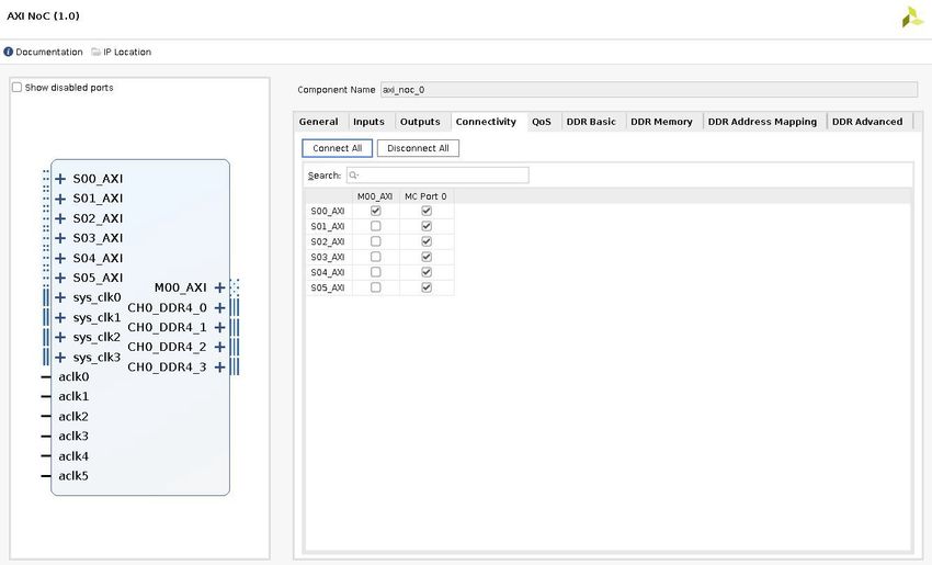
Chapter 1: Introduction

                                                                                      Chapter 1

Introduction
       The Xilinx® Versal™ platform Control, Interfaces and Processing System IP is the software
       interface around the Versal processing system. The Versal family consists of a system-on-chip
       (SoC) style integrated processing system (PS) and a programmable logic (PL) unit, NoC, and AI
       Engine providing an extensible and flexible SoC solution on a single die.

Features
       • Enable/Disable I/O peripherals (IOP)
       • Enable/Disable AXI Interfaces
       • Multiplexed I/O (MIO) configuration
       • Extended multiplexed I/Os (EMIO)
       • PL clocks, interrupts, and resets
       • Internal clocking (PMC/LPD/FPD)
       • Generation of system level configuration registers (SLCRs)
       • Enable/Disable PS to/from NoC Interface
       • PCIe® and CCIX configuration
       • SYSMON configuration
       • Debug configuration

PG352 (v3.0) June 16, 2021                                                              www.xilinx.com
                                                                      Send Feedback
CIPS IP Core                                                                                         4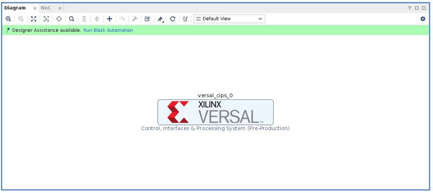
Chapter 1: Introduction

IP Facts
                                                        LogiCORE™ IP Facts Table
                                                                Core Specifics
        Supported Device Family                   Versal™ ACAP
        Supported User Interfaces                 AXI4, AXI4-Lite, AXI4-Stream, Native, and NoC
                                                             Provided with Core
        Design Files                              Verilog
        Example Design                            Refer block automation for DDR/CPM reference designs
        Test Bench                                N/A
        Constraints File                          N/A
        Simulation Model                          N/A
        Supported S/W Driver                      N/A
                                                             Tested Design Flows
        Design Entry                              Vivado®   Design Suite
        Simulation                                For supported simulators, see the Xilinx Design Tools: Release Notes Guide.
        Synthesis                                 Vivado Synthesis
                                                                   Support
        All Vivado IP Change Logs                 Master Vivado IP Change Logs: 72775
                                                            Xilinx Support web page
        Notes:
        1.   For a complete list of supported devices, see the Vivado® IP catalog.
        2.   For the supported versions of the tools, see the Xilinx Design Tools: Release Notes Guide.

PG352 (v3.0) June 16, 2021                                                                                       www.xilinx.com
                                                                                        Send Feedback
CIPS IP Core                                                                                                                  5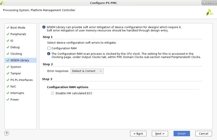
Chapter 2: Overview

                                                                                      Chapter 2

Overview

Navigating Content by Design Process
       Xilinx® documentation is organized around a set of standard design processes to help you find
       relevant content for your current development task. All Versal™ ACAP design process Design
       Hubs can be found on the Xilinx.com website. This document covers the following design
       processes:

       • Hardware, IP, and Platform Development: Creating the PL IP blocks for the hardware
         platform, creating PL kernels, functional simulation, and evaluating the Vivado® timing,
         resource use, and power closure. Also involves developing the hardware platform for system
         integration. Topics in this document that apply to this design process include:

          • I/O Peripheral and Flash Memory Controllers
          • Chapter 4: Design Flow Steps
          • Clocking

Core Overview
       The Control Interfaces and Processing System IP core instantiates, boots, and configures the
       processing system section of the Xilinx® Versal™ platform.

       CIPS 3.0 is architected as a hierarchical IP encapsulating two sub-IPs namely PS-PMC and CPM
       IPs. Designing for Versal™ always requires at the least the PMC involvement and therefore CIPS
       to be configured.

Licensing and Ordering
       This Xilinx® LogiCORE™ IP module is provided at no additional cost with the Xilinx Vivado®
       Design Suite under the terms of the Xilinx End User License.

PG352 (v3.0) June 16, 2021                                                               www.xilinx.com
                                                                     Send Feedback
CIPS IP Core                                                                                          6
Chapter 2: Overview
Note: To verify that you need a license, check the License column of the IP Catalog. Included means that a
license is included with the Vivado® Design Suite; Purchase means that you have to purchase a license to
use the core.
Information about other Xilinx® LogiCORE™ IP modules is available at the Xilinx Intellectual
Property page. For information about pricing and availability of other Xilinx LogiCORE IP modules
and tools, contact your local Xilinx sales representative.
PG352 (v3.0) June 16, 2021 www.xilinx.com
Send Feedback
CIPS IP Core 7Chapter 3: Product Specification
Chapter 3
Product Specification
The functional block diagram of the core is shown in the following figure.
Figure 1: Core Block Diagram
Programmable
Serial Logic
Transceivers
PCIe PCIe + DMA CCIX
CPM4
Security
Cortex-A72 Cortex-R5
Boot
Cortex-A72 Cortex-R5
& Config
Analog
APU RPU
Processing System
PMC
NoC
XPIO & Memory Controller
X23476-110320
I/O Peripheral and Flash Memory Controllers
The I/O Peripheral and Flash Memory Controllers include the following.
PG352 (v3.0) June 16, 2021 www.xilinx.com
Send Feedback
CIPS IP Core 8Chapter 3: Product Specification
• Quad Serial Peripheral Interface (QSPI) flash memory
• Octal Serial Peripheral Interface (OSPI) flash memory
• UART
• I2C
• Serial Peripheral Interface (SPI) flash memory
• SD/eMMC
• General purpose I/O (GPIO)
• Controller Area Network Flexible Data rates (CAN-FD)
• USB 2.0
• Gigabit Ethernet MAC (GEM)
Note: The interfaces for these I/O peripherals (IOPs) can be routed to MIO ports and the extended
multiplexed I/O (EMIO) interfaces as described in the Versal ACAP Technical Reference Manual (AM011).
• PMC domain peripheral
○ QSPI
○ OSPI
○ 2xSD/eMMC
○ I2C
○ SelectMAP (SMAP)
○ GPIOs
• Low power domain (LPD) peripherals available in PS:
○ 2 X Gigabit Ethernet
○ 1 X USB 2.0
○ 2 X SPI
○ 2 X CAN
○ 2 X I2C
○ 2 X UART
○ GPIOs
PG352 (v3.0) June 16, 2021 www.xilinx.com
Send Feedback
CIPS IP Core 9Chapter 4: Design Flow Steps
Chapter 4
Design Flow Steps
This section describes customizing and generating the core, constraining the core, and the
simulation, synthesis, and implementation steps that are specific to this IP core. More detailed
information about the standard Vivado® design flows and the IP integrator can be found in the
following Vivado Design Suite user guides:
• Vivado Design Suite User Guide: Designing IP Subsystems using IP Integrator (UG994)
• Vivado Design Suite User Guide: Designing with IP (UG896)
• Vivado Design Suite User Guide: Getting Started (UG910)
• Vivado Design Suite User Guide: Logic Simulation (UG900)
Customizing and Generating the Core
This section includes information about using Xilinx® tools to customize and generate the core in
the Vivado® Design Suite.
If you are customizing and generating the core in the Vivado IP integrator, see the Vivado Design
Suite User Guide: Designing IP Subsystems using IP Integrator (UG994) for detailed information. IP
integrator might auto-compute certain configuration values when validating or generating the
design. To check whether the values do change, see the description of the parameter in this
chapter. To view the parameter value, run the validate_bd_design command in the Tcl
console.
You can customize the IP for use in your design by specifying values for the various parameters
associated with the IP core using the following steps:
1. Select the IP from the IP catalog.
2. Double-click the selected IP or select the Customize IP command from the toolbar or right-
click menu.
For details, see the Vivado Design Suite User Guide: Designing with IP (UG896) and the Vivado
Design Suite User Guide: Getting Started (UG910).
Figures in this chapter are illustrations of the Vivado IDE. The layout depicted here might vary
from the current version.
PG352 (v3.0) June 16, 2021 www.xilinx.com
Send Feedback
CIPS IP Core 10Chapter 4: Design Flow Steps
CIPS IP Core Block Design
You can customize the Control Interfaces and Processing System IP core by clicking on the CIPS
IP. The block diagram on selecting the customization is shown in the following figure.
Figure 2: CIPS IP Core Block Design
PG352 (v3.0) June 16, 2021 www.xilinx.com
Send Feedback
CIPS IP Core 11Chapter 4: Design Flow Steps
Choosing a Design Flow
CIPS 3.0 is very flexible and can be configured in several different ways. CIPS IP enables
configuration of many operating parameters. There are two Design Flows available for
configuring these parameters. The two flows, based on the archetype of the two traditional user
persona, guide the user as per the predetermined presets. These two flows do not alter the
expert users complete freedom in the configuration order and options. They are in fact an
addition to help and guide the user.
Table 1: CIPS 3.0 Design Flows
Design Flow Description
PL Subsystem This flow configures only the vital components to use the
programmable logic (PL) domain of the Versal device. When
this flow is selected, only the Platform Management
Controller (PMC) is configured as it is necessary for
initialization of the Versal ACAP.
Note: All other device domains (For example, PS or CPM) are
disabled in this flow.
For example, if the design targets the programmable logic
exclusively and does not use any other domain, select this
flow.
Full System This flow configures all domains on the Versal ACAP. All
available domains on the device will be shown and available
for configuration.
Automation
The CIPS IP is supported by Vivado IP integrator optional assistance to the designer such as
Block and Board Automation. Block Automation provides an initial configuration and connects to
additional related IP blocks. Board Automation applies a specific configuration preset to CIPS IP
when a board part is chosen and has a preset. Therefore the CIPS IP settings are customized to
work with the targeted board.
In addition, other IPs may provide Connection Automation for additional peripheral/connectivity
to be connected to CIPS IP. Following are the automation limitations:
• Block, board, and connection automation are independent entities in the IP integrator. Using
multiple automations may cause conflicts.
• Connection Automation may not recognize hardened interfaces.
• Block Automation is not reentrant. It cannot be invoked twice unless the IP is removed from
IP integrator and added again.
PG352 (v3.0) June 16, 2021 www.xilinx.com
Send Feedback
CIPS IP Core 12Chapter 4: Design Flow Steps
Block Automation
Vivado® supports the Block Automation for Control, Interfaces and Processing System IP to aid
in integrating it into the larger design. After adding the CIPS IP to the block diagram, the block
automation banner pops up. Click Run Block Automation to open the block automation page.
Figure 3: Block Automation
Block automation supports the following options:
• Memory Controller: You can select x1/x2/x4 interleaved DDR4 or LPDDR DRAM controllers
and a new/existing NoC to be connected to the CIPS IP core.
• PL clocks/PL resets: You can select 0-4 PL clocks and 0-4 reset signals which are exposed to
PL.
• Design Flows: The two Design Flows are available and the selected flow is reflected in the
CIPS IP.
PG352 (v3.0) June 16, 2021 www.xilinx.com
Send Feedback
CIPS IP Core 13Chapter 4: Design Flow Steps
Figure 4: Run Block Automation
When you click OK, a validate ready design is provided with input requirements.
Note: The block automation banner disappears when CIPS IP instance configuration is updated/changed.
Thus, it must be the first configuration step if intended to be used.
Board Automation
When you create a Vivado® project targeting a board instead of a specific device, a board preset
may be available to initialize the CIPS IP core with board-specific settings.
After instantiating the CIPS IP in the block design, a green banner will appear indicating that
designer assistance is available. To access board automation, click Run Block Automation on this
banner.
To set the board preset, set Apply Board Preset to Yes in the Run Block Automation window.
IMPORTANT! If Apply Board Preset is set to No and block automation is run, the board preset will not be
applied. Ensure to manually enable peripherals on the Peripherals and I/O Configuration pages.
PG352 (v3.0) June 16, 2021 www.xilinx.com
Send Feedback
CIPS IP Core 14Chapter 4: Design Flow Steps
TIP: For ensuring flexibility, Vivado IP integrator provides a board tab available in the Data Windows Area,
where the various board presets are also available and can be dragged and dropped on the canvas.
Figure 5: Applying the Board Automation Using Block Automation
IMPORTANT! Using the Board window in IP integrator to drag the External Memory DDR4 or LPDDR4
interfaces onto the block design canvas does not applies the board preset and the connections to the
memory controllers in the NoC are not external. Execute the following procedure to apply board
automation to DDR4 or LPDDR4:
1. Open CIPS Block Automation window.
2. Select the desired Memory Controller Type and click Ok.
3. Verify that the selected memory controller is added to the block design canvas and the board
preset is applied.
PG352 (v3.0) June 16, 2021 www.xilinx.com
Send Feedback
CIPS IP Core 15Chapter 4: Design Flow Steps
CIPS Presets
CIPS 3.0 is enabled with default configurations for CIPS parameters referred as Presets. The
Presets facilitate design creation and block automation and enable users to quickly configure the
IP through GUI without digging into parameter details. Different Presets are available based on
the selected Design Flow. The default Presets represent the simplest and necessary options to
set up. The options are based on traditional, most encountered use-cases, and on device minimal
boot and run-time requirements.
There are two Design Flows available namely PL Subsystem and Full System. On the basis of the
Design Flow selected, the default Presets configurations are enabled into selected parameter.
TIP: It allows changing Presets value by user at later stage in PS PMC and CPM windows.
Clicking Apply Configuration in Presets enables user to import presets through Presets Tcl
file.
Enabled Presets provides a summary of selected parameters for configuration.
Having Presets in CIPS ensures minimum amount of steps required to achieve the configuration
needed for their flow.
• PL Subsystem: It stands for PMC + PL where no Processing System is used. It is aimed at
traditional FPGA designers, with no to limited interest in the Processing system. This is why
some presets are grayed out in PL Subsystem but enabled in Full System Configuration.
• Full System: It stands for PS + PMC + CPM + PL and is aimed at the Embedded designer with
a definitive interest in PS and/or CPM configuration and interaction with DDR and potential
interaction with PL. The advanced user can select the Full System Design Flow and potentially
some presets, but can skip the presets. Click the Next button to access the PS PMC and CPM
IPs within CIPS to configure them. It is aimed at an advanced user with knowledge above what
is expected as standard.
The presets configurations applied are then visible within the PS PMC IP by clicking Next and
accessing the detailed settings within the PS PMC Sub-IP.
Note: The Presets set to Custom do not apply any configuration.
The PS-PMC sub-IP exposes all the details and options hidden in the Presets. Presets can be
used as a basis to then tune the configuration further. IO Pins allocations and conflicts resolution
are easily achieved through one and only one panel. The IO panel which provides a general view
of the interfaces currently selected to leverage MIOs and their respective MIO pins layout. Any
MIO conflict is highlighted in red.
PG352 (v3.0) June 16, 2021 www.xilinx.com
Send Feedback
CIPS IP Core 16Chapter 4: Design Flow Steps
Figure 6: Presets in CIPS 3.0
The following are the Presets available in CIPS 3.0 module:
• Board Interface Configures default boot mode and the default set of peripherals and clocks
found on the selected board part when ps pmc fixed io is selected.
TIP: This is only visible when Full System design flow is selected.
• Boot Configuration Selects boot configuration from Master, Slave, JTAG, or Custom.
• Clock Settings Sets the system reference clock frequency REF_CLK to 33.33 MHz.
• Connectivity to MC via NoC Enables the dedicated connectivity that can be used to connect
to a NoC instance with a memory controller.
• IO Peripherals
TIP: This is not applicable when PL Subsystem is selected in the Design Flow.
PG352 (v3.0) June 16, 2021 www.xilinx.com
Send Feedback
CIPS IP Core 17Chapter 4: Design Flow Steps
As JTAG is always available on Versal, the Debug preset set to custom or JTAG has no effect
and defaults to JTAG support via DAP.
• Debug Selects one of the debug option from JTAG, HIGH Speed Debug Port (HSDP), or
Custom.
• Device Integrity Enables you to monitor and respond to the system operating conditions and
exceptional events.
• PS PL Connectivity Selects Single FPD and Master/Slave LPD clock.
TIP: This is not applicable when PL Subsystem is selected in the Design Flow.
CPM
The Control, Interfaces and Processing System IP core is also used to configure the PCIe®
module. There are direct interfaces to the CPM, which includes a complete subsystem for PCIe.
Certain devices do not offer CPM, while others which do offers either a CPM4 or a CPM5
version of this block. It is no longer clearly defined by which Versal series due to derived devices.
For example, some higher-end Premium provides CPM5, and AI Edge provides both CPM4 and
CPM5.
Note: For 2021.1, only the Full System (PS + PMC + CPM + PL) flow supports PCIe® configurations in the
CPM block.
PG352 (v3.0) June 16, 2021 www.xilinx.com
Send Feedback
CIPS IP Core 18Chapter 4: Design Flow Steps
Figure 7: CPM4 Basic Configuration
PG352 (v3.0) June 16, 2021 www.xilinx.com
Send Feedback
CIPS IP Core 19Chapter 4: Design Flow Steps
Figure 8: CPM5 Basic Configuration
Note: For more information on CPM module, see Versal ACAP CPM Mode for PCI Express Product Guide
(PG346), Versal ACAP CPM DMA and Bridge Mode for PCI Express Product Guide (PG347), and Versal ACAP
CPM CCIX Architecture Manual (AM016).
Device Integrity
The Device integrity feature enable users to monitor and respond to the system operating
conditions and exceptional events. Many of these features are broadly applicable to many
designs, while others are provided in support of meeting stringent reliability, security, and safety
requirements. Device integrity has three modules namely, SYSMON, XilSEM Library, and Tamper
configurations as described in subsequent sections.
PG352 (v3.0) June 16, 2021 www.xilinx.com
Send Feedback
CIPS IP Core 20Chapter 4: Design Flow Steps
System Monitor
The System Monitor (SYSMON) enables monitoring of the physical environment both within the
Versal™ ACAP itself and also within the wider system using the external inputs. It is used to
ensure that both the Versal ACAP and the overall system operate in a safe, secure, and reliable
way. The SYSMON provides the customer with a digital measure of the temperature and applied
voltage supplies as well as off-chip voltage measurements within the broader system context.
Off-chip, its main uses are for board level monitoring of supply voltages/currents.
The Control, Interfaces and Processing System IP core can enable the following measurements:
• On-chip Supply Monitor
• Temperature Measurements
• External Supply Measurements
The Basic Configuration tab has Default and Custom options, as shown in the following figure.
PG352 (v3.0) June 16, 2021 www.xilinx.com
Send Feedback
CIPS IP Core 21Chapter 4: Design Flow Steps
Figure 9: SYSMON Basic Configuration
The default window has different preset options to provide a common starting point for typical
SYSMON usage. Each measurement has associated threshold levels which control alarm
assertion. The alarms are enabled by default. For external access to SYSMON measurements,
I2C, and PMBus interfaces are supported.
The default window also provides the option for setting the voltage averaging levels of 2, 4, 8,
and 16. The MIO pin allocation can be modified through the IO panel. Any MIO conflict is
highlighted with icon.
On-Chip Supply Monitor
The On-chip supply monitor tab supports different types of voltage measurements including
customer supply voltages and customer dedicated pad voltages.
PG352 (v3.0) June 16, 2021 www.xilinx.com
Send Feedback
CIPS IP Core 22Chapter 4: Design Flow Steps
The On Chip Supply Monitor configuration is shown in the following figure.
Figure 10: On Chip Supply Monitor
The CIPS IP core allows you to enable averaging, define the ADC Mode (unipolar/bipolar), and
enable alarms with user-defined upper and lower thresholds.
Temperature Measurements
The Temperature configuration tab configures device temperature monitoring options, including
over-temperature shutdown. Alarms are all specified in window mode, where the alarm is
asserted above the upper threshold or blow the lower threshold. You can configure the lower and
upper temperature value based on the design requirements.
PG352 (v3.0) June 16, 2021 www.xilinx.com
Send Feedback
CIPS IP Core 23Chapter 4: Design Flow Steps
Figure 11: Temperature Configuration
External Supply Measurements
The Control, Interfaces and Processing System IP core allows up to 16 pins to be selected for
external supply measurements. All AUXIOs should be assigned to the same bank.
For example, if AUX_IO_P is LPD Bank MIO0 (VCCO_502 rail), then AUX_IO_N should be
assigned from LPD MIO Bank MIO (VCCO_502 rail).
The AUXIOs supports PMC MIOs, LPD MIOs, and HDIOs. But PMC and LPD MIOs may have
conflict based on PS-PMC IO Configuration page. To resolve the conflict, use other free available
IOs.
The External Supply monitor configuration tab is shown in the following figure:
PG352 (v3.0) June 16, 2021 www.xilinx.com
Send Feedback
CIPS IP Core 24Chapter 4: Design Flow Steps
Figure 12: SYSMON External Supply Monitor
XilSEM Library Configuration
The Xilinx Soft Error Mitigation (XilSEM) library provides a pre-configured and pre-verified
solution to detect and optionally correct soft errors in Configuration Memory of Versal ACAPs.
The fundamental feature of the XilSEM Library can be enabled in CIPS. This features soft error
mitigation of Configuration RAM through a scan-based process automated by integrated logic. It
is managed by the XilSEM Library which reads back Configuration RAM and uses ECC and CRC
to detect and correct soft errors. If this feature is enabled in CIPS, the default behavior is to begin
operation automatically after boot, calculate golden checkrooms using hardware resources, and
then enable the process for error detection and correction. These options can also be accessed
through properties applied to the design. The following figure shows the fundamental feature
accessible through the XilSEM Library configuration section of the CIPS GUI.
PG352 (v3.0) June 16, 2021 www.xilinx.com
Send Feedback
CIPS IP Core 25Chapter 4: Design Flow Steps
Figure 13: XilSEM Library Configuration
Advanced features of the XilSEM Library can be accessed through properties applied to the
design. The XilSEM Library provides an optional feature for the soft error mitigation of NPI
Registers, provided the supplemental hardware resources required for this feature are accessible.
This feature is a scan-based process automated by integrated logic and managed by the XilSEM
Library, which reads back NPI Registers and uses SHA to detect errors. For more information, see
OS and Libraries Document Collection (UG643).
Tamper Events/Response Configuration
Tamper events are interrupts from a tamper monitoring function and user can select different
responses to each tamper events.
PG352 (v3.0) June 16, 2021 www.xilinx.com
Send Feedback
CIPS IP Core 26Chapter 4: Design Flow Steps
Figure 14: Tamper Response System
Tamper monitoring system in CIPS generates interrupts as an when it detects below events.
• Supply Glitch: Whenever there is a glitch in power supply happens, then this event will get
generated. Glitching the power supply (low or high) can cause insecurely designed state
machines to skip states. Glitches are injected at various points in time and vary in pulse
widths.
• Temperature Deviation: When device temperature goes out of specification (high or low) then
this event will be generated. This is commonly done in conjunction with a voltage attack. Both
low and high temperature cause race conditions that can trip just about any type of circuity.
• Debug (JTAG) toggle detect: Debug interfaces attack the Silicon devices, most frequently this
is the JTAG port but with the growing complexity of devices more advanced debug interfaces
are becoming more prominent. This event would be generated when there is a toggle in debug
interfaces.
• Custom User (External MIO) event: This event is generated when Tamper monitoring system
detects any interrupt (active-High) on external MIO.
• Tamper Register event: When you directly trigger the tamper system by writing to its specific
register, then this event would be generated.
CIPS has different responses to each of the above mentioned tamper events, which are described
below.
• BBRAM Zeroization: When a tamper event is detected, it is required that the you can
immediately erase the key stored in BBRAM. However, in high grade crypto applications, it is
not sufficient to simply delete the key when done or when a tamper event is detected. It is
required to be zeroized (erase + verify). CIPS provides this response for all the tamper events.
PG352 (v3.0) June 16, 2021 www.xilinx.com
Send Feedback
CIPS IP Core 27Chapter 4: Design Flow Steps
• Secure Lockdown: Upon detection of a tamper event, you want the system to go into some
form of lockdown state. CIPS provides lockdown response for all the tamper events.
• Secure Lockdown (With IO Tristate): Some systems require a more severe response to a
tamper event and even secure lockdown is not enough. It such cases it is necessary to also
tristate all IO to the device. This makes it impossible for the adversary to gain any level of
access to the device after a tamper event. CIPS provides lockdown with IO Tristate response
for all the tamper events.
• System Reset: You may want to only Reset the system, upon receiving the tamper event. CIPS
provides System Reset response for all the tamper events.
• System Interrupt: You may only want to know that the tamper event is occurred. Tamper
response system generates an interrupt to system, upon receiving any tamper event.
You can select BBRAM Zeroization or Secure Lockdown or Secure Lockdown (With IO Tristate) or
System Reset or System Interrupt for each Tamper Event as response in PCW.
PG352 (v3.0) June 16, 2021 www.xilinx.com
Send Feedback
CIPS IP Core 28Chapter 4: Design Flow Steps
Figure 15: Tamper Events/Response Configuration
PS-NoC Interfaces
The PS-NoC Interfaces tab enables memory-mapped connectivity from the Control, Interfaces
and Processing System processors to other Versal™ device resources such as DDR, AI Engine,
and PL.
The following table lists the NoC interfaces from which you can select in the customization core:
PG352 (v3.0) June 16, 2021 www.xilinx.com
Send Feedback
CIPS IP Core 29Chapter 4: Design Flow Steps
Table 2: List of NoC Interfaces
Interface Name Size Notes
4 NoC Master Ports 128-bit channels PS-CCI → NoC channels
2 NoC Master Ports 128-bit channels PS-NCI → NoC channels
1 NoC Master Ports 128-bit channels PS-LPD (RPU) → NoC channels
1 NoC Master Ports 128-bit channels PMC/Debug → NoC channels(via LPD)
2 NoC Master Ports 128-bit channels CPM4/5 (PCIe/CCIX) → NoC channels (via LPD)
4 NoC Slave Ports 128-bit channels NoC → PS channels (2 go to CCI, 2 go to NCI)
1 NoC Slave Ports 128-bit channels NoC → PS-LPD/PMC channels
1 NoC Slave Ports 128-bit channels NoC → PCIe/CCIX/CPM4/5 channels (via LPD)
The CIPS IP core for the NoC interface selection is shown below:
Figure 16: PS-NoC Interfaces
PG352 (v3.0) June 16, 2021 www.xilinx.com
Send Feedback
CIPS IP Core 30Chapter 4: Design Flow Steps
The following are a few recommendations on the usage of PS-NoC ports.
• If any design has AI Engine then you must enable PMC NoC port for AI Engine configuration.
• By default, the 32-bit RPU is unable to access or control the AI Engine at its >32-bit address.
This access can be enabled by remapping the entire LPD_AXI_NOC_0 address range of the
upper 1GB of DDR LOW0 region (0x40000000 to 0x7FFFFFFF) to the AI Engine for all LPD
masters with the Tcl command (assuming axi_noc_0 is the NoC instance name, and
LPD_AXI_NOC is connected to S00_AXI, and the AI Engine IP is connected to M00_AXI):
set_property CONFIG.REMAPS {M00_AXI {{0x4000_0000 0x200_0000_0000 1G}
[get_bd_intf_pins /axi_noc_0/S00_AXI]}}
If any LPD masters such as LPDMA, GEM, or USB DMA still want to access the full DDR at
this range, these masters transactions must be routed through the FPD.
Note: Following is the Tcl command to enable the route through FPD support for LPD Masters:
set_property -dict [list CONFIG.PS_PMC_CONFIG
{PMC_SD0_ROUTE_THROUGH_FPD 1
PMC_SD1_ROUTE_THROUGH_FPD 1
PMC_OSPI_ROUTE_THROUGH_FPD 1
PMC_QSPI_ROUTE_THROUGH_FPD 1
PS_USB_ROUTE_THROUGH_FPD 1
PS_GEM0_ROUTE_THROUGH_FPD 1
PS_GEM1_ROUTE_THROUGH_FPD 1
PS_LPDMA0_ROUTE_THROUGH_FPD 1
PS_LPDMA1_ROUTE_THROUGH_FPD 1
PS_LPDMA2_ROUTE_THROUGH_FPD 1
PS_LPDMA3_ROUTE_THROUGH_FPD 1
PS_LPDMA4_ROUTE_THROUGH_FPD 1
PS_LPDMA5_ROUTE_THROUGH_FPD 1
PS_LPDMA6_ROUTE_THROUGH_FPD 1
PS_LPDMA7_ROUTE_THROUGH_FPD 1}]
[get_bd_cells versal_cips_0]
• All 4 PS to NoC CCI ports must connect to the NoC.
NoC Interfaces
The following is the list of interfaces between PS/PMC and NoC. You can select these in the NoC
interfaces section to communicate with the DDR/PL/AIE.
• Coherent (CCI) master ports: The CIPS IP core has four coherent master ports
(FPD_CCI_NOC_0,1,2,3) connected from PS-CCI to NoC. CCI drives these ports in
interleaving mode (2 ports and 4 ports), so you must connect all 4 ports to NoC to access any
slave. The CIPS core masters A72/R5/PMC/DMA can make use of these ports. Also, PL
masters that are connected to CIPS on CCI slave ports can access these ports.
• Non-Coherent (NCI) master ports: The CIPS core has two non-Coherent master ports
(FPD_AXI_NOC_0,1). Only PL masters which are connected to NCI slave ports of the CIPS
core can access these ports.
PG352 (v3.0) June 16, 2021 www.xilinx.com
Send Feedback
CIPS IP Core 31Chapter 4: Design Flow Steps
TIP: Coherency is NOT enabled by default at boot on the CCI AXI-Lite ports.
• LPD (RPU) master port: There is one master port from LPD (NOC_LPD_AXI_0) to NoC. LPD
masters RPU/DMA can make use of this master port to access slaves.
• PMC master port: The CIPS core has one master port (PMC_NOC_AXI_0) from PMC domain
to NoC. This port is used by PMC for debug/boot.
• CPM4/5 master ports: Two master ports (IF_PS_NOC_PCIE_0,1) are exposed from the CIPS
core. One is connected to PCIe0 controller and the other is to CCIX module. CPM4/5 can
access DDR/PL/AIE regions using these ports. You can select connected ports in the CPM4/5
Configuration page.
• Coherent (CCI) Slave ports: The CIPS core has two coherent slave ports (NOC_FPD_CCI_0,1).
Masters connected to these ports can achieve coherency and virtualization. Masters
connected to these ports can access DDR, PL slaves which are connected to CIPS via CCI
ports. Also PL masters have access to CIPS internal memory regions.
• Non-Coherent (NCI) Slave ports: The CIPS core has two non-coherent slave ports
(NOC_FPD_AXI_0,1). Masters connected to these ports can achieve only virtualization. PL
masters connected to these ports can access DDR, PL slaves which are connected to CIPS via
NCI ports. Also PL masters have access to CIPS internal memory regions.
• PMC/LPD Slave port: There is one slave port (NOC_PMC_AXI_0) to LPD/PMC region. PL
masters connected to this port will get access to these regions.
• CPM4/5 Slave port: The CIPS core has one NoC slave port (IF_NOC_PS_PCIE_0) connected
to CPM4/5 module. External masters can connect to this port to configure the CPM4/5. You
can select this port in the CPM4/5 Configuration page.
Figure 16: PS-NoC Interfaces shows different NoC master/slave port options to enable these
ports.
The following table shows the addresses you can assign to DDR/AI Engine/PL slaves which are
connected to CIPS master NoC ports. For more information on NoC address ranges and
configuration, see Versal ACAP Programmable Network on Chip and Integrated Memory Controller
LogiCORE IP Product Guide (PG313).
PG352 (v3.0) June 16, 2021 www.xilinx.com
Send Feedback
CIPS IP Core 32Chapter 4: Design Flow Steps
Table 3: NoC Region Address
Slave Region Start Address Size
Low0 0x0 2 GB
Low1 0x800000000 32 GB
Low2 0xC000000000 256 GB
DDR Low3 0x10000000000 734 GB
CH1 0x50000000000 1 TB
CH2 0x60000000000 1 TB
CH3 0x70000000000 1 TB
PLNOC2 TB 0x20100000000 2044 GB
PL
PLNOC8 TB 0x80000000000 8 TB
AI Engine AIE_0 0x20000000000 4 TB
The following figures describe CIPS + DDR + PL slave connections on NoC:
Figure 17: CIPS NoC
PG352 (v3.0) June 16, 2021 www.xilinx.com
Send Feedback
CIPS IP Core 33Chapter 4: Design Flow Steps
Figure 18: NoC General Configuration
Figure 19: NoC Slave Ports Configuration
PG352 (v3.0) June 16, 2021 www.xilinx.com
Send Feedback
CIPS IP Core 34Chapter 4: Design Flow Steps
Figure 20: NoC Master Ports Configuration
Figure 21: NoC Connectivity Configuration
PG352 (v3.0) June 16, 2021 www.xilinx.com
Send Feedback
CIPS IP Core 35Chapter 4: Design Flow Steps
Clocking Configuration
This page enables you to configure the peripheral clocks, PL clocks, DDR memory, AI Engine, and
CPU clocks. For an overview of the reference clocks used to generate the available clocks see the
Clock Distribution Diagram in the Versal ACAP Technical Reference Manual (AM011).
Clocking
There are three clock groups as follows.
• Main Clock Group (MCG). This group has the following PLLs:
○ RPU PLL
○ APU PLL
○ PMC PLL
○ NoC PLL
○ CPM4/5 PLL
• RTC Clock Group (RCG). This is a real-time clock, and a dedicated internal clock for RTC. A
clock divider is not required for this clock.
• Interface Clock Group (ICG). This group has clocks that are provided externally, like the clocks
from the physical-side interface (PHY) and PL.
Note: PL side peripherals can be operated through a PL clock (PL_REF_CLK).
Input Clocks
Following are the two input clocks.
• Input Reference frequency : This is the frequency of the clock that is coming from the on-
board clock source (REF_CLK).
• Peripheral Reference frequency: This section lists the clock pins and the input frequencies for
the peripherals where the clock is driven by MIO pins.
PG352 (v3.0) June 16, 2021 www.xilinx.com
Send Feedback
CIPS IP Core 36Chapter 4: Design Flow Steps
Figure 22: Input Clocks Configuration
Output Clocks
This section displays the default/user selected peripheral clocks which are allowed to update the
frequency. Also output clocks hold different domain PLLs.
PLLs in the PS and PMC are:
• APLL: APU PLL which is in FPD domain
• NPLL: NoC PLL which is in PMC domain
• RPLL: RPU PLL which is in LPD domain
• PPLL: PMC PLL which is in PMC domain
PG352 (v3.0) June 16, 2021 www.xilinx.com
Send Feedback
CIPS IP Core 37Chapter 4: Design Flow Steps
In the default mode (when the manual mode is turned off), the core automatically chooses the
source PLLs and calculates the M (Multiplier) and D (Divisor) values, to ensure that the tool
meets the requested frequency to the nearest possible value. The core might not achieve all the
requested values, since each PLL caters to multiple peripherals. An internal algorithm creates the
best possible solution based on the following conditions.
The algorithm chooses source PLL on its own and the rule is the PMC domain PPLL, NPLL can be
used to source in LPD and FPD. The LPD domain RPU PLL can be used to source in and FPD,
vice-versa is possible only by setting cross domain PLL parameter.
• When Ethernet is enabled, the core tries to give the precedence to the solution which has the
Ethernet frequency of 125 MHz. In manual mode divisors should be made in order to obtain
either of 125/25/2.5 MHz.
• When Ethernet is enabled and if there are multiple clocking solutions with the identical
Ethernet frequency of 125 MHz, then the tool will take the precedence of the solution that
will have the least possible total error (sum of requested frequencies-sum of actual
frequencies) value of various peripherals.
• The tool will also take the precedence of the solution with least possible total error value of
various peripherals even when the Ethernet is disabled.
• The tool will generate CAN clocks within 0.25 % tolerance and GEM clocks with +/- 100 ppm
tolerance. If the tool unable to derive these with set of input clocks then it generates a DRC.
• Tool will generate SDIO ref clock and SD DLL clocks as mentioned below.
1. In auto mode fixed 200 MHz for SDIO0/1 and 1200 MHz for SD DLL.
2. In manual mode DRC is provided if you are not using the same PLL for SD DLL and
SDIO0/1 ref clock.
3. In manual mode DRC is provided if SD DLL ref clock is not = 6 times SDIO0/1 ref clock.
PG352 (v3.0) June 16, 2021 www.xilinx.com
Send Feedback
CIPS IP Core 38Chapter 4: Design Flow Steps
Figure 23: Output Clocks
Enable Manual Clocking Mode
When you select this mode, different options are displayed. You can directly input the Source
PLL, M and D values for various PLLs as well as individual peripheral clock divisor values enabling
finer control. In Manual clocking mode, the default divisor values are given for input Ref clock
frequency of 33.33 MHz. If you move to the manual mode with different ref clock frequency,
then you will encounter DRC’s for divisor values which user need to resolve manually.
PMC Power Domain Clocks
• Processor/Memory Clocks: Clock configuration for the HSM0, which is source for AIE PLL.
HSM1 which is source for DDR PLL.
• Peripherals/IO Clocks: Clock configuration for boot devices like OSPI, SD/eMMC and clocks
for NPI, NoC.
• Interconnect and Switch Clocks: Clock configuration for interconnects and switches in PMC
domain.
PG352 (v3.0) June 16, 2021 www.xilinx.com
Send Feedback
CIPS IP Core 39Chapter 4: Design Flow Steps
Low Power Domain Clocks
• Processor/Memory Clocks: Clock configuration for the CPU_R5 Processor.
• Peripherals/IO Clocks: Clock configuration for low-speed peripheral devices.
• Interconnect and Switch Clocks: Clock configuration for interconnects and switches in LPD
domain.
• System Debug Clocks: Clock configuration for debug modules DBG_LPD, DBG_TSTMP.
Full Power Domain Clocks
• Processor/Memory Clocks : Clock configuration for APU, GPU, and DDR
• System Debug Clocks : Clock configuration for debug modules: DBG_FPD
• Interconnect and Switch Clocks : Clock configuration for interconnects and switches in FPD
domain
PL Clocks
The Versal Control, Interfaces and Processing System provides four clocks to the PL. Versal CIPS
IP core enables the configuration of these clocks to be used in the PL. The Versal CIPS core
inserts a BUFG for each of the PL clocks. Also, PCW provide option to select IRO clock to enable
and connect to PL peripherals.
You can use PMC domain PLL's in FPD and LPD but the reverse is not allowed because only
forward path clocking is followed in CIPS.
Table 4: Output Clocks and their Descriptions
Output Clock Description
Source This is the source PLL for the corresponding peripheral
Requested Freq (MHz) This is the input frequency given to the corresponding peripheral
Divisor 0 Denotes the 6-bit programmable Divisor
Actual Freq (MHz) This is the actual frequency calculated by the Processor Configuration. The
clocking algorithm works with multiple factors, peripherals, PLLs, and priorities.
Therefore, in certain cases, the actual frequency might be different than the
requested frequency.
Range (MHz) This is the minimum/maximum range of the frequency that the corresponding
peripheral can work with. In this mode, you must configure the M and D values
to achieve the desired frequency. When this mode is enabled, the values
requested through the output mode will be overwritten.
Note: In order to modify the clock frequencies/divisors, the corresponding clock must be enabled.
PG352 (v3.0) June 16, 2021 www.xilinx.com
Send Feedback
CIPS IP Core 40Chapter 4: Design Flow Steps
PLL Options for Output Clocks
There are four PLLs available in the Versal™ PS and PMC that are spread across the 3 domains,
PMC, LPD and FPD. There are two PLLs namely PPLL and NPLL in the PMC domain while the
RPLL in the LPD domain and APLL in FPD domain. The Control, Interfaces and Processing
System IP core provides an option to make use of the cross domain PLLs to be used to source the
cross-over peripheral. This gives additional options to select from a pool of all PLLs.
Table 5: PLL Options
PLL Option Description
Name One of the four PLLs available in APLL, RPLL, PPLL, and NPLL.
Source This is the source PLL for the corresponding peripheral.
Multiplier (FBDIV) Denotes the 6-bit Integer value which will be used as multiplier in calculating the
respective PLL output frequency.
CLKOUTDIV Enable the divide by 2/4/8 function inside the PLL. The output of this will be the
actual output frequency of respective PLL.
PLL output (MHz) Final output frequency of the respective PLL.
Cross domain Paths Denotes the cross-domain name as APLL_TO_LPD for FPD PLLs, NPLL/
PPLL_TO_FPD for PMC PLL’s and RPLL_TO_FPD for LPD PLLs.
Divisors Denotes the 6-bit integer value. This value will be used as divisor in calculating
the cross-domain output frequency for respective PLL.
Output frequency (MHz) PLL output frequency for cross domain.
In the Auto mode, you may not get the actual frequency that is requested due to the load of
different clocks on the same source PLL. After instantiating the CIPS IP core, some clocks are
enabled by default as per the clocking sheet of the respective part.
I/O Configuration
The I/O Configuration page reflects the peripherals and their I/O connectivity. You can assign
attributes for the signals. The I/O peripherals are categorized into two domains PMC and PS.
There are total 78 MIOs, 52 in PMC region (PMC MIO Bank0 and PMC MIO Bank1) and 26 in PS
region (LPD MIO Bank). Each IO can be assigned to any peripheral based on rules.
Alternatively, the same pins from each peripheral can be routed to EMIO signals which brings the
signal to PL section of the device for further processing. For more information on the MIO and
EMIO, refer to the Multiplexed I/O in the Versal ACAP Technical Reference Manual (AM011). MIOs
available for peripheral pinouts are divided into three Banks: PMC MIO Bank0 (MIO 0-25), PMC
MIO Bank1 (MIO 26-51), and LPD MIO Bank (MIO 52-77). Each bank has a common I/O Voltage
Standard for all its MIOs and the default value for this is LVCMOS1.8 and there are two more
options of LVCMOS2.5 and LVCMOS3.3 I/O voltage standard.
PG352 (v3.0) June 16, 2021 www.xilinx.com
Send Feedback
CIPS IP Core 41Chapter 4: Design Flow Steps
You can select the peripherals, GPIOs, and tamper signals in core to make use of the MIOs. DRC
messages will be shown to alert if any MIO conflict occurs between multiple peripherals. Each
peripheral has different set of supported MIO where you can play between these to avoid the
DRC of MIO conflict between peripherals. Also, you have EMIO option for each peripheral, this
option also can be selected to resolve MIO conflicts.
Upon enabling the peripheral in I/O configuration page, you will able set the respective
peripheral frequency in Clock Configuration.
For each MIO, there are set of pin pad attributes where user can set these attributes in the core
by clicking on respective MIO.
• Drive: MIO pin pad attribute Drive Strength in mA, used to select the drive strength. Possible
values are 2, 4, 8, and 12.
• Slew: MIO pin pad attribute Speed, specifies whether the device is fast or slow depending on
the slew rate.
• Pull: MIO pin pad attribute Pull Type, used to enable/disable a device along with pull-up or
pull-down.
• Schmitt: MIO pin pad attribute I/O type, select CMOS or Schmitt as the input I/O voltage
type.
• Direction: MIO pin pad attribute Direction, the direction can be fixed for certain signals.
The following diagram shows the PS/PMC MIO banks and MIO pad attributes settings.
PG352 (v3.0) June 16, 2021 www.xilinx.com
Send Feedback
CIPS IP Core 42Chapter 4: Design Flow Steps
Figure 24: I/O Configuration
MIO I/O Reservation
The MIO Reservation feature allows you to select the unused/unassigned MIO’s as GPIO/AUX-
IO. To select these, you are required to click the MIO PIN view button from the toolbar and
then select GPIO/AUX-IO options in the External Usage column for the respected MIO. If any
MIO is allocated to a peripheral then that MIO cannot be set as GPIO/AUX-IO, so its External
Usage drop down is disabled.
If the MIO usage is GPIO, then you can set its output data as active-High or active-Low and
direction as In or Out. After boot, this value will be driven on IO when it is set in Out direction. If
the MIO usage is AUX-IO, only then you can set direction as In/Out.
PG352 (v3.0) June 16, 2021 www.xilinx.com
Send Feedback
CIPS IP Core 43Chapter 4: Design Flow Steps
Figure 25: MIO I/O Reservation Settings
The IO-Configuration page also allows you to select 64 GPIO-EMIO pins in PMC domain and 32
GPIO-EMIO pins in PS domain. Upon enabling this, these pins will be exposed to the PL region.
MIO Ports
In the Versal™ design tools, Control, Interfaces and Processing System IP core is used to
configure the core Multi-Use IO (MIO) ports. There are up to 78 MIO ports available from the
CIPS IP core. This core allows you to choose the different peripheral ports to be connected to the
MIO ports.
Extended MIO Ports
Since there are only up to 78 MIO ports available, many peripheral I/O ports beyond these can
still be routed to the programmable logic through the Extended MIO (EMIO) interface.
Alternative routing for IOP interfaces through programmable logic enables you to take full
advantage of the IOP available in the CIPS IP core. The EMIO for I2C, SPI flash memory, Gigabit
Ethernet Management Data Input/Output (MDIO), SD/eMMC, GPIO 3-state enable signals are
inverted in the Versal CIPS IP core. The Versal CIPS IP core allows you to select GPIO up to 96
signals. The Versal CIPS IP core has control logic to adjust user-selected width to flow into CIPS
IP core.
PG352 (v3.0) June 16, 2021 www.xilinx.com
Send Feedback
CIPS IP Core 44Chapter 4: Design Flow Steps
PL-PS Configuration
The PL-PS Configuration page controls which interfaces are exposed on the block to the PL.
Figure 26: PL-PS Interfaces illustrates the PL-PS interfaces in Control, Interfaces and Processing
System IP core, where we have two GP master ports to PL and three GP slave ports from the PL.
Adding to that we have one ACE and one ACP ports from the PL. All of them have a maximum
data width of 128 bits.
AXI4 I/O Compliant Interfaces
Following are the AMBA® AXI4 compliant interfaces:
• Two PS General Purpose Master interfaces user configurable as 32, 64, and 128 bits in width.
The default width is 128.
• Three PL General Purpose Master interfaces user configurable as 32, 64, and 128 bits in
width. The default width is 128.
• A 128-bit PL Master AXI coherency extension (ACE) interface for coherent I/O to CCI module.
• A 128-bit PL Master ACP interface to support L2 cache allocation from PL masters. Limited to
64-byte cache line transfers.
Figure 26: PL-PS Interfaces
PG352 (v3.0) June 16, 2021 www.xilinx.com
Send Feedback
CIPS IP Core 45Chapter 4: Design Flow Steps
The CIPS IP core has two master ports to PL and three slave ports from the PL. Adding to that
we have one ACE and one ACP port from the PL. All of them have a maximum default data width
of 128 bits and can be selectable as 32-bit, 64-bit, or 128-bit.
The following are the details of the PL interfaces:
• ACE: A full ACE slave port (S_ACE_FPD) allowing 2-way coherency between the APU and a
PL master. The PL masters can also snoop APU caches via APU ACP port.
• ACP: A 1-way coherency slave port (S_ACP_FPD) directly connected the APU, allowing
external PL master to allocate memory directly into the L2 cache.
• AXI Slave Ports:
• Two AXI slave ports (S_AXI_FPD, S_AXI_GP2/S_CCI_FPD) allowing PL masters direct
access to the PS not via the NoC
○ PL Masters connected to S_AXI_FPD have access to the following:
- Complete PS subsystem
- DDR, PL slaves which are connected to CIPS NCI port
- PL slaves which are connected to M_AXI_FPD port
○ PL Masters connected to GP2 port have access to the following:
- Complete PS subsystem
- DDR, PL slaves which are connected to CIPS CCI port
- PL slaves which are connected to M_AXI_FPD port
The GP2 port can be used as AXI4 port or ACE_LITE port. In GUI if GP2 port is enabled,
then it acts as AXI4 port. If you set GP2 port in GUI and below user parameter in tcl
prompt then it acts as ACE_LITE port.
set_property -dict [list CONFIG.PS_PMC_CONFIG {PS_USE_ACE_LITE 1}]
[get_bd_cells /versal_cips_0]
• One direct AXI slave port ( S_AXI_LPD) allowing PL masters access to LPD independent of
FPD power state. PL masters connected to this masters has access to complete LPD
subsystem.
• AXI Mater Ports:
• One AXI master port (M_AXI_FPD) allowing PS masters and PL masters (which are
connected to CIPS S_AXI_FPD, GP2 and CIPS NOC slave ports) access to PL slaves.
• One direct AXI master port (M_AXI_LPD) allowing LPD masters access to PL slaves
independent of FPD power state
PG352 (v3.0) June 16, 2021 www.xilinx.com
Send Feedback
CIPS IP Core 46Chapter 4: Design Flow Steps
The Versal CIPS IP core provides four resets to the PL. It enables the configuration of these
resets to be used in the PL, which are asynchronous to any clock. These resets will be de-
asserted after the PL configuration process.
Using this page, you can also configure the PS to PL interface signals related to Ethernet (FIFO,
PTP and TSU) and LPD_DMA flow control support.
Masters have to choose different addresses for the connected PL slaves. Based on which AXI
port the slaves are connected to CIPS, following table shows the possible addresses for PL slaves.
Table 6: AXI Region Addresses
Interface Region Start Address Size
M_AXI_LPD LPD_AFI_FS 0x80000000 512 MB
FPD_AFI_0 0xA4000000 192 MB
FPD_AFI_1 0xB0000000 256 MB
M_AXI_FPD
FPD_PL8GB 0x400000000 8 GB
FPD_PL1TB 0x4000000000 1 TB
Programmable Logic Interrupts
The Control Interfaces and Processing System IP core provides three PS to PL interrupt interfaces
(in turn these has wide number of shared interrupts for each peripheral) and 16 PL to PS
interrupts. Also, the CIPS IP core has a list of Processor and Debug interrupts.
The Interrupt Configuration tab is used to enable/disable the interrupts between the CIPS core
and the PL.
These are broadly categorized as the following:
• PS to PL : We have wide number of shared interrupts from different regions of PS (LPD,
FPD,and PMC) to PL masters or slaves. You can enable these interrupts separately for each
domain and can connect each peripheral interrupt signal to PL logic.
• PL to PS : There are 16 PL to PS interrupts that are supported. These are shared interrupts
from PL logic to GICs of Real-time Processing Unit (RPU) and Application Processing Unit
(APU).
• High priority PL to PS cores (Processor): These are Legacy FIQ/IRQ interrupts for RPU/APU
from PL. One IRQ and FIQ per CPU will be routed from PL to GIC.
• Inter Processor Interrupt: The Inter Processor Interrupt Block provides the ability for any
processing unit to interrupt another processing unit by performing a register write. There are
seven IPI channels (IPI 0 through IPI 6), which can be assigned to APU, RPU, and PL.
PG352 (v3.0) June 16, 2021 www.xilinx.com
Send Feedback
CIPS IP Core 47You can also read