Distilling Nanoscale Heterogeneity of Amorphous Silicon using Tip-enhanced Raman Spectroscopy (TERS) via Multiresolution Manifold Learning
←
→
Page content transcription
If your browser does not render page correctly, please read the page content below
Distilling Nanoscale Heterogeneity of Amorphous
Silicon using Tip-enhanced Raman Spectroscopy
(TERS) via Multiresolution Manifold Learning
Guang Yang ( yangg@ornl.gov )
Oak Ridge National Laboratory
Xin Li
Oak Ridge National Laboratory
Yongqiang Cheng
Oak Ridge National Lab
Mingchao Wang
Monash University
Dong Ma
Oak Ridge National Laboratory https://orcid.org/0000-0003-3154-2454
Alexei Sokolov
Oak Ridge National Laboratory
Sergei Kalinin
The Center for Nanophase Materials Sciences, Oak Ridge National Laboratory, Oak Ridge, TN 37831
https://orcid.org/0000-0001-5354-6152
Gabriel Veith
Oak Ridge National Laboratory https://orcid.org/0000-0002-5186-4461
Jagjit Nanda
Oak Ridge National Laboratory
Article
Keywords: TERS, amorphous silicon, structural heterogeneity
DOI: https://doi.org/10.21203/rs.3.rs-38466/v1
License: This work is licensed under a Creative Commons Attribution 4.0 International License.
Read Full License
Page 1/23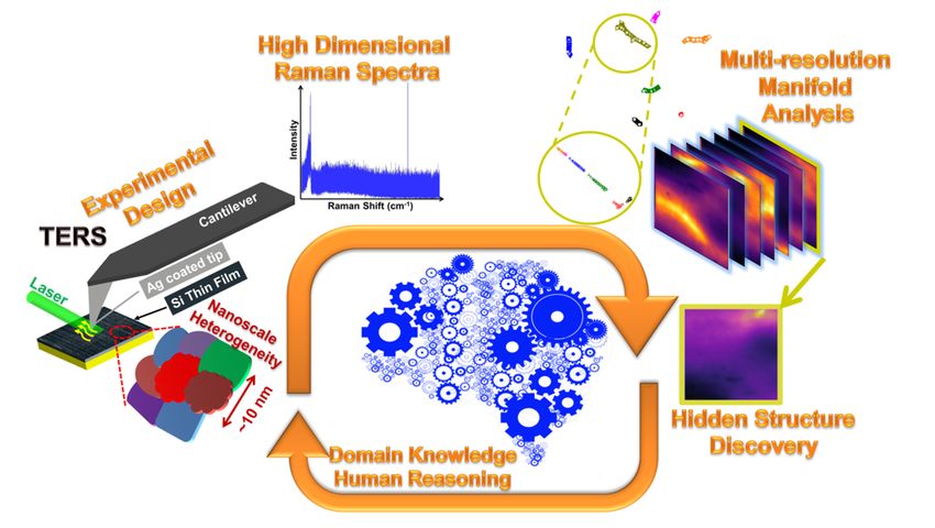
Abstract
Accurately identifying the local structural heterogeneity of complex, disordered amorphous materials
such as amorphous silicon (a-Si) is crucial for accelerating technology development. However, short-
range atomic ordering quanti cation and nanoscale spatial resolution over a large area on a-Si have
remained major challenges and practically unexplored. We resolve phonon vibrational modes of a-Si at a
lateral resolution of 20 nm by tip-enhanced Raman spectroscopy (TERS). To project the high dimensional
TERS imaging to a low dimensional (i.e. 2D) manifold space and categorize a-Si structure, we developed
a multiresolution manifold learning (MML) algorithm. It allows for quantifying average Si-Si distortion
angle and the strain free energy at nanoscale without a human-speci ed threshold. The MML
multiresolution feature allows for distilling local defects of ultra-low abundance (< 0.3%), presenting a
new Raman mode at ner resolution grids. This work promises a general paradigm of resolving
nanoscale structural heterogeneity and updating domain knowledge for highly disordered materials.

Introduction
Silicon is central for a gamut of applications including large-scale integrated electronic circuits, 1
photonics, 2 photovoltaics 3, 4 and energy storage units. 5, 6, 7 It is well known that the essences of Si-
based materials, including optical, electrical 8 properties and nuclear spin, 9 are highly related to their
atomic structures. Ever since Russell reported the rst observation of the rst-order inelastic Raman
scattering in a Si single crystal, 10 Raman spectroscopy has been intensively used to investigate the Si
crystal structure, 11 phonon dispersion, 12 electronic states, 13 local stress and strain, 14, 15 and thermal
properties, 16 which are integral to the performances of silicon-based devices. Despite its versatility, the
applications of micro-Raman spectroscopy to characterize the submicron-to-nanoscale chemistry and
physics are severely restrained by the intrinsic diffraction limit of the visible light (i.e. > 200 nm) based on
Abbe’s law. 17 Tip-enhanced Raman spectroscopy (TERS) provides an apertureless means of mapping
Raman scattering at nanometer scale (~ 10 nm) in-sample plane. 18, 19 This is based on that the surface
plasmon (i.e. enhanced electromagnetic eld or EM- eld) resides at the metallized tip apex of a scanning
probe microscope (SPM), providing a localized ”hot-spot” underneath the SPM tip. Consequently, the
Raman scattering of the sample within the hot-spot is largely increased, unraveling surface vibrational
modes with a nanoscale lateral resolution. 20 Sun et al. rst reported the successful TERS study on a Si
wafer. 21 With a 50% increase in the TERS intensity with respect to Raman, they were able to construct the
TERS mapping of the Si transverse optical (TO) mode (520 cm− 1) at ~ 100 nm resolution. Later, upon
optimization of the polarization conditions, Sokolov et al. improved the ratio of the near- eld Raman
intensity and far- eld Raman intensity by more than one order of magnitude, 22 hence being able to carry
out the nano-Raman analysis of the crystal Si at a ~ 20 nm lateral resolution.

Despite great efforts in deciphering the nanoscale vibrational structures on the Si surface using TERS, the
research focus has only been on crystal Si (c-Si) so far. Due to the highly symmetric diamond cubic
crystal structure of c-Si, its inelastic Raman shift carries the information re ecting optic phonon energy
                                                    Page 2/23
only at the center (i.e. Γ-point) of the rst-order Brillouin zone (BZ). 11, 23 Therefore, the spectral variation
on two adjacent sampling points is rather vague on TERS mapping.
Different from its c-Si counterpart, the energy states of amorphous silicon (a-Si) vary in the rst order BZ,
hence resulting in several convoluted Raman active modes. Due to k-selection rule breaking down for
amorphous materials, the TERS spectrum taken at each sampling point roughly corresponds to the
phonon density of states (PDOS), thereby capable of carrying local information of the a-Si. 11 However,
lacking the long-range atomic ordering and symmetries, to quantify the structure of amorphous materials,
such as a-Si remains a long-stand challenge. This is especially true for a large TERS dataset gathered
from a-Si over a large scanning area, which contains spectra collected from adjacent sampling points of
nanometers away sampling points. Accordingly, it is almost impossible to implement a manual
exploration over the structural metrics of the a-Si, let alone mining essential information of a miniature
structure embedded in such a large dataset. In addition, complex interactions between the tip-induced
EM- eld and Raman scattering tends to restrict the use of traditional linear dimension reduction
techniques, such as principal component analysis (PCA) (e.g. it becomes di cult to extract physical
information from unmixed components). 18 This explains why the nanoscale structural heterogeneity of
a-Si or other amorphous materials has been much underexplored by TERS so far.
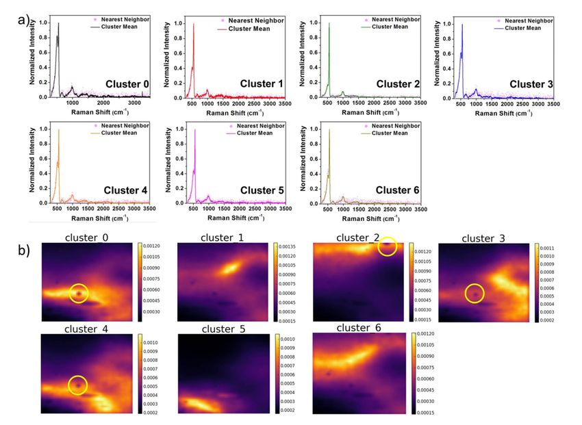
We herein illustrate a multiresolution analytical framework based on graph-analytics and an
unsupervised manifold learning algorithm to facilitate identifying the nanoscale structure of a-Si thin
lm. High-dimensional hyperspectral TERS mapping on the a-Si thin lm comprises thousands of TERS
spectra. The multiresolution manifold learning (MML) algorithm projects the TERS mapping to a low
dimensional (i.e. 2D) manifold space, thereby allowing for ease of straightforward data visualizations
and structural categorization. Unlike traditional manifold learning methods targeting solely on overlaying
the prior-known labels over the manifold points, 24the MML proposed here does not require any prior bias
regarding the material structure and instrumental modality. 25, 26 Bene ting from this nature, the
underlying a-Si structural and physical properties, such as the average Si-Si distortion angle and the
strain free energy can be quanti ed without a human-speci ed threshold at a lateral spatial resolution of
20 nm. Further, the multiresolution feature of the MML algorithm allows for extracting child clusters at the
ner resolution grid, which carries structural characteristics of minor abundance (< 0.3% of the sampling
points) that would have been hidden in the large dataset. It thus enables us to discover a new Raman
mode ascribed to highly disordered Ox-Si-Hy vibrations on a-Si surface that has never been reported
before. The identi cation of such a new vibrational Raman mode was further validated through inelastic
neutron scattering and density functional theory (DFT). Although a-Si was used as a model, the
integrated work ow proposed is readily available for nanoscale structure-property correlation for other
highly disordered materials in general.
Results And Discussion
Page 3/23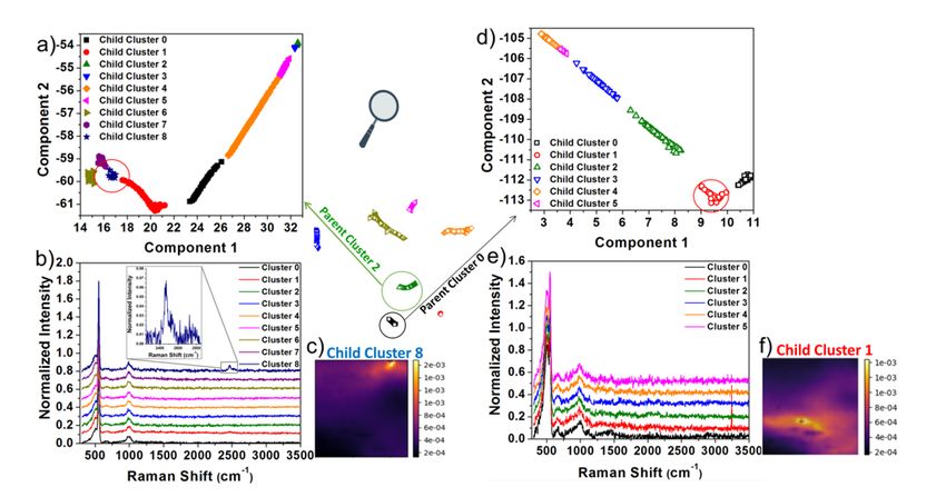
The strategy of effectively employing TERS hyperspectral imaging and the MML to elucidate the local
structure of the a-Si is schematically illustrated in Fig. 1. Brie y, TERS combines the scanning probe
microscopy (SPM) and the Raman spectroscopy technique, enabling the spectral acquisition at a
nanoscale lateral resolution. This is due to that the surface plasma resonance (SPR) on a noble metal
(such as Ag) coated tip apex upon laser illumination leads to a greatly enhanced EM- eld or a hot spot in
the gap between the tip and sample surface (< 5 nm in depth) (Figure S1(b)). 18 The Raman scattering
cross-section from the analyte in the hot spot is boosted, contributing to the far eld enhanced Raman
scattering (i.e. TERS spectrum). The area of a typical hot spot on the tip apex is on the scale of 10 nm,
thereby breaking the light diffraction limit of the standard confocal micro-Raman spectroscopy. 18, 22
However, the routine TERS mapping composes of innumerable spectra, precluding an easy insight of the
underlying structure. This is particularly true for amorphous materials. Therefore, it necessitates a more
statistical data processing method capable of implementing batch process of the large quantity TERS
spectra to e ciently obtain the structural features within the scanned area.

To explore relationships among all the high dimensional TERS spectra detailing the a-Si local structures,
we rst construct the nearest neighbor (NN) graph by calculating pairwise distances. For straightforward
exploration and visualization purpose, the low dimensional (2D/3D) manifold layout for the NN graph
was estimated by solving a principal probability model (details of graph construction and manifold
layout can be found at Method section). Clustering can be subsequently performed on the low-
dimensional manifold to underpin the intrinsic structure within the manifold that corresponds to the
material structure heterogeneity. To better partition intrinsic manifold clusters (facilitating clustering
tasks), Li et al. recently proposed a Graph-Bootstrapping procedure 25, 26 that iteratively reconstructed the
NN graph based on previous manifold positions and then recalculated manifold coordinates based on
the reconstructed NN graph. The projected low dimensional manifold clusters represent featured spectral
property of the materials, thereby allowing for gaining insights of latent material structures via external
validations such as rst principle theories. This, in turn, bene ts a future experimental design with
“human-reasoning” for gaining deeper structure-property relationship of the materials (Fig. 1).

The characteristic TERS spectra obtained from the a-Si surface is shown in Fig. 2(a). All spectra contain a
sharp peak located at 520 cm− 1, ascribed to the rst–order TO mode for the crystal silicon derived from
the TERS (Figure S3). For c-Si, only the zone-center TO mode is detectable based on the excitation of the
visible Raman laser to the lattices of the diamond structure, with the Si-Si bond angle of 109.5o. 10, 11, 27
Notably, the coexistence of the a-Si and c-Si TO modes in Fig. 2(a) does not indicate that the a-Si is
partially crystalized on the surface. 28 A further inspection on the a-Si surface using confocal micro-
Raman spectroscopy with a much higher laser power did not re ect the existence of the c-Si TO band at
520 cm− 1 (Figure S3). Instead, a few broad Raman bands were featured in several frequency regions,
indicating that the sputtered-silicon in this study is in totally amorphous state. The broadening of the
several Raman bands results from the loss of the long-range translational symmetry and corresponding
reciprocal lattice of the c-Si, which allows for detection of the entire phonon density of the states (DOS)
across the whole rst BZ zone re ected by the Raman spectra. 29 Though it is inappropriate to correlate
                                                   Page 4/23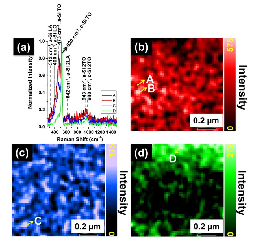
the traveling wave vectors to the phonon feature in amorphous solids, we assign the a-Si TERS bands to
phonon frequencies for ease of comparison with numerous other studies, 30, 31, 32, 33, 34 including the
modes of the longitudinal-acoustic (LA, 312 cm− 1), longitudinal-optical (LO, 400 cm− 1), transverse-optical
(TO, 473 cm− 1) and transvers-acoustic (TA, not shown here), respectively. 30 The second-order phonon
modes (denoted as 2LA and 2TO) of either a-Si or c-Si tip are also observable (Fig. 2(a)). The intensity of
the second order phonon modes is generally low, perhaps due to the off resonance of the laser frequency
with the a-Si direct band gap. 35 Due to the low signal-to-noise ratio, such second order phonon modes
are extremely di cult to be distinguished in standard Raman spectroscopy (Figure S3(b)) on a-Si,
corroborating the essential role of TERS in this study.

The TERS mapping is able to provide an overview of the intensity distribution of a given vibrational
mode. The normalized intensity (at 520 cm− 1 for TO mode) of each vibrational peak is quanti ed by the
color bar with the correspondence mapping representing the abundance of each chemical moiety.
Figure 2(b) presents the relative intensity distribution of the a-Si TO mode (approximately centered at
473 cm− 1). The TERS spectra taken from two spots (denoted as A and B) ~ 80 nm apart from each other
exhibit different TO mode intensity (Fig. 2(a)). This clearly indicates that the a-Si surface phonon mode
unveiled by TERS expresses nanoscale heterogeneity. TERS mapping of the a-Si 2LA mode is shown in
Fig. 2(c). Clearly, the feature of the intensity distribution of 2LA mode differs from that of the TO mode
shown in Fig. 2(b), demonstrating the highly heterogeneous feature of the phonon modes on a-Si surface.
It is also manifested the spectrum taken from Point C on the TERS map shows a larger 2LA mode
intensity than those from Points A and B, but the TO band intensity is lower than the latter two (Fig. 2(a)).
The a-Si 2TO mode at 943 cm− 1 has a favorable distribution on the upper side of the scanned region
(Fig. 2(d)), different from the distribution of the above-mentioned phonon modes. The TERS mapping
generated based on a single mode intensity clearly demonstrate that i) TERS is capable of depicting the
a-Si phonon mode in nanoscale, and ii) the abundance of different a-Si phonon modes is highly
heterogeneous and varies across the scanned area.

The mapping analysis based on the single variant method (i.e. intensity of a single TERS band)
insu cient to lead to a comprehensive understanding of the surface structure of the a-Si. 18 Analysis
based on an individual TERS band by its nature fails to capture the overall spectral pattern of TERS
mapping. To retain the global features embedded in the full set of TERS spectra, we then performed
manifold learning and clustering of TERS spectral dataset (see details in method section). Figure 3(a) is
the bootstrapped manifold layout of a set of 2500 TERS spectra, with evolution of manifold layouts
during Graph-Bootstrapping iteration procedure shown in Figure S4. The 2500 TERS spectra can be
categorized into seven clusters (Fig. 3(a)) in the 2D manifold space. Here we denote these clusters as
“parent clusters” to differentiate from the “child clusters” derived at ner resolution grids in manifold
space (see Fig. 5). The mean TERS spectrum of each cluster is shown in Fig. 3(b). An immediate
observation on Fig. 3(b) is that the TO band at ~ 470 cm− 1 intensity varies among clusters. The intensity
of the second order phonon peaks also varies, although not much obvious as the TO mode. To quantify
the analysis on the TERS bands below 600 cm− 1, we implemented peak deconvolution of the overlapped
                                                  Page 5/23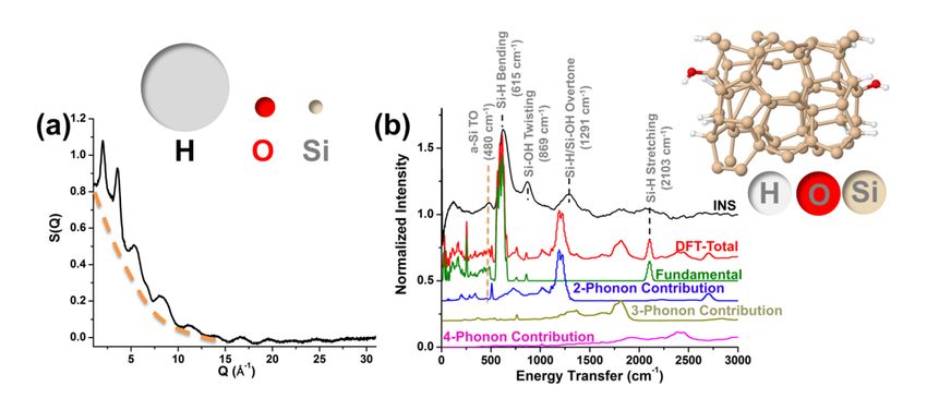
phonon vibrational modes of a-Si, including LA, LO, TO modes and c-Si TO mode. A TERS peak
deconvolution example is given in Fig. 3(c) based on the spectrum of cluster 0. The atomistic level local
structure of a-Si random network is characterized by the Si-Si bond angle and length distortion (Δθ), 33 Si-
ring topology (e.g. 5 or 6 membered rings), and voids. 36 The inelastic Raman scattering re ects the full
vibrational density-of-states (DOS). 37, 38 Therefore, the local structural change of the a-Si network can be
probed by the vibrational frequency change in Raman spectroscopy. Also given that the spring constant
for Si-Si bond stretching is much larger than that for bond bending, 39, 40 bond length distortions are
shown to contributes only 1% to the structural gap between a-Si and c-Si comparing with that of the bond
angle distortion. 41, 42 For TERS measurement, it is only sensitive to < 5 nm a-Si on surface (Figure S1).
Another major contribution towards the structural variation of a-Si also comes from the locally under- or
over- coordination of the a-Si network. 43, 44 However, as noted by an early study, the dangling or oating
Si bonds resulted from the under- or over- coordination counts from roughly 1% of the free energy
associated to the angle distortion. 41 In this context, we focus on the correlation between the average
bond angle distortions (Δθ) and the vibrational frequencies (ω) of the TERS spectra on a-Si. Here the
average bond angle distortion is de ned the Si-Si angle difference than 109.5°, representing the bond
angle in a tetrahedral repeating unit in c-Si.

Using a semiexperimental approach, Vink et al. 34 correlated the TO mode vibrational frequency (in cm− 1)
to the average bond angle distortions, Δθ (in angular degree), linearly as

Vink’s computational model was built based on a so-called activation-relaxation technique (ART), 45, 46
which yields close-to experimental a-Si atomic con gurations. Eq. 1 was found to agree reasonably well
with experimental values. Although it is generally accepted that the linear correlation between the feature
(i.e. the peak center and width) of the TO Raman peak with Δθ, 33, 34, 38, 47, 48 there still lacks a designative
quantitative agreement among all correlations between the two. Here we do not intend to seek a more
accurate correlation between the center of the TO mode and the Δθ, but rather to show that the TO modes
measured by TERS can be correlated to the a-Si local structure represented by Δθ. We rst rearranged the
Raman shift center of the TO mode taken from different clusters in a declining order as shown in
Fig. 3(d). Using Eq. 1, we can extract the local distortion angle (marked on Fig. 3(d)), ranging between 13
o   and 15 o. As noted by Beeman et al., 48 the absolute minimum distortion angle, Δθ was 6.6o for a
continuous a-Si network. Here, the local a-Si angular distortion angles taken from different regions are
greater than 13o, 12% of the 109.5°. The maximum distortion angle value was found to be 15° for Cluster
6 (Fig. 3(d)). This corresponds to the a-Si TO mode centered at 468 cm− 1, close to the lower limit of the
DOS of the optical branch for a-Si. 32 Therefore, the model a-Si thin lm used here features a highly
disordered random a-Si network on the surface. 33 The calculated strain energy based on the distortion

                                                    Page 6/23
angle is close to the upper limit of that reported by Tsu et al. 33, representing a highly strained a-Si surface
(Supporting Information).
So far, we have shown that the surface structure of a-Si explored by TERS can be identi ed by the MML
algorithm without a human-de ned threshold, which is meaningful to quantify the “poorly-de ned” a-Si
random network. To solidify this nding, we compare the experimental TERS spectra with the mean TERS
spectrum derived from each parent cluster in Fig. 4(a). For each cluster, the mean TERS spectrum closely
matches with its nearest neighbor, with mean absolute error percentage < 5%. In addition, the pairwise
Euclidean distance between the mean TERS spectrum and every as-measured TERS spectrum at each
pixel is used to check the variance in each cluster more quantitatively. More speci cally, the spatial
distribution of variance in the material space can be visualized by the similarity loadings (inversion of
pairwise Euclidean distances) in Fig. 4(b). For the similarity loading of each cluster, a pixel with higher
intensity represents a higher similarity between the corresponding experimental TERS spectrum and the
mean cluster TERS spectrum.
We note that the black singular patches in the similarity loadings (marked by yellow circles in Fig. 4(b))
indicate the local TERS spectra different from their surrounding area. To identify these singularities, we
performed sub-clustering within each parent cluster by MML. As shown in Fig. 5(a), Parent Cluster 2 was
divided into 9 child clusters at a ner resolution grid. An immediate observation is that Child Cluster 8 has
a distinguished TERS peak centered at 2435 cm− 1 (Fig. 5(b)). A closer exploration on the abundance
distribution of the TERS spectra (Fig. 5(c)) indicates that only 7 out of 2500 spectra represented by Child
Cluster 9 have the feature of the 2435 cm− 1 band. This manifests that the characterization strategy
developed in this study is sensitive to < 0.3% abundance of a structural minority embedded in a large data
set. A further inspection on all other singular points shown in the similarity loading maps in Fig. 4 does
not re ect TERS spectra carrying any physical meaning. For example, Patent Cluster 0 was
subcategorized into 6 child clusters at the ner resolution grid (Fig. 5(d-f)), with the Child Cluster 1
exhibiting a sharp spike at 3245 cm− 1. This spike stems from the cosmic ray commonly seen in Raman
spectroscopy. Therefore, it necessitates a careful inspection on all stemmed spectra analyzed by the
multiresolution method, emphasizing that the domain knowledge human resonating is an essential link in
Fig. 1.
The assignment of the 2435 cm− 1 TERS band is not intuitive (denoted as X-mode for now), since no
fundamental Si-Si vibrational modes exist in the vicinity of this frequency. It is thus reasonable to assume
other surface functional groups present on a-Si surface. Noting that the a-Si thin lm was RF sputtered in
an inert (i.e. argon) atmosphere in the current study, the as-sputtered a-Si surface should be enriched in
the unbounded Si atoms. Once exposed to air, we expect the components of the air instantaneously react
with dangling Si bonds. Further neutron scattering experiment indicates the presence of the protonated
spices on a-Si. As shown in Fig. 6(a), the rst con rmation of the proton presence in a-Si sample is the
plot of the structure factor, S(Q) (Q: scattering vector), with the contributions from both the coherent
scattering and incoherent scattering of the sample itself. 49 The anisotropic incoherent scattering cross
Page 7/23section of the proton is 80.26, > 37 times of the Si coherent scattering cross section at 2.163 (inset in
Fig. 6(a)). 50 Therefore, S(Q) plot exhibits a broad background shown in Fig. 6(a) due to incoherent
scattering from H. The reactions between the air water and dangling Si bond results in silane- and
siloxane- type moieties on a-Si (see Supporting Information).
The simplest protonated Si compound is Si-H. The reported Raman scattering center for monohydrate (Si-
H) ranges between 2030 cm− 1 51 and 2090 cm− 1. 52 Binding more protons to Si leads to blueshift of the
Si-H stretching mode, with the maximum frequency found for hydrogenated sputtered Si-H4 compound at
2189 cm− 1. 52 Given that the surface selection rule complied by TERS differs from those for IR and
Raman, 18 it is di cult to precisely predict the active TERS vibrational modes for SiHx compounds in this
frequency region.
Inelastic neutron scattering spectroscopy (INS) allows for measuring the vibrational modes in the
absence of the selection rules for hydrogen atom, 53 thereby exhibiting a comprehensive picture of all
possible vibrational modes on a-Si sample used here. Figure 6(b) shows an INS spectrum of the a-Si
sample. To unambiguously assign the vibrational modes, we further performed density functional theory
(DFT) calculation on a surface hydrogenated a-Si, assuming a “water splitting” mechanism (see
supporting information) to form the Si-H and Si-OH functional groups on a-Si surface (Fig. 6(b) inset).
The existence of the –H and –OH functional groups in the a-Si sample is validated by the excellent
agreement between the experimental INS spectrum and that calculated by DFT in Fig. 6(b). The most
distinguished proof of the Si-H bond presence is the Si-H bending mode centered at 615 cm− 1. The
presence of the Si-OH groups is evidenced by the Si-OH twisting bands centered at 869 cm− 1 from INS
spectrum. 54 Intriguingly, both experimental and DFT calculated INS spectra show a broad band at
around 2430 cm− 1, assigned to the 4-phonon overtone of the Si-H bending mode. In fact, the Si-H
stretching vibrational mode (frequency as ν) is closely related to the electronegativity of the near-neighbor
surroundings, with a simpli ed induction model formulated as 55
where νo and b are empirically derived constants and XA is de ned as the stability-ratio (SRX)
electronegativity. 56 The values of νo and b were found to be 1741 and 34.7 for molecular compounds,
respectively. 55 The sum is over three neighbors, assuming tetracoodination among the neighboring
atoms with the central Si. Different atomic species have various values of SRX, namely XSi = 2.62, XH =
3.55, and XO = 5.21. 54
In this context, the Si-H stretching mode can further blueshift to above 2250 cm− 1. 54, 57 Based on Eq. 2,
the highest possible frequency for Si-H stretching mode calculated is 2283 cm− 1 for O3-Si-H type
compound. However, this value is still 152 cm− 1 lower than the X-mode shown in TERS spectrum in
Page 8/23Parent Cluster 2, Child Cluster 8 (Fig. 5(b)). Given that the a-Si thin lm is highly disordered on the surface
intrinsically, we reason that there possibly exists overly coordinated surface Si atoms of low abundance.
We herein de ne Xe as the excess SRX electronegativity contributed from the excess coordination (> 4) to
the Si. For the case of X-mode of the TERS band, Xe was calculated at 4.4, close to the reported value for
the suboxide silicon as an effective media for a-Si. 54 In this case, the central Si may form the
orthosilicate-type compound with the oxygen in surrounding suboxide silicon. Thus, the large blueshift of
the X-mode TERS band than generally reported values stems from overcoordination of the Si-H with the
surrounding suboxide (Ox-Si-Hy, x + y > 4). Since in the same frequency region, as a bulk sensitive
spectroscopy technology, INS shows only a broad shoulder (Fig. 6(b)), the abundance of the
overcoordination Si compound should thus be critically low. It is therefore worth emphasizing that the
existence of the trace amount (< 0.3%) of the surface defects can only be validated by the ultra-surface
sensitive technology, TERS, with the structural information distilled by the MML algorithm.
Conclusions
We successfully demonstrate that the nanoscale structural heterogeneity of amorphous Si can be
identi ed and quanti ed by the synergy between TERS hyperspectral imaging and an unsupervised
machine learning-based manifold method. Straightforward clustering and visualization of the manifold
structure enable the detection of highly localized conformational changes of a-Si at atomistic level,
re ecting the underlying structural and physical essences of the a-Si, including the average Si-Si angle
distortions and the strain free energy, without prede ned threshold owing to its unsupervised nature. This,
in turn, facilitates to set a paradigm to categorize the highly disordered structure for amorphous
materials. The multiresolution capability of the MML algorithm allows for mining ultra-low abundance
structural information at a ner resolution grid. As a result, a new Raman mode of a-Si surface chemistry
embedded in a large TERS dataset can be detected. These insights are valuable for unraveling the
nanoscale structure, such as defects of semiconductor devices in both fundamental research and
industrial applications.
While current study solely focuses on a-Si thin lm, the combination of ultra-sensitive surface
spectroscopy, TERS and the e cient multiresolution manifold learning algorithm should boost scienti c
discoveries in a broad scope of disciplines, such as solid-state electrolytes, metal–organic framework
(MOF) and low-dimension materials, revealing the unknown unknowns to material and domain scientists.
Methods
TERS setup and measurements
A physical vapor deposition (PVD) method was used to fabricate TERS probes from commercial AFM tips
(Bruker, OTESPA-R3, resonance frequency = 300 kHz, spring constant = 26 N/m, tip apex diameter = 7
nm) as reported in a previous study. 18 Brie y, three sequential depositions of chromium (Cr) (2 nm
adhesion layer), silver (Ag, plasmonic layer, ~40 nm), and aluminum (Al, protection layer, 2 nm) were
Page 9/23performed. Al converts to a dense alumina that provides good mechanical and chemical protection
without in uencing signi cantly on tip optical properties. TERS tip fabrication details can be found in
Reference 58.
All TERS measurements were performed on an atomic force microscope (AFM, AIST-NT SMART PROBE)
in connection with a Raman spectrometer (HORIBA Co., Xplore) in an argon- lled glove box. For Raman
measurements, the 532 nm laser wavelength was chosen with a local power density of 25 µW. The
grating number was 600 grooves/mm, and the objective was 100× (N.A. = 0.7). The tapping mode was
chosen with oscillation amplitude of 20 nm and a ~ 2 nm minimum distance from the sample surface for
AFM. The mapped area was set at 1 × 1 µm2 with a step size 20 nm. The accumulation time was 0.5 s for
each spectral acquisition. Each frame of TERS map represents the intensity (after background correction)
of the corresponding vibrational mode that arises from a-Si.
FDTD simulation
Three-dimensional (3D) nite-difference time-domain (FDTD) simulations were used to study the
electromagnetic (EM- eld) distribution between the tip apex and the a-Si sample. The method was
detailed in our previous report, 18 and elaborated in supporting information (Figure S1).
Manifold Clustering
Low-dimensional manifold embedding for TERS measurements is calculated via a modi ed Graph-
Bootstrapping approach. 25, 26 Graph-Bootstrapping is an iterative procedure that consists of two main
steps: construction of nearest neighbor graph and manifold layout of nearest neighbor graph. During the
initialization (iteration 0) of Graph-Bootstrapping, a nearest neighbor graph is calculated based on the
high-dimensional TERS measurements, which we call this graph as root graph. Accordingly, we refer the
manifold layout of the root graph as root manifold. During the iteration of Graph-Bootstrapping, nearest
neighbor graph is reconstructed based on the low-dimensional manifold coordinates of the previous
iteration and subsequently manifold layout is updated based on the newly reconstructed graph.
Graph construction and manifold layout follows the way of LargeVis. 59 Approximate nearest neighbor
graph construction is calculated via random projection tree 60 and neighbor exploring 61 techniques, given
the input dataset X = {X1, X2, ……, Xn}⊆Rd. (Recall that, during the initialization of Graph-Bootstrapping
procedure, the input dataset X is the original TERS measurements of high dimensionality. During the
iterations of Graph-Bootstrapping, the input dataset X is the low-dimensional (d = 2) manifold
coordinates of the graph of previous iteration). Speci cally, the graph is rstly constructed by searching k
nearest neighbors via random projection tree method. The graph is then re ned via neighbor exploring
procedure: 1) Create the max-heap Hi for each node i in the graph; 2) For each neighbor node j of node i,
calculate Euclidean distances between node i and each neighbor node l of node j, dist(i,l) = ; 3) Push l
with dist(i,l) into Hi; 4) Pop if Hi has more than k nodes. For each node i and each neighbor node j of i, an
Page 10/23edge E(i,j) is added to the graph. The weight of symmetric edge E(i,j) is de ned in a similar way of t-sne
method : 62
To calculate a low-dimensional manifold layout of the graph where each node i of graph is represented
by a point yi in 2D space, a likelihood function is constructed to preserve pair-wise similarities of the
nodes in the 2D space, 59
Clustering on manifold is performed by hierarchical density estimates method (HDBSCAN), 67 that relies
on the mutual reachability distance:
D mreach,K(a,b) = max{corek(a), corek(b), d(a,b)}, Equation (5)
where d(a,b) is the original metric distance (Euclidean distance in this paper) between points a and b,
corek(x) is the core-distance of a point x to cover its k nearest neighbors. A minimum spanning tree is
rstly built and then condensed upon the hyper-parameter of minimum cluster size, mc. The stability of
each cluster Ci is de ned as:
where λ is the reciprocal of core-distance, λmax,Ci,a is the λ value at which point a falls out of cluster Ci and
λmin,Ci,a is the minimum λ value at which point a is present in Ci. Optimal at clusters are extracted via
walking up the tree to maximize the total stability score over chosen clusters: considering all leaf nodes
as initial clusters, if the cluster’ stability is greater than the sum of its child, the cluster is selected to be in
current set of optimal at clustering and all its child are removed from the set. Otherwise, the cluster’s
stability is set to be the sum of its child stabilities. The main tuning parameter is the minimum cluster
Page 11/23size, mc. We leave all the other tuning parameters of HDBSCAN as default. For the parent manifold
clusters in Figure 3, we follow a similar procedure in ref. 21 to choose mc. We rst consider all
integer mc values in a wide range of [10,150]. We then t the trend of total number of estimated clusters
against every mc value by the exponential decay function. We choose the mc in the tail region where the
total number of clusters tends to be stable. For child manifold clusters at the ner resolution grid as
shown in Figure 5, we set the mc a small value around 0.5% of the total number of TERS measurements.
Neutron Scattering
All neutron scattering measurements were performed at the Spallation Neutron Source at Oak Ridge
National Laboratory (ORNL). Prior to each measurement, the a-Si lm was peeled off from the copper
substrate in the Ar- lled glovebox (O2 < 0.1 ppm, H2O < 0.1 ppm) and sealed in a vanadium can (Ø = 6
mm). The total amount of a-Si was 1.368 g and the height was 3.9 cm. An empty vanadium can of the
same type was sealed in Ar-glovebox and used as a blank reference.
1. Neutron total scattering structure function. The structure function data was collected at Nanoscale-
Ordered Materials Diffractometer (NOMAD) beamline per a procedure published by Neuefeind et al.
68 The data collection time was 150 min. The structure factor, S(Q) was obtained from a Q range
between 0.5 and 31 Å−1.
2. Inelastic neutron scattering (INS). INS spectra were obtained at the VISION beamline on the same a-
Si measured by neutron PDF to assure consistency. The sample was measured in vanadium sample
holder at 5 K for about 10 hours. The empty sample holder was also measured, and the background
spectrum was removed to obtain the spectrum from the sample.
Molecular Dynamics (MD) simulations
The models of a-Si were established by conducting molecular dynamics simulations in LAMMPS.69
Following a melting-and-quench procedure, 70 the initial network a-Si was rstly annealed to 2400 K in the
NVT ensemble, and then quenched to room temperature (300 K) at a quench rate of 1012 Ks-1. The a-Si
models were nally fully relaxed at 300 K in the NPT ensemble. The SW-VBM interatomic potential 71 was
used to describe Si-Si interaction. The average coordination number of constructed a-Si models is ~3.99
and quite close to the experimental value (~ 3.8-3.9), 72, 73, 74 validating the high quality of these a-Si
models.
Density Functional Theory (DFT) calculations
Density Functional Theory (DFT) modeling was performed using the Vienna ab initio Simulation Package
(VASP).75 The calculation used Projector Augmented Wave (PAW) method 76, 77 to describe the effects of
core electrons, and Perdew-Burke-Ernzerhof (PBE) 78 implementation of the Generalized Gradient
Approximation (GGA) for the exchange-correlation functional. Energy cutoff was 600 eV for the plane-
wave basis of the valence electrons. The starting structure of a-Si slab with both surfaces terminated by
Page 12/23–H and -OH was generated by MD simulations as discussed above. 69 The thickness of the slab is about
1.5 nm, and the total thickness of the simulation box is 3.5 nm (i.e., 2 nm vacuum). The surface area is
about 1.05 nm × 1.05 nm. The simulation box contains 64 Si atoms, and is under 3D periodic boundary
condition. The electronic structure was calculated on a 3 × 3 × 1 Monkhorst-Pack mesh. The total energy
tolerance for electronic energy minimization was 10-5 eV, and the maximum interatomic force after
relaxation was below 0.01 eV/Å. The vibrational eigen-frequencies and modes were then calculated by
the nite displacement method. The OClimax software 79 was used to convert the DFT-calculated phonon
results to the simulated INS spectra.
Declarations
Acknowledgments
This work is supported by the U.S. Department of Energy's Vehicle Technologies O ce under the Silicon
Electrolyte Interface Stabilization (SEISta) Consortium directed by Brian Cunningham and managed by
Anthony Burrell. Part of this work was supported by The work was supported by the Center for
Nanophase Materials Sciences, a U.S. Department of Energy, O ce of Science User Facility at Oak Ridge
National Laboratory (S.V.K), Division of Materials Science and Engineering, Biomolecular Materials
Program, and Energy Frontier Research Center CSSAS located at University of Washington (X.L.). We
thank Dr. Dmitry N. Voylov for extremely useful discussion on the TERS experimental setup. We are
grateful for fruitful discussions on RF sputtering with Drs. Nancy J. Dudney, Andrew Kercher, and Robert
L. Sacci. We thank Drs. Andrew Westover, Jue Liu and Katharine L. Page discussion for NOMAD setup.
We thank Michelle S. Everett for strong technical support for NOMAD.
References
1. Chen R, et al. Nanophotonic integrated circuits from nanoresonators grown on silicon. Nature
communications 5, 1–10 (2014).
2. Vivien L, Pavesi L. Handbook of silicon photonics. Taylor & Francis (2016).
3. Ndiaye A, Charki A, Kobi A, Kébé CM, Ndiaye PA, Sambou V. Degradations of silicon photovoltaic
modules: A literature review. Solar Energy 96, 140–151 (2013).
4. Kim J, et al. 10.5% e cient polymer and amorphous silicon hybrid tandem photovoltaic cell. Nature
communications 6, 1–6 (2015).
5. Hou T, et al. The in uence of FEC on the solvation structure and reduction reaction of LiPF6/EC
electrolytes and its implication for solid electrolyte interphase formation. Nano Energy 64, 103881
(2019).
6. Wu H, et al. Stable cycling of double-walled silicon nanotube battery anodes through solid–
electrolyte interphase control. Nature nanotechnology 7, 310 (2012).
Page 13/237. Ryu J, et al. In nitesimal sulfur fusion yields quasi-metallic bulk silicon for stable and fast energy
storage. Nature communications 10, 1–9 (2019).
8. Hasan M, Huq MF, Mahmood ZH. A review on electronic and optical properties of silicon nanowire
and its different growth techniques. SpringerPlus 2, 151 (2013).
9. Kane BE. A silicon-based nuclear spin quantum computer. nature 393, 133 (1998).
10. Russell JP. Raman scattering in silicon. Applied Physics Letters 6, 223–224 (1965).
11. Parker Jr J, Feldman D, Ashkin M. Raman scattering by silicon and germanium. Physical Review 155,
712 (1967).
12. Richter H, Wang Z, Ley L. The one phonon Raman spectrum in microcrystalline silicon. Solid State
Communications 39, 625–629 (1981).
13. Yue G, Lorentzen J, Lin J, Han D, Wang Q. Photoluminescence and Raman studies in thin- lm
materials: Transition from amorphous to microcrystalline silicon. Applied Physics Letters 75, 492–
494 (1999).
14. De Wolf I. Micro-Raman spectroscopy to study local mechanical stress in silicon integrated circuits.
Semiconductor science and technology 11, 139 (1996).
15. Zeng Z, Liu N, Zeng Q, Lee SW, Mao WL, Cui Y. In situ measurement of lithiation-induced stress in
silicon nanoparticles using micro-Raman spectroscopy. Nano Energy 22, 105–110 (2016).
16. Perichon S, Lysenko V, Remaki B, Barbier D, Champagnon B. Measurement of porous silicon thermal
conductivity by micro-Raman scattering. Journal of Applied Physics 86, 4700–4702 (1999).
17. Wang X, Huang S-C, Hu S, Yan S, Ren B. Fundamental understanding and applications of plasmon-
enhanced Raman spectroscopy. Nature Reviews Physics, 1–19 (2020).
18. Nanda J, et al. Unraveling the Nanoscale Chemical Heterogeneity of Solid Electrolyte Interphase
using Tip-Enhanced Raman Spectroscopy (in press). Joule, (2019).
19. Yano T-a, et al. Tip-enhanced nano-Raman analytical imaging of locally induced strain distribution in
carbon nanotubes. Nature communications 4, 1–7 (2013).
20. Sonntag MD, Pozzi EA, Jiang N, Hersam MC, Van Duyne RP. Recent advances in tip-enhanced Raman
spectroscopy. J Phys Chem Lett 5, 3125–3130 (2014).
21. Sun W, Shen Z. A practical nanoscopic Raman imaging technique realized by near- eld
enhancement. Materials Physics and Mechanics 4, 17–21 (2001).
22. Lee N, et al. High contrast scanning nano-Raman spectroscopy of silicon. Journal of Raman
Spectroscopy: An International Journal for Original Work in all Aspects of Raman Spectroscopy,
Including Higher Order Processes, and also Brillouin and Rayleigh Scattering 38, 789–796 (2007).
23. Brockhouse B. Lattice vibrations in silicon and germanium. Physical Review Letters 2, 256 (1959).
24. Zhong M, et al. Accelerated discovery of CO2 electrocatalysts using active machine learning. Nature
581, 178–183 (2020).
25. Li X, Collins L, Miyazawa K, Fukuma T, Jesse S, Kalinin SV. High-veracity functional imaging in
scanning probe microscopy via Graph-Bootstrapping. Nature communications 9, 2428 (2018).
Page 14/2326. Li X, et al. Manifold learning of four-dimensional scanning transmission electron microscopy. npj
Computational Materials 5, 5 (2019).
27. Morell G, Katiyar R, Weisz S, Jia H, Shinar J, Balberg I. Raman study of the network disorder in
sputtered and glow discharge a-Si: H lms. Journal of applied physics 78, 5120–5125 (1995).
28. Tsu R, Gonzalez-Hernandez J, Pollak FH. Determination of the energy barrier for structural relaxation
in amorphous Si and Ge by Raman scattering. Solid state communications 54, 447–450 (1985).
29. Zallen R. The physics of amorphous solids. John Wiley & Sons (2008).
30. Morimoto A, Ooroza S, Kumeda M, Shimizu T. Raman studies on local structural disorder in silicon-
based amorphous semiconductor lms. Solid state communications 47, 773–777 (1983).
31. Voutsas A, Hatalis M, Boyce J, Chiang A. Raman spectroscopy of amorphous and microcrystalline
silicon lms deposited by low-pressure chemical vapor deposition. Journal of Applied Physics 78,
6999–7006 (1995).
32. Tsu R, Gonzalez-Hernandez J, Doehler J, Ovshinsky S. Order parameters in a-Si systems. Solid state
communications 46, 79–82 (1983).
33. Sinke W, Roorda S, Saris F. Variable strain energy in amorphous silicon. Journal of Materials
Research 3, 1201–1207 (1988).
34. Vink R, Barkema G, Van Der Weg W. Raman spectra and structure of amorphous Si. Physical Review
B 63, 115210 (2001).
35. Renucci J, Tyte R, Cardona M. Resonant Raman scattering in silicon. Physical Review B 11, 3885
(1975).
36. Treacy M, Borisenko K. The local structure of amorphous silicon. Science 335, 950–953 (2012).
37. Brodsky M, Cardona M. Local order as determined by electronic and vibrational spectroscopy:
amorphous semiconductors. Journal of Non-Crystalline Solids 31, 81–108 (1978).
38. Alben R, Weaire D, Smith Jr J, Brodsky M. Vibrational properties of amorphous Si and Ge. Physical
Review B 11, 2271 (1975).
39. Keating P. Effect of invariance requirements on the elastic strain energy of crystals with application
to the diamond structure. Physical Review 145, 637 (1966).
40. Tsu R. Structural characterization of amorphous silicon and germanium. In: Disordered
Semiconductors). Springer (1987).
41. Saito T, Karasawa T, Ohdomari I. Distortion energy distributions in the random network model of
amorphous silicon. Journal of Non-Crystalline Solids 50, 271–276 (1982).
42. Steinhardt P, Alben R, Weaire D. Relaxed continuous random network models:(I). Structural
characteristics. Journal of Non-Crystalline Solids 15, 199–214 (1974).
43. Vignoli S, Mélinon P, Masenelli B, i Cabarrocas PR, Flank A, Longeaud C. Over-coordination and order
in hydrogenated nanostructured silicon thin lms: their in uence on strain and electronic properties.
Journal of Physics: Condensed Matter 17, 1279 (2005).
Page 15/2344. Deringer VL, et al. Realistic atomistic structure of amorphous silicon from machine-learning-driven
molecular dynamics. The journal of physical chemistry letters 9, 2879–2885 (2018).
45. Barkema G, Mousseau N. Event-based relaxation of continuous disordered systems. Physical review
letters 77, 4358 (1996).
46. Mousseau N, Barkema G. Traveling through potential energy landscapes of disordered materials: The
activation-relaxation technique. Physical Review E 57, 2419 (1998).
47. Marinov M, Zotov N. Model investigation of the Raman spectra of amorphous silicon. Physical
review B 55, 2938 (1997).
48. Beeman D, Tsu R, Thorpe M. Structural information from the Raman spectrum of amorphous silicon.
Physical Review B 32, 874 (1985).
49. Squires GL. Introduction to the theory of thermal neutron scattering. Cambridge university press
(2012).
50. Sears VF. Neutron scattering lengths and cross sections. Neutron news 3, 26–37 (1992).
51. Volodin V, Koshelev D. Quantitative analysis of hydrogen in amorphous silicon using Raman
scattering spectroscopy. Journal of Raman spectroscopy 44, 1760–1764 (2013).
52. Brodsky M, Cardona M, Cuomo J. Infrared and Raman spectra of the silicon-hydrogen bonds in
amorphous silicon prepared by glow discharge and sputtering. Physical Review B 16, 3556 (1977).
53. Harrelson TF, et al. Identifying atomic scale structure in undoped/doped semicrystalline p3ht using
inelastic neutron scattering. Macromolecules 50, 2424–2435 (2017).
54. Tsu D, Lucovsky G, Davidson B. Effects of the nearest neighbors and the alloy matrix on SiH
stretching vibrations in the amorphous SiO r: H (0 < r < 2) alloy system. Physical Review B 40, 1795
(1989).
55. Lucovsky G. Chemical effects on the frequencies of Si-H vibrations in amorphous solids. Solid State
Communications 29, 571–576 (1979).
56. Sanderson RT. Chemical periodicity. Reinhold Pub. Corp. (1960).
57. Borghesi A, Guizzetti G, Sassella A, Bisi O, Pavesi L. Induction-model analysis of Siî ¸ H stretching
mode in porous silicon. Solid state communications 89, 615–618 (1994).
58. Barrios CA, Malkovskiy AV, Kisliuk AM, Sokolov AP, Foster MD. Highly stable, protected plasmonic
nanostructures for tip enhanced Raman spectroscopy. The Journal of Physical Chemistry C 113,
8158–8161 (2009).
59. Tang J, Liu J, Zhang M, Mei Q. Visualizing large-scale and high-dimensional data. In: Proceedings of
the 25th international conference on world wide web). International World Wide Web Conferences
Steering Committee (2016).
60. Dasgupta S, Freund Y. Random projection trees and low dimensional manifolds. In: STOC). Citeseer
(2008).
61. Dong W, Moses C, Li K. E cient k-nearest neighbor graph construction for generic similarity
measures. In: Proceedings of the 20th international conference on World wide web). ACM (2011).
Page 16/2362. Maaten Lvd, Hinton G. Visualizing data using t-SNE. Journal of machine learning research 9, 2579–
2605 (2008).
63. Mikolov T, Sutskever I, Chen K, Corrado GS, Dean J. Distributed representations of words and phrases
and their compositionality. In: Advances in neural information processing systems) (2013).
64. Li AQ, Ahmed A, Ravi S, Smola AJ. Reducing the sampling complexity of topic models. In:
Proceedings of the 20th ACM SIGKDD international conference on Knowledge discovery and data
mining). ACM (2014).
65. Tang J, Qu M, Wang M, Zhang M, Yan J, Mei Q. Line: Large-scale information network embedding. In:
Proceedings of the 24th international conference on world wide web). International World Wide Web
Conferences Steering Committee (2015).
66. Recht B, Re C, Wright S, Niu F. Hogwild: A lock-free approach to parallelizing stochastic gradient
descent. In: Advances in neural information processing systems) (2011).
67. Campello RJ, Moulavi D, Sander J. Density-based clustering based on hierarchical density estimates.
In: Paci c-Asia conference on knowledge discovery and data mining). Springer (2013).
68. Neuefeind J, Feygenson M, Carruth J, Hoffmann R, Chipley KK. The nanoscale ordered materials
diffractometer NOMAD at the spallation neutron source SNS. Nuclear Instruments and Methods in
Physics Research Section B: Beam Interactions with Materials and Atoms 287, 68–75 (2012).
69. Plimpton S. Fast parallel algorithms for short-range molecular dynamics. Journal of computational
physics 117, 1–19 (1995).
70. Sitinamaluwa H, Nerkar J, Wang M, Zhang S, Yan C. Deformation and failure mechanisms of
electrochemically lithiated silicon thin lms. RSC Advances 7, 13487–13497 (2017).
71. Vink R, Barkema G, Van der Weg W, Mousseau N. Fitting the Stillinger–Weber potential to amorphous
silicon. Journal of non-crystalline solids 282, 248–255 (2001).
72. Kugler S, et al. Neutron-diffraction study of the structure of evaporated pure amorphous silicon.
Physical Review B 40, 8030 (1989).
73. Fortner J, Lannin J. Radial distribution functions of amorphous silicon. Physical Review B 39, 5527
(1989).
74. Roorda S, et al. Structural relaxation and defect annihilation in pure amorphous silicon. Physical
review B 44, 3702 (1991).
75. Kresse G, Furthmüller J. E cient iterative schemes for ab initio total-energy calculations using a
plane-wave basis set. Physical review B 54, 11169 (1996).
76. Blöchl PE. Projector augmented-wave method. Physical review B 50, 17953 (1994).
77. Kresse G, Joubert D. From ultrasoft pseudopotentials to the projector augmented-wave method.
Physical Review B 59, 1758 (1999).
78. Perdew JP, Burke K, Ernzerhof M. Generalized gradient approximation made simple. Physical review
letters 77, 3865 (1996).
Page 17/2379. Cheng Y, Daemen L, Kolesnikov A, Ramirez-Cuesta A. Simulation of inelastic neutron scattering
spectra using OCLIMAX. Journal of chemical theory and computation 15, 1974–1982 (2019).
Figures
Figure 1
The integrated work ow comprising hyperspectral TERS imaging and the multi-resolution manifold
learning (MML) algorithm to depict a-Si structural heterogeneity at the nanoscale. The low dimensional
physical parameters characterizing material structures such as local defects and atomic vibrations are
translated into the high dimensional Raman spectra via hyperspectral TERS imaging transfer functions.
The intrinsic low dimensionality of the physics suggests the structure of TERS measurements on the
sample as a whole can be projected to a low dimensional latent manifold space via MML. Exploration
data analysis such as clustering can be e ciently conducted on the low-dimensional manifold space to
reveal salient features for evaluating material structure heterogeneity by human reasoning and updating
domain knowledge in a loop.
Page 18/23Figure 2
(a) TERS spectra collected from various locations on the a-Si surface labeled by “A” to “D” in (c-d). TERS
mapping of an individual peak intensity centered at (b) 473 cm-1 (a-Si TO mode), (c) 642 cm-1 (2LA
mode), and (d) 943 cm-1 (2TO mode). A hybrid TERS mapping combining the peak intensity distribution
in (b-d) is shown in Figure S2.
Page 19/23Figure 3
(a) The parent manifold layout via the Graph-Bootstrapping method (see details in Method section)
colored by the cluster labels. (b) The mean TERS spectrum for each cluster (spectrum normalized against
the c-Si TO band at 520 cm-1). (c) Peak deconvolution of the silicon TO modes, LO mode and LA mode.
(d) The TO-band center arranged in declining order. The error bar stands for the Gaussian tting deviation
of the peak center. Δθ is de ned as the deviation of the Si-Si bond angle in the a-Si random network from
that of the single crystal Si (109.5o).
Page 20/23Figure 4
(a) Average TERS spectrum of each cluster and its nearest neighbor in experimental data. (b) Similarity
loading of each cluster. The color bar represents the reciprocal of Euclidean distance between the mean
TERS spectrum and the as-taken TERS spectrum of each the pixel within a given cluster.
Page 21/23Figure 5
(a) An overview of child manifold clusters at the ner resolution grid, stemmed from Parent Cluster 2 and
(b) the corresponding mean TERS spectra of the child clusters. The peak centered at 2435 cm-1 of Child
Cluster 8 represents unique structural defects different from other child clusters. (c) Similarity loading of
Child Cluster 8 that shows a bright blob around the black singular patches in similarity loading of Parent
Cluster 2 in Figure 4. (d) Overview of child clusters stemmed from Parent Cluster 0 and (e) the
corresponding mean Raman spectra of the child clusters. (f) The similarity loading of Child Cluster 1 that
shows a bright blob around the black singular patches in Parent Cluster 0 similarity loading in Figure 4.
Page 22/23Figure 6
(a) Neutron scattering plot of the structure factor, S versus the scattering vector, Q collected from a-Si
under the same sputtering condition to deposit the a-Si thin lm. The dash curve guides the eye as an
indication of the background from incoherent scattering. Inset schematically illustrates the relative size of
the incoherent scattering cross section (XS) of proton (80.260), the coherent XS of oxygen (4.232) and
the coherent XS of silicon (2.163). (b) Comparison between the experimental inelastic neutron scattering
spectrum of the a-Si sample and that calculated using DFT based on the atomic conformations shown in
the inset image. The calculated total spectrum combines the fundamental vibrational modes and higher
order excitations up to 10 orders.
Supplementary Files
This is a list of supplementary les associated with this preprint. Click to download.
20200622SIcleanedGYJagjitNanda.docx
Page 23/23You can also read