ENHANCED PHOTOVOLTAIC PROPERTY BY FORMING P-I-N STRUCTURES CONTAINING SI QUANTUM DOTS/SIC MULTILAYERS
←
→
Page content transcription
If your browser does not render page correctly, please read the page content below
Cao et al. Nanoscale Research Letters 2014, 9:634
http://www.nanoscalereslett.com/content/9/1/634

 NANO EXPRESS                                                                                                                                     Open Access

Enhanced photovoltaic property by forming p-i-n
structures containing Si quantum dots/SiC
multilayers
Yunqing Cao, Peng Lu, Xiaowei Zhang, Jun Xu*, Ling Xu and Kunji Chen

  Abstract
  Si quantum dots (Si QDs)/SiC multilayers were fabricated by annealing hydrogenated amorphous Si/SiC multilayers
  prepared in a plasma-enhanced chemical vapor deposition system. The thickness of amorphous Si layer was
  designed to be 4 nm, and the thickness of amorphous SiC layer was kept at 2 nm. Transmission electron microscopy
  observation revealed the formation of Si QDs after 900°C annealing. The optical properties of the Si QDs/SiC multilayers
  were studied, and the optical band gap deduced from the optical absorption coefficient result is 1.48 eV. Moreover, the
  p-i-n structure with n-a-Si/i-(Si QDs/SiC multilayers)/p-Si was fabricated, and the carrier transportation mechanism was
  investigated. The p-i-n structure was used in a solar cell device. The cell had the open circuit voltage of 532 mV and the
  power conversion efficiency (PCE) of 6.28%.
  Keywords: Si quantum dots (Si QDs); Silicon carbide; Multilayers; Solar cell
  PACS: 81.07.Ta; 78.67.Pt; 88.40.jj

Background                                                                             Si-rich silica (SRO)/SiO2 multilayers and observed that
Recently, Si-based solar cells have been widely used due                               the shift of the spectral response range with changing
to its abundance, contaminant-free, and mature fabri-                                  the size of Si QDs from 3 to 8 nm [7]. However, the
cation process. However, for a single p-n junction crys-                               large band offset between Si and SiO2 causes the low
talline silicon solar cell, the maximum theoretical power                              carrier tunneling probability, which may deteriorate the
conversion efficiency is only 29.8%, because of the                                    performance of devices.
inevitable longer and shorter wavelength loss [1]. Since                                 Compared with SiO2, amorphous silicon carbide (a-SiC)
the low-dimensional Si quantum dots (Si QDs) have                                      has a lower band gap, which is helpful for enhancing the
quantum confinement effect, the band gap of Si QDs                                     carrier transport efficiency to improve the device perform-
can be tunable by controlling the dot size, which pro-                                 ance [8]. Recently, the structural and physical properties
vides an effective way to adjust the energy band struc-                                of Si QDs embedded in amorphous SiC matrix have been
tures by changing the Si QDs size to get better spectral                               studied [9,10]. Kurokawa et al. found that Si QDs can
matching [2,3]. It was reported that the broadband spec-                               be formed by thermal annealing amorphous SiC films,
tral absorption can be realized by forming the all Si-                                 and the photoluminescence band was redshifted with
based tandem type solar cells, whose power conversion                                  increasing Si QDs size [11]. Song et al. designed the
efficiency can exceed the Shockley-Queisser limit [4-6].                               p-typeek Si QDs: SiC/n-type c-Si heterojunction device
In the present stage, it is interesting to study the photo-                            and achieved the open circuit voltage, short circuit
voltaic properties of Si QDs-based structures for their                                current density, and fill factor of 463 mV, 19 mA/cm2,
actual applications in devices. For example, Park et al.                               and 53%, respectively [12].
studied Si QDs/c-Si heterojunction solar cells based on                                  In our previous works, Si QDs/SiO2, Si QDs/SiNx, and
                                                                                       Si QDs/SiC multilayers were fabricated by thermal anneal-
* Correspondence: junxu@nju.edu.cn                                                     ing of amorphous Si/SiO2, Si/SiNx, and Si/SiC multilayered
National Laboratory of Solid State Microstructures and School of Electronic            structures [13-15]. An intense electroluminescence (EL)
Science and Collaborative Innovation Center of Advanced Microstructures,
Nanjing University, Nanjing 210093, China
                                                                                       was achieved in Si QDs/SiC multilayers and the EL peak

                                        © 2014 Cao et al.; licensee Springer. This is an Open Access article distributed under the terms of the Creative Commons
                                        Attribution License (http://creativecommons.org/licenses/by/4.0), which permits unrestricted use, distribution, and reproduction
                                        in any medium, provided the original work is properly credited.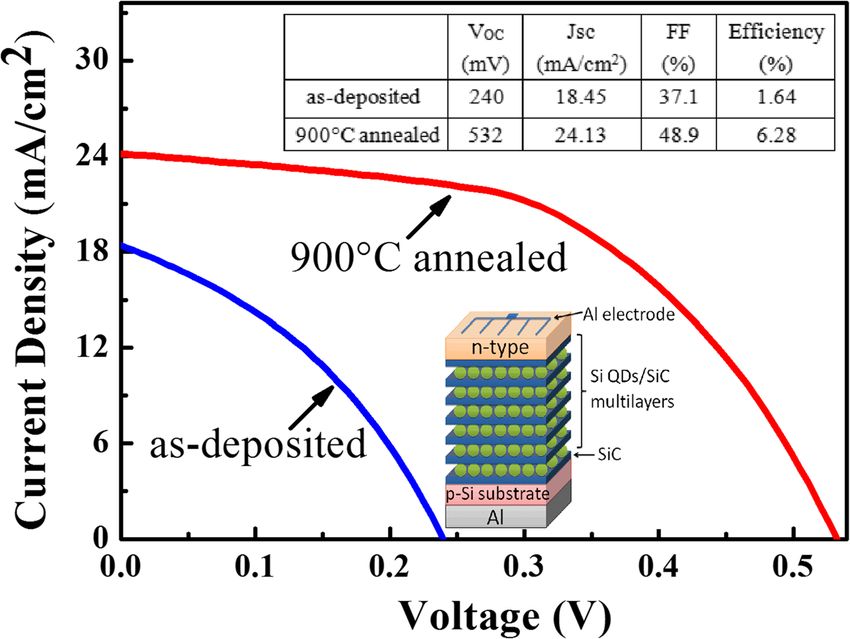
Cao et al. Nanoscale Research Letters 2014, 9:634                                                                        Page 2 of 6
http://www.nanoscalereslett.com/content/9/1/634

energy redshifted with increasing the Si QDs size, which in-   evaporated on both the surface and rear side of p-type
dicated the quantum confinement effect [16,17]. In the         Si wafer. The cell area was about 0.8 cm2. The illumi-
present work, hydrogenated amorphous Si (a-Si:H)/SiC           nated current-voltage (I-V) characteristics of the cell
multilayers were fabricated in a conventional plasma-          device were measured under an AM 1.5 (100 mW/cm2)
enhanced chemical vapor deposition (PECVD) system. The         illumination by using a Keithley 610C electrometer
thickness of a-Si:H was designed to be 4 nm, and the thick-    (Keithley 610C electrometer, Minato-ku, Japan).
ness of amorphous SiC layer was 2 nm. Due to the con-
strained crystallization principle, Si QDs with controllable   Results and discussion
size were achieved by annealing the as-deposited samples       Figure 1 shows the Raman spectra of as-deposited and
at 900°C for 1 h. The microstructures of samples before        900°C annealed multilayered samples. It is noted that
and after annealing were examined by cross-sectional trans-    only one broad band centered at 480 cm−1 exists in the
mission electron microscopy (x-TEM) and Raman spec-            as-deposited sample, which is attributed to the trans-
troscopy, which revealed the formation of Si QDs after         verse optical (TO) mode of amorphous Si-Si bonds.
thermal annealing. The optical properties were character-      However, an intense peak at 517 cm−1 associated with
ized by optical absorption measurements. Moreover, the p-      crystallized Si TO mode appears for 900°C annealed
i-n structure with n-a-Si/i-(Si QDs/SiC multilayers)/p-Si      sample, which indicates that the amorphous Si layers
was fabricated, which exhibits the photovoltaic properties     have been crystallized to form nano-crystallized Si. In
with the power conversion efficiency of 6.28%.                 order to estimate the crystallinity ratio and size of Si
                                                               QDs, we fitted the Raman spectrum via the Gaussian de-
Methods                                                        convolution by three components, which is located at
The a-Si:H/SiC multilayers (MLs) with six periods were         480, 510, and 520 cm−1. The crystallinity ratio (Xc) is
fabricated on quartz and p-Si substrates in a PECVD            figured out as 49.5% by integrated Gaussian peaks of 520
system. The a-Si sublayer was deposited by using pure          and 480 cm−1 [19]. The average size of Si crystals is
silane (SiH4), while the a-SiC layer was deposited by          about 4.8 nm, according to the phonon confinement
using a gas mixture of SiH4 and methane (CH4) with the         model [20], which indicates the formation of nano-
gas ratio R (R = [CH4]/[SiH4]) of 10. In our previous          crystalline Si quantum dots.
work, it was found that the collection efficiency of              The cross-sectional TEM measurements were per-
photo-generated carriers was improved by reducing the          formed to further characterize the multilayered struc-
thickness of SiC barriers [18]. In the present case, the       tures before and after annealing. Figure 2 is the cross-
thickness of a-Si:H layer was designed to be 4 nm, and         sectional TEM image of as-deposited a-Si (4 nm)/a-SiC
the thickness of amorphous SiC layer was kept at 2 nm.         (2 nm) MLs. The layered structures and smooth inter-
During the deposition process, the radio frequency             faces of Si/SiC can be clearly identified. The thickness of
power and the substrate temperature was kept at 30 W           a-SiC sublayer is 1.9 nm and the thickness of a-Si sub-
and 250°C, respectively. The post-treatment performed          layer is 4.2 nm, respectively, which is very close to the
in N2 atmosphere included two steps: dehydrogenation           pre-designed value estimated from the deposition rate.
at 450°C for 1 h and subsequently annealing at 900°C for       Figure 3a shows the cross-sectional TEM image of Si
1 h. The structural change of the Si/SiC MLs before and
after annealing was evaluated by Raman spectroscopy
(Jobin Yvon Horiba HR800 spectrometer, Kyoto, Japan).
The formation of Si QDs was determined by transmis-
sion electron microscopy (TEM) using Technai G2 oper-
ated at 200 KV. The optical absorption of the Si/SiC
MLs was measured at room temperature by Shimadzu
UV-3600 spectrophotometer (Shimadzu UV-3600 spec-
trophotometer, Kyoto, Japan).
   All Si-based solar cell containing Si QDs (4 nm)/SiC
(2 nm) MLs and 10 nm-thick phosphorus-doped amor-
phous Si layer were fabricated on p-type Si wafer (with a
thickness of 450 μm and a resistivity in the range of 1 to
bk3 Ω•cm) to get p-i-n solar cell structure. The n-layer
was deposited by a gas mixture of phosphorane (PH3) (1%
in H2) and SiH4 with the ratio of [PH3]/[SiH4] = 10. As a
                                                                Figure 1 Raman spectra of samples. As-deposited Si/SiC multilayers
reference, a-Si/SiC multilayer-based p-i-n structure was
                                                                (black line) and 900°C annealed Si/SiC multilayers (red line).
also fabricated at the same time. Al electrode was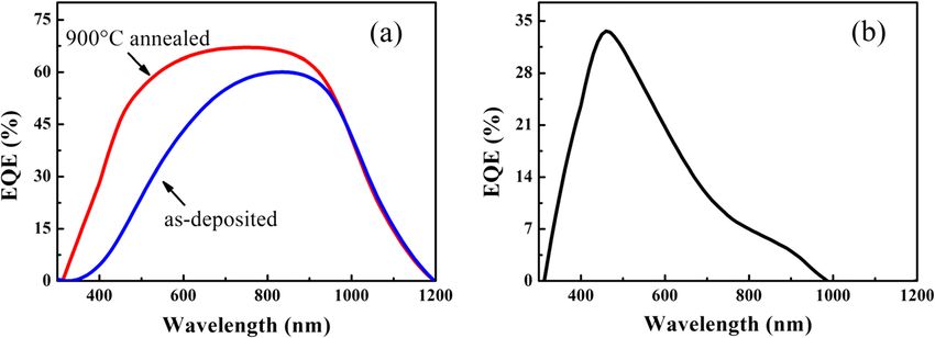
Cao et al. Nanoscale Research Letters 2014, 9:634 Page 3 of 6
http://www.nanoscalereslett.com/content/9/1/634
The optical absorption coefficient α is calculated and
given in Figure 4. It is found that the optical absorption
of as-deposited a-Si/SiC MLs is quite high, which is
above 105 cm−1 when the wavelength is less than 400 nm.
However, the absorption coefficient of 900°C annealed Si
QDs/SiC MLs is much higher in the whole visible light re-
gion (300 to 800 nm), which indicates that the Si QDs/SiC
MLs can strongly absorb the visible light photons, espe-
cially in short-wavelength range. Based on the Tauc model,
the optical band gap of Si QDs/SiC MLs can be deduced
from the linear fitting of (αhν)1/2 ~ hν relationship [21], as
shown in the inset of Figure 4. The deduced optical band
gap of our MLs after 900°C annealing is 1.48 eV, which is
blueshifted compared to that of crystallized Si, which can
be attributed to the quantum size effect [22]. In our previ-
ous work, we found that the optical band gap of Si QDs/
SiC MLs is enlarged with reducing the dot size, which
resulted in the blueshift of electroluminescence peaks.
We used a modified effective mass approximation (EMA)
Figure 2 Cross-sectional TEM image of as-deposited a-Si model to estimate the band gap of Si QDs/SiC MLs
(4 nm)/a-SiC (2 nm) multilayers. instead of infinite barrier model by considering the
Coulomb effect and the correlation energy terms [23].
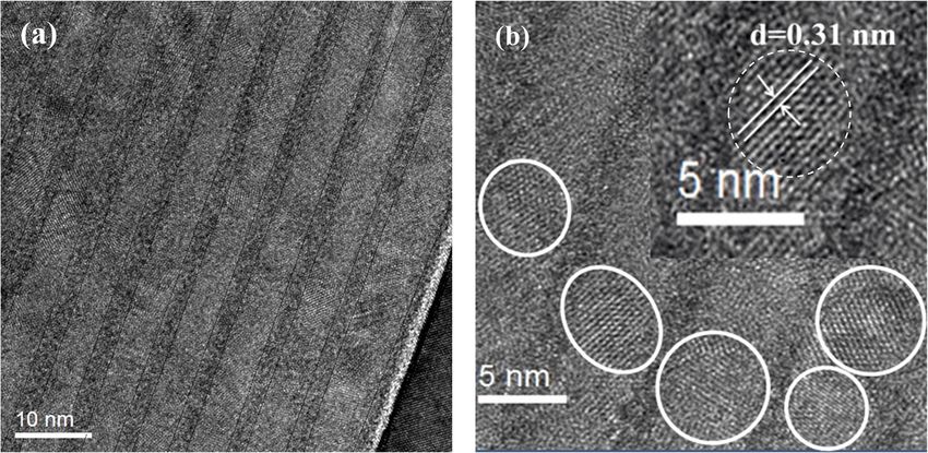
QDs/SiC MLs after 900°C annealing. The periodically Based on this model, the optical band gap (Egopt) can be
layered structures are well kept and the interfaces are expressed as follows:
still smooth and abrupt. The total thickness of the Si
QDs/SiC MLs is about 40 nm. The formation of Si QDs 0:4512
E g opt ¼ 1:12ðeVÞ þ ΔEe;h;reduced − −0:003394ðeVÞ
in a-Si layers can be identified in the high-resolution R
TEM image. As given in Figure 3b, the average size is
about 5 nm, which is well agreement with the Raman re- where 1.12 is the band gap of crystalline silicon, R is
sult. As indicated in the inset of Figure 3b, the crystal- the average diameter of Si QDs, 0.4512 is the Coulomb
line interplanar spacing is 0.31 nm of formed Si QDs, coefficient, 0.003394 is the correlation energy terms, and
which suggests the Si (111) crystalline faces. ΔEe,h,reduced is the decreased confinement energy related
The optical properties of Si/SiC MLs deposited on with the barrier height in conduction and valence band.
quartz substrate before and after annealing are studied According to the formula, the estimated band gap of Si
by measuring the optical transmission spectra and re- QDs with dot size of 4 to 5 nm is 1.4 to 1.5 eV, which is
flection spectra in the spectral range of 200 to 800 nm. in agreement with the experimental result.
Figure 3 Cross-sectional TEM image of 900°C annealed Si (4 nm)/SiC (2 nm) multilayers. (a) The cross-sectional TEM image of Si QDs/SiC
MLs after 900 °C annealing. (b) The high-resolution TEM image, in which the formed Si QDs can be clearly identified.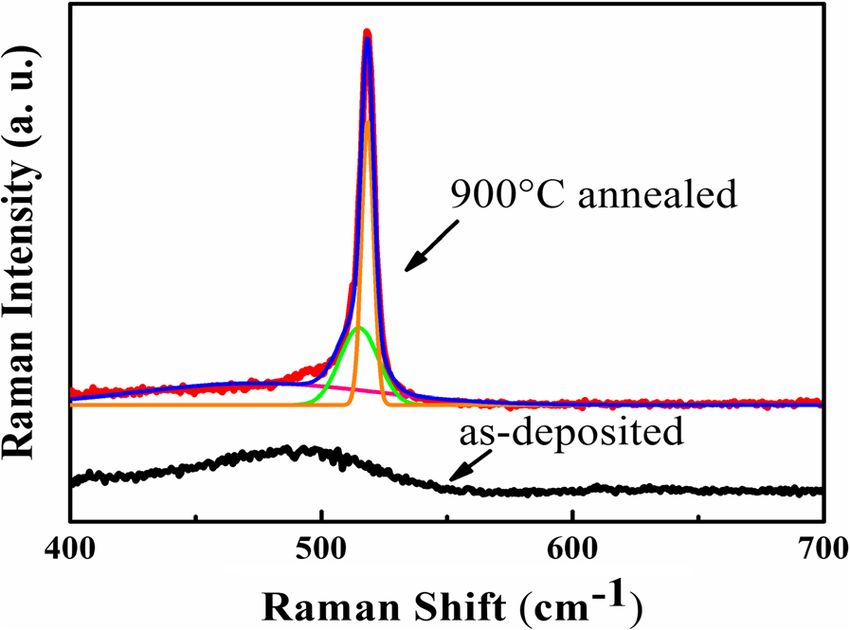
Cao et al. Nanoscale Research Letters 2014, 9:634                                                                        Page 4 of 6
http://www.nanoscalereslett.com/content/9/1/634

                                                                      sample can be attributed to the increase of the conductivity
                                                                      in crystallized Si layers. In our previous work, we found that
                                                                      the dark conductivity of prepared a-Si: H film is about
                                                                      4 × 10⁻⁹ S/cm and the conductivity reaches to 2 × 10⁻⁷ S/
                                                                      cm after 1,000°C thermal annealing [24]. It is reasonable
                                                                      to assume that the resistance in Si QDs/SiC MLs is also
                                                                      reduced after annealing due to the enhancement in the
                                                                      carrier transport properties, which results in the improve-
                                                                      ment of the rectification ratio of annealed p-i-n structure
                                                                      containing Si QDs/SiC MLs.
                                                                         The prototype solar cell devices were fabricated by
                                                                      evaporating the Al strip-shaped electrode on the p-i-n
                                                                      structures, and the cell area is about 0.8 cm2. Figure 6 is
                                                                      the AM 1.5 (100 mW/cm2) illuminated I-V curves of
 Figure 4 Optical absorption coefficient spectra of Si/SiC
 multilayers. As-deposited (blue line) and 900 °C annealed samples    solar cells based on as-deposited and 900°C annealed p-
 (black line). The inset is the (αhν)1/2 ~ hν relationship of 900°C   i-n structures, and inset of Figure 6 is the schematic dia-
 annealed sample.                                                     gram of the device structures. As shown in Figure 6, the
                                                                      open circuit voltage (Voc), short circuit current density
                                                                      (Jsc), and fill factor (FF) for the device based on as-
   Based on the structural and optical properties of pre-             deposited p-i-n structure is 240 mV, 18.45 mA/cm2, and
pared Si/SiC MLs, we fabricated the p-i-n device struc-               37.1%, respectively. The power conversion efficiency
tures containing phosphorus-doped a-Si: H and Si QDs/                 (PCE) is about 1.64%. However, the device performance
SiC (or a-Si/SiC) MLs on p-Si substrates. Figure 5 shows              of p-i-n structure containing Si QDs/SiC MLs after an-
the current-voltage (I-V) relationships of p-i-n structures           nealing is significantly enhanced. The Voc is increased to
with and without annealing. The rectification character-              532 mV, and the Jsc is increased to 24.13 mA/cm2 with
istics are clearly observed for both samples which indi-              the FF of 48.9%; the PCE reaches to 6.28%. The in-
cate that the p-i-n structures are well formed by the                 creased Voc of the annealed cell compared to that of as-
present approach. Compared with that of as-deposited                  deposited one can be attributed to the increased film
sample, the reverse current of annealed sample is in the              quality as well as the improved p-i-n structure after an-
same order (approximately 10−2 mA at −3 V) while the                  nealing. For as-deposited sample containing a-Si: H/SiC
forward current is increased by almost two orders of                  MLs, high density of defect states, such as dangling
magnitude (from 100 to 102 mA at +3 V), which indi-                   bonds and interface states between amorhous Si and SiC
cates that the rectification ratio of 900°C annealed p-i-n            layers, may lead to the pining of the Fermi levels which
structure reaches to 2 × 10³ at the applied voltage V = ±3 V.         results in the low Voc. After high-temperature annealing,
The increase in the forward current of annealed p-i-n                 the film quality can be significantly improved [25], which
                                                                      is helpful for increasing Voc by reducing the defect
                                                                      states. Moreover, post-annealing can also improve the p-
                                                                      i-n structure. As shown in Figure 5, the obvious rectifi-
                                                                      cation behavior can be observed in the annealed p-i-n
                                                                      structure. The shunt resistance of cell device is increased
                                                                      from 56 Ω to 108 Ω after annealing, which also indicates
                                                                      the improved p-i-n structure after annealing, due to the
                                                                      improved interface quality and the enhanced doping ef-
                                                                      fect in n-a-Si layer by thermally activating dopants. The
                                                                      present result is obviously improved compared with that
                                                                      of solar cell based on Si QDs/SiO2 MLs [26] and is com-
                                                                      patible with the reported values with other groups by
                                                                      using Si QDs/SiC. For example, Song et al. designed the
                                                                      p-type Si QDs: SiC/n-type c-Si heterojunction device
                                                                      and achieved the Voc, Jsc, and PCE of 463 mV, 19 mA/cm2,
                                                                      and 4.66%, respectively [12]. The improvement in the cell
 Figure 5 Current-voltage relationships of p-i-n structures.          performance for annealed sample can be attributed to the
 As-deposited (dashed line) and 900°C annealed samples (solid line)
                                                                      formation of Si QDs after 900°C annealing, which en-
 with p-i-n structures.
                                                                      hances the photon-generated carrier separation and
Cao et al. Nanoscale Research Letters 2014, 9:634 Page 5 of 6 http://www.nanoscalereslett.com/content/9/1/634 Figure 6 One-sun-illuminated current-voltage curves of solar cells. As-deposited (blue line) and 900°C annealed samples (red line) with p-i-n structures; inset is the schematic diagram of the device structure. carrier transportation properties due to the improved contribution of Si QDs, we give the EQE result of p-i-n electronic property of p-i-n structure. solar cell containing Si QDs/SiC MLs by subtracting the In order to further understand the role of Si QDs in the EQE of cell containing as-deposited one. As shown in present cell device, we measured the external quantum ef- Figure 7b, the improved EQE is located at the spectral ficiency (EQE) of p-i-n device sample and compared with range of 300 to 1,000 nm with the peak at 500 nm. As that of the as-deposited one. Figure 7a is the EQE of p-i-n mentioned before, the optical band gap of the Si QDs/SiC device structures containing as-deposited and 900°C MLs in our case is about 1.5 eV (approximately 820 nm), annealed Si/SiC MLs in the spectral range of 300 to 1,200 and the incident photons with high energy can be effect- nm. It is found that in the long wavelength region, the ively absorbed by Si QDs to generate the electron-hole EQE results for two cells are almost the same. However, pairs which are separated by the built-in field in p-i-n the EQE is significantly improved in the whole visible light structure. The electrons and holes can be effectively col- region (300 to 900 nm), which can be attributed to the lected in the annealed sample due to its improved carrier contribution of the formed Si QDs in annealed sample. transportation properties as shown in Figure 5. It is worth In our cell devices, part of the carriers was generated from noting that parameters of the present cells have not been Si substrates with the incident photons with long wave- optimized, and there is no any light trapping structures length. They contributed to the Jsc both in as-deposited used. The optimized design and processing control can and annealed cells. In order to further investigate the further improve the cell performance. Figure 7 External quantum efficiency of solar cells. (a) The EQE results of p-i-n device structures containing as-deposited (blue line) and 900° C annealed (red line) Si/SiC MLs. (b) The EQE results of p-i-n solar cell containing Si QDs/SiC MLs by subtracting the EQE of cell containing as-deposited one.
Cao et al. Nanoscale Research Letters 2014, 9:634                                                                                                        Page 6 of 6
http://www.nanoscalereslett.com/content/9/1/634

Conclusions                                                                        7.      Park S, Cho EC, Song DY, Conibeer G, Green MA: n-Type silicon quantum
In summary, we fabricated Si QDs/SiC MLs by anneal-                                        dots and p-type crystalline silicon heteroface solar cells. Sol Energy Mater
                                                                                           Sol Cells 2009, 93:684–690.
ing a-Si: H/SiC MLs at 900°C with amorphous Si thick-                              8.      Jiang CW, Green MA: Silicon quantum dot superlattices: modeling of
ness of 4 nm and amorphous SiC thickness of 2 nm.                                          energy bands, densities of states, and mobilities for silicon tandem solar
Cross-sectional TEM observation reveals that the Si                                        cell applications. J Appl Phys 2006, 99:114902.
                                                                                   9.      Cheng QJ, Tam E, Xu SY, Ostrikov K: Si quantum dots embedded in an
QDs were formed after annealing, and the average dot                                       amorphous SiC matrix: nanophase control by non-equilibrium plasma
size is around 4.8 nm. It is found that the optical absorp-                                hydrogenation. Nanoscale 2010, 2:594–600.
tion edge is blueshifted compared with the c-Si, and the                           10.     Chang GR, Ma F, Ma DY, Xu KW: Multi-band silicon quantum dots
                                                                                           embedded in an amorphous matrix of silicon carbide. Nanotechnology
optical band gap is about 1.48 eV, which is well agree-                                    2010, 21:465605.
ment with the theoretical estimation by using modified                             11.     Kurokawa Y, Tomita S, Miyajima S, Yamada A, Konagai M:
EMA model. Moreover, the p-i-n device structures con-                                      Photoluminescence from silicon quantum dots in Si quantum
                                                                                           dots/amorphous SiC superlattice. Jpn J Appl Phys 2007, 46:L833–L835.
taining Si/SiC MLs were fabricated. Improved rectifica-                            12.     Song DY, Cho EC, Conibeer G, Flynn C, Huang YD, Green MA: Structural,
tion characteristics were observed in annealed sample                                      electrical and photovoltaic characterization of Si nanocrystals embedded
compared with that in as-deposited one and the rectifi-                                    SiC matrix and Si nanocrystals/c-Si heterojunction. Sol Energy Mater Sol
                                                                                           Cells 2008, 92:474–481.
cation ratio is about 2,000. The enhanced photovoltaic                             13.     Wang MX, Chen KJ, He L, Li W, Xu J, Huang XF: Green electro- and
properties were observed in both annealed and as-                                          photoluminescence from nanocrystalline Si film prepared by continuous
deposited p-i-n cell devices. The cell containing Si QDs/                                  wave Ar+ laser annealing of heavily phosphorus doped hydrogenated
                                                                                           amorphous silicon film. Appl Phys Lett 1998, 73:105–107.
SiC MLs has the Voc of 532 mV, Jsc of 24.1 mA/cm2, and                             14.     Wu W, Huang XF, Chen KJ, Xu JB, Gao X, Xu J, Li W: Room temperature
PCE of 6.28%. The improvement in EQE result for                                            visible electroluminescence in silicon nanostructures. J Vac Sci Technol A
annealed cell device can be attributed to the formation                                    1999, 17:159–163.
                                                                                   15.     Rui YJ, Li SX, Xu J, Cao YQ, Li W, Chen KJ: Comparative study of
of Si QDs which enhances the absorption of incident                                        electroluminescence from annealed amorphous SiC single layer and
photons, especially in the short wavelength range and                                      amorphous Si/SiC multilayers. J Non-Cryst Solids 2012, 358:2114–2117.
the carrier transportation process. Our experiment results                         16.     Rui YJ, Li SX, Cao YQ, Xu J, Li W, Chen KJ: Structural and
                                                                                           electroluminescent properties of Si quantum dots/SiC multilayers. Appl
infer that the Si QDs/SiC MLs can be used as a potential                                   Surf Sci 2013, 269:37–40.
candidate for advanced optoelectronic devices.                                     17.     Chen DY, Wei DY, Xu J, Han PG, Wang X, Ma ZY, Chen KJ, Shi WH, Wang
                                                                                           QM: Enhancement of electroluminescence in p–i–n structures with
Abbreviations                                                                              nano-crystalline Si/SiO2 multilayers. Semicond Sci Technol 2008, 23:015013.
EQE: External quantum efficiency; PCE: Power conversion efficiency; Si QDs/        18.     Cao YQ, Xu X, Li SX, Li W, Xu J, Chen KJ: Improved photovoltaic properties
SiC MLs: Si quantum dots/SiC multilayers.                                                  of Si quantum dots/SiC multilayers-based heterojunction solar cells by
                                                                                           reducing tunneling barrier thickness. Front Optoelectron 2013, 6:228–233.
Competing interests                                                                19.     Tsu R, Gonzalez-Hernandez J, Chao SS, Lee SC, Tanaka K: Critical volume
The authors declare that they have no competing interests.                                 fraction of crystallinity for conductivity percolation in phosphorus doped
                                                                                           Si:F:H alloys. Appl Phys Lett 1982, 40:534–535.
Authors’ contributions                                                             20.     Campbell IH, Fauchet PM: The effects of microcrystal size and shape on
YQC and JX conceived the idea and carried out the experiments. YQC and                     the one phonon Raman spectra of crystalline semiconductors. Solid State
PL participated in the preparation of the samples. YQC, XWZ, and JX took                   Commun 1986, 58:739–741.
part in the experiments and the discussion of the results. YQC drafted the         21.     Tauc J, Grigorovici R, Vancu A: Optical properties and electronic structure
manuscript with the instruction of JX, LX, and KJC. All authors read and                   of amorphous germanium. Phys Status Solidi 1966, 15:627–637.
approved the final manuscript.                                                     22.     Budiman MF, Hu WG, Igarashi M, Tsukamoto R, Isoda T, Itoh KM, Yamashita
                                                                                           I, Murayama A, Okada Y, Samukawa S: Control of optical bandgap energy
                                                                                           and optical absorption coefficient by geometric parameters in sub-10
Acknowledgments
                                                                                           nm silicon-nanodisc array structure. Nanotechnology 2012, 23:065302.
This work was supported by NSFC (No. 61036001 and 11274155) and ‘973
                                                                                   23.     Rui YJ, Li SX, Xu J, Song C, Jiang XF, Li W, Chen KJ, Wang QM, Zuo YH:
project’ (2013CB632101) and PAPD.
                                                                                           Size-dependent electroluminescence from Si quantum dots embedded
                                                                                           in amorphous SiC matrix. J Appl Phys 2011, 110:064322.
Received: 23 October 2014 Accepted: 18 November 2014
                                                                                   24.     Song C, Chen GR, Xu J, Wang T, Sun HC, Liu Y, Li W, Ma ZY, Xu L, Huang XF,
Published: 25 November 2014
                                                                                           Chen KJ: Evaluation of microstructures and carrier transport behaviors
                                                                                           during the transition process from amorphous to nanocrystalline silicon
References                                                                                 thin films. J Appl Phys 2009, 105:054901.
1. Shockley W, Queisser HJ: Detailed balance limit of efficiency of p-n            25.     Song C, Rui YJ, Wang QB, Xu J, Li W, Chen KJ, Zuo YH, Wang QM: Structural
    junction solar cells. J Appl Phys 1961, 32:510–519.                                    and electronic properties of Si nanocrystals embedded in amorphous
2. Baron T, Gentile P, Magnea N, Mur P: Single-electron charging effect in                 SiC matrix. J Alloys Comp 2011, 509:3963–3966.
    individual Si nanocrystals. Appl Phys Lett 2001, 79:1175–1177.                 26.     Xu J, Sun SH, Cao YQ, Lu P, Li W, Chen KJ: Light trapping and down-shifting
3. Heitmann J, Muller F, Zacharias M, Gosele U: Silicon nanocrystals: size                 effect of periodically nanopatterned Si-quantum-dot-based structures for
    matters. Adv Mater 2005, 17:795–803.                                                   enhanced photovoltaic properties. Part Part Syst Charact 2014, 31:459–464.
4. Uchida G, Yamamoto K, Sato M, Kawashima Y, Nakahara K, Kamataki K,
    Itagaki N, Koga K, Shiratani M: Effect of nitridation of Si nanoparticles on
                                                                                        doi:10.1186/1556-276X-9-634
    the performance of quantum-dot sensitized solar cells. Jpn J Appl Phys
                                                                                        Cite this article as: Cao et al.: Enhanced photovoltaic property by
    2012, 51:01 AD01.                                                                   forming p-i-n structures containing Si quantum dots/SiC multilayers.
5. Conibeer G, Perez-Wurfl I, Hao XJ, Di DW, Lin D: Si solid-state quantum              Nanoscale Research Letters 2014 9:634.
    dot-based materials for tandem solar cells. Nanoscale Res Lett 2012, 7:193.
6. Hanna MC, Nozik AJ: Solar conversion efficiency of photovoltaic and
    photoelectrolysis cells with carrier multiplication absorbers. J Appl Phys
    2006, 100:074510.
You can also read


