Large insulating nitride islands on Cu3Au as a template for atomic spin structures
←
→
Page content transcription
If your browser does not render page correctly, please read the page content below
Large insulating nitride islands on Cu3 Au as a template for atomic spin
                                                                                        structures

                                                                             Jeremie Gobeil, David Coffey, Shang Jen Wang, Alexander F. Otte∗
                                                      Department of Quantum Nanoscience, Kavli Institute of Nanoscience, Delft University of Technology, Lorentzweg 1, 2628 CJ Delft,
                                                                                                            The Netherlands
arXiv:1807.07943v1 [cond-mat.mes-hall] 20 Jul 2018

                                                     Abstract
                                                     We present controlled growth of c(2×2)N islands on the (100) surface of Cu3 Au, which can be used as
                                                     an insulating surface template for manipulation of magnetic adatoms. Compared to the commonly used
                                                     Cu(100)/c(2×2)N surface, where island sizes do not exceed several nanometers due to strain limitation,
                                                     the current system provides better lattice matching between metal and adsorption layer, allowing larger
                                                     unstrained islands to be formed. We show that we can achieve island sizes ranging from tens to hundreds
                                                     of nanometers, increasing the potential building area by a factor 103 . Initial manipulation attempts show no
                                                     observable difference in adatom behaviour, either in manipulation or spectroscopy.
                                                     Keywords:
                                                     STM, surface preparation, magnetic adatoms, Cu3 Au, copper-nitride

                                                     1. Introduction                                                       As atom manipulation techniques become more
                                                                                                                        reliable [11], the size of atomic structures is only
                                                        The ability to position individual magnetic                     limited by the maximum available continuous build-
                                                     adatoms into a specific arrangement on a sur-                      ing area. In the case of copper-nitride, this limit
                                                     face holds great potential for atomic scale stud-                  is imposed by the nitrogen islands. Due to a 3%
                                                     ies of quantum magnetism [1]. A particularly suc-                  lattice mismatch between the adsorption layer and
                                                     cessful template for the placement of transition                   the underlying Cu(100) crystal, island sizes are
                                                     metal atoms is the c(2×2) reconstruction of nitro-                 strain-limited to ∼5 nm × 5 nm — or, on saturated
                                                     gen on the Cu(100) crystal surface [2], which pro-                 surfaces up to 20 nm × 20 nm [12] — hamper-
                                                     vides a self-terminated insulating monolayer, sep-                 ing the assembly of any spin structure larger than
                                                     arating the atomic spins from the conduction elec-                 that. Here, we present growth of nitride islands on
                                                     trons in the metal below [3]. Due to its covalent                  a different metal substrate: the Cu3 Au(100) sur-
                                                     structure, the copper-nitride surface provides sig-                face. With a lattice constant a = 0.375 nm [13],
                                                     nificant magneto-crystalline anisotropy [4] and al-                its lattice much better matches the one of copper-
                                                     lows for tunable spin-spin coupling between neigh-                 nitride (a = 0.372 nm [14]) than the Cu(100) sur-
                                                     bouring atoms, both ferromagnetic and antiferro-                   face (a = 0.359 nm [15]) does. By properly tun-
                                                     magnetic [5, 6]. The combination of these tech-                    ing growth conditions, we can routinely grow is-
                                                     niques has given rise to a range of seminal ex-                    lands ranging from tens to hundreds of nanome-
                                                     periments, including the construction of a 96-atom                 tres across, vastly increasing the area on which
                                                     magnetic byte [7], the observation of spin waves                   spin structures can be assembled.
                                                     in a one-dimensional spin chain [8], and the atomi-
                                                     cally precise study of various highly entangled spin
                                                     systems [9, 10].                                                   2. Experimental details

                                                                                                                           The experiments were performed in a scan-
                                                       ∗ Corresponding  author.                                         ning tunnelling microscope (STM) operating in
                                                         Email address: a.f.otte@tudelft.nl (Alexander F. Otte)         ultra-high vacuum (UHV) and cryogenic condi-
                                                     Preprint submitted to Elsevier                                                                                 November 5, 2018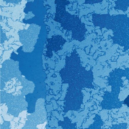
(a) 750 K                                 (b) 780 K                                  (c) 810 K

   100nm                                      100nm                                      100nm

Figure 1: STM images of nitrogen islands on ordered Cu3 Au(100) after 5 min of annealing at (a) 750 K (b) 780 K and (c) 810 K. The
images were acquire at a temperature of 1.5 K with constant current at (a) 0.1 nA and 0.2 V, (b) 0.1 nA and 1 V and (c) 0.4 nA and
0.2 V. The nitrogen islands appear as darker areas surrounded by brighter areas, which are bare Cu3 Au(100).

      (a) 780 K                                 (b) 840 K                                  (c) 870 K

   100nm                                      100nm                                      100nm

Figure 2: STM images of nitrogen islands on disordered Cu3 Au(100) after 5 min of annealing at (a) 780 K (b) 840 K and (c) 870 K. The
images were acquire at a temperature of 1.5 K with constant current at (a) 0.1 nA and 50 mV, (b) 0.2 nA and 100 mV and (c) 0.2 nA
and 50 mV.

tions. During measurements the pressure was                          filament, and extrapolate back.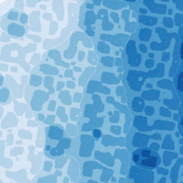
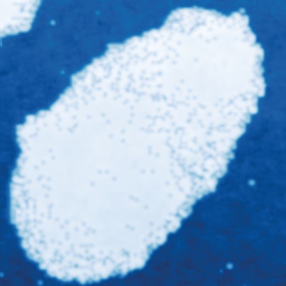
(a) 10 mV                                   (b) 1.5 V                                  (c) 4.5 V

Figure 3: STM images of a nitrogen islands on disordered Cu3 Au(100), scanned at a constant current of 0.5 nA and a bias of (a)
10 mV, (b) 1.5 V and (c) 4.5 V. The surface was annealed 5 min at 840 K after nitrogen sputtering. The insets are higher resolution
scans of a section of the nitrogen island taken at identical measurement parameters. The corresponding area on the island is indicated
by a white rectangle. For (a) and (b) the nitrogen islands are darker than the surrounding bare Cu3 Au(100). This contrast is inverted
for (c).

damage to the surface, we follow the sputtering by                       Figure 1 shows the effect of different annealing
an annealing process, leading to the formation of a                   temperatures (as determined via the process de-
c(2x2)N reconstruction on the Cu3 Au(100) surface,                    scribed above) on the size and distribution of the
similar to that reported for Cu(100) [2].                             islands. The resulting islands vary in size from
   A Cu3 Au crystal can be in two distinct phases:                    10 nm to 100 nm in their longest direction where
an ordered L12 phase [16, 17] upon annealing be-                      the largest islands appear only at a higher temper-
low a critical temperature Tc = 663 K [18, 19, 20],                   ature. We observe a trend towards larger islands
and a disordered phase above this temperature                         for higher temperatures. The edges of the island
[21, 22]. While both phases have the FCC crys-                        are mostly straight and oriented along the crystal-
tal structure, in the L12 phase the Au atoms are                      lographic axes (rotated between 5◦ and 10◦ clock-
periodically distributed over the crystal whereas in                  wise relative to the image frame), as is observed
the disordered phase they are not. The transition                     on Cu(100). The island size is strongly increased
between the two phases is reversible [23, 24]: the                    with respect to the case of Cu(100) owing to a re-
crystal can be brought back into the L12 phase in a                   duced strain accumulation, due to the better match
matter of hours by annealing at temperature near                      in lattice parameters.
Tc [23, 25]. The lattice constant of the disordered                      A second series of experiments was performed
phase is slightly larger than the ordered L12 phase                   after a prolonged high temperate treatment of the
(0.3762 nm and 0.3754 nm) respectively [26]).                         crystal. We annealed the crystal for 15 hours at
                                                                      >900 K. This temperature is well above the critical
                                                                      temperature of 663 K, driving the crystal from the
3. Results and discussions                                            ordered L12 into a disordered FCC phase.
                                                                         The disordered crystal was then prepared in a
   In a first series of experiments, a clean and or-                  similar fashion as the ordered crystal. The amount
dered L12 sample was sputtered with nitrogen for                      of sputtered nitrogen is similar to the amount sput-
45 s at a current of 0.8 µA and an accelerating volt-                 tered in the preparations in Figure 1 and the an-
age of 0.5 kV. The sample was then annealed                           nealing time was kept unchanged at 5 min for each
for 5 min. The annealing temperature was kept at                      preparation. The resulting surfaces at different an-
T > Tc for only short periods of time, preserving                     nealing temperatures can be seen in Figure 2.
the order in the bulk of the crystal. The surface                        The island sizes follow the same trend as on the
is faster to both order and disorder when crossing                    ordered crystal, with islands ranging from 10 nm
the critical temperature, taking place on a broader                   to 100 nm where larger islands are observed for
temperature range [27, 28].                                           higher temperatures. A major difference is found
                                                                  3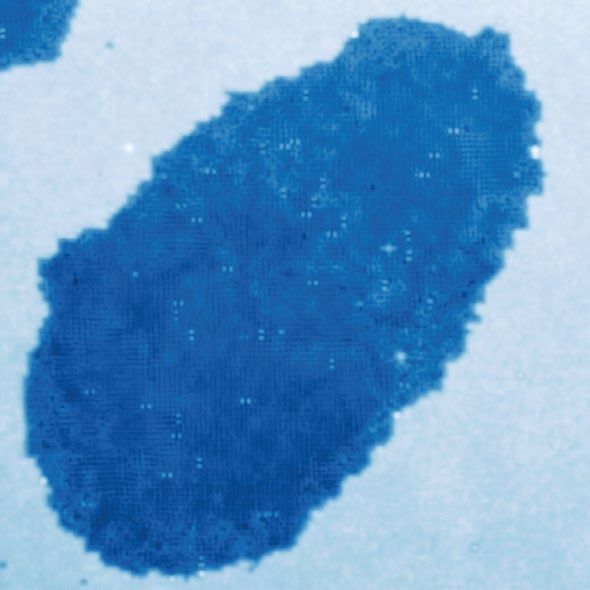
(a)                                                              (b)                             (c)
                               0.1V     1.5V

                                                                                                    5nm

                                                                                                     (d)

                                                                     50nm                           5nm

                                                                     (e)    Before scanning at 5V    (f)   After scanning at 5V

    200nm                                                            5nm                            5nm

Figure 4: (a) Nitrogen island with an area of over 145 000 nm2 with Fe adatoms evaporated onto it. (b-f) STM images of percolated
areas. The sample was annealed for (a,e,f) 15 min in three steps at 810 K, 780 K and 750 K, (b) 20 min at 930 K and (c,d) 20 min
at 870 K. The STM images were taken at (a) 0.2 nA and 100 mV (inset at 1.5 V), (b) 0.1 nA and 200 mV, (c) 0.1 nA and −20 mV, (d)
0.2 nA and 20 mV and (e, f) 0.1 nA and 100 mV. (e) and (f) show the same area before and after a scan of this area at 0.1 nA and 5 V.

in the island geometry. In the ordered case the is-                      The defect distribution gives us an indication on
lands have mostly straight edges. In contrast, the                    the formation and merging of islands. On round
islands of the disordered crystal are more rounded,                   islands, the defects are mostly around the edges,
showing no clear preferable orientation with re-                      where during growth new nitrogen joins the island
gards to the crystallographic directions, indicating                  and where the c(2 × 2) reconstruction is therefore
a more isotropic diffusion. This can be explained                     not completed. Due to Brownian movement, the is-
by disorder creating slight local variations in the                   lands diffuse on the surface and will eventually col-
lattice parameters and allowing the strain of the ni-                 lide. This process of coalescence is visible in Fig-
trogen reconstruction to be released. This strain                     ure 3, where two islands were frozen in the process
release process could allow the reconstruction of                     of merging. Longer annealing time or higher tem-
islands without fundamental limits in their sizes.                    perature would allow the island to properly merge
   Scanning the surface at higher bias voltage Vb                     and adopt a round shape. This establishes a clear
reveals features that were not evident for Vb <                       relation between the elongation of the islands and
0.5 V. Figure 3 shows the same island scanned at                      the coalescence between multiple islands.
different bias voltages. At Vb = 1.5 V we observe                        Raising the annealing temperature allows for
bright spots appearing in the nitrogen reconstruc-                    faster dynamics, accelerating the island merging
tion. At Vb = 10 mV and with atomic resolution,                       process which consequently leads to larger and
we can see that those bright spots correspond-                        rounder islands. Figure 4a shows a ∼145 000 nm2
ing to defects in the nitride lattice (see insets of                  island observed on the disordered crystal. The to-
Figure 3). The exact nature those defects is un-                      tal area of this island is an improvement of three
known, but they were observed only in the disor-                      orders of magnitude respect to the maximum area
dered phase. We suggest that they are Au atoms                        of a nitrogen islands on Cu(100) [12]. However, in
that are incorporated into the copper-nitride layer                   the inset of Figure 4a, taken at higher bias, we can
as substitutions of Cu atoms. In the L12 phase, ev-                   observe a high density of defects on the nitrogen
ery other layer in the (100) direction consists exclu-                reconstruction evenly distributed along the island,
sively of Cu atoms; after saturation with nitrogen,                   suggesting a higher Au-Cu substitution at the sur-
the surface is terminated on a Cu-only layer [13].                    face at elevated growth temperatures. Nonethe-
                                                                 4
(a) (a)
20mV 1.5V
Clean metal and islands
Cu3Au
5nm N/Cu3Au
(b)
(c)
Percolated surface
20nm
(d) (b)
N/Cu3Au
5nm
Cu3Au
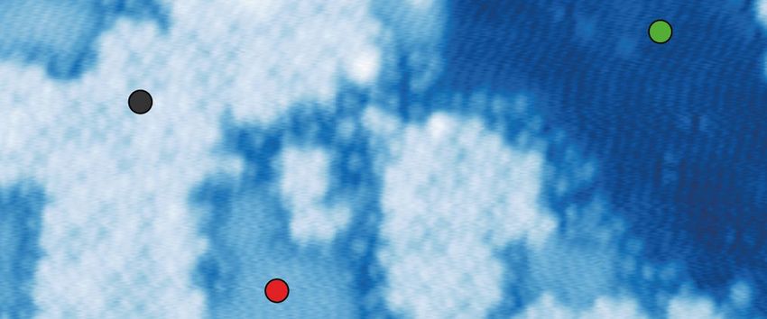
Figure 5: Tunneling specstroscopy measurements on regular
and percolated areas. (a) STM image of a regular nitrogen is- Figure 6: (a) 1 × 5 and 2 × 4 structures of Fe atoms similar
land on disordered Cu3 Au. (b,c) dI/dV spectroscopy measure- to [7] assembled through vertical manipulation on a ∼5000 nm2
ments at constant current, taken at different positions on regular nitrogen island on Cu3 Au. (b) dIdV spectroscopy measure-
(b) and percolated (c) areas. Measurement locations are indi- ments taken on each of the atoms of a 1 × 3 Fe structure built
cated with corresponding colours in (a) and (d). (d) STM image on an island of similar size as in (a). Spectroscopy was taken
taken in a percolated area. STM scans were taken at 1.5 K in the center of each atom with initial settings of 800 pA and
and (a) 100 pA and 20 mV (inset at 1.2 V) and (d) 200 pA and −20 mV. All structures were built on the same sample, which
100 mV. was annealed at 810 K, 780 K and 750 K for 5 min at each tem-
perature. The STM images were taken at (a) 50 pA and 20 mV
and (b) 200 pA and 50 mV.
less, we successfully evaporated and manipulated
Fe atoms and on this island (white dots), and were
able to engineer well-behaved spin structures (see sample surface, indicating that various phases can
Figure 6). coexist on a single crystal. By starting the anneal-
The area surrounding this island presents an ing at a higher temperature and gradually lowering
irregular topography, highlighted in Figure 4c-e, the temperature, we are able to create round large
which we will denote as percolation regions. We islands with smooth nitrogen reconstruction, where
observe this kind of behaviour for the prepara- the defects are mostly on the edges.
tions we performed at highest temperatures. They Figure 5 shows constant current dI/dV spec-
consist of a square pattern broken up by irreg- troscopy measurements on both regular and per-
ular channels connecting larger islands, as well colated areas. As seen in Figure 5b, the nitride
as clean patches of exposed Cu3 Au surface. We islands in the regular region behave analogously
have seen the percolation region to be unstable for to those reported for Cu(100) [29]. In the perco-
Vb > 4 V both while scanning (see Figure 4e, f) and lated region (Figure 5c,d), three distinct phases are
during spectroscopy (see Figure 5). observed: two that behave similarly to the regular
We note that on the same sample preparation, region (red, green) and the phase with the square
it is possible to observe areas in the percolation pattern (black), where the spectroscopy is mostly
regime and areas with regular nitride islands by featureless (apart of its instability).
macroscopically displacing the STM tip accros the The nitrogen islands on Cu3 Au(100) are suitable
5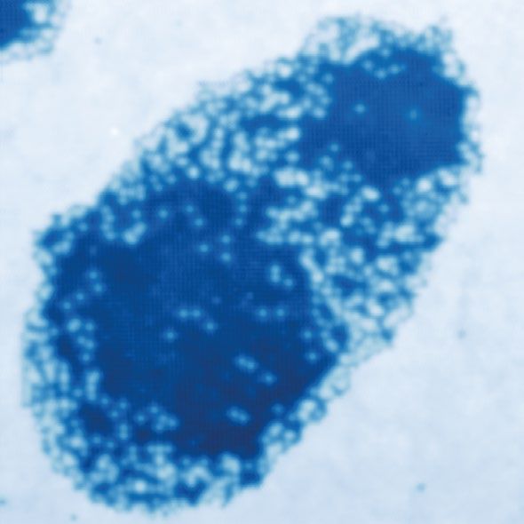
for adatom manipulation. We assembled many                             [3] C. F. Hirjibehedin, C. P. Lutz, A. J. Heinrich, Spin Coupling
structures of Fe adatoms — from dimers to longer                           in Engineered Atomic Structures, Science 312 (5776)
                                                                           (2006) 1021–1024.
chains and blocks. Examples of such successfully                       [4] C. F. Hirjibehedin, C.-Y. Lin, A. F. Otte, M. Ternes,
assembled structure can be seen in Figure 6a. In                           C. P. Lutz, B. A. Jones, A. J. Heinrich, Large Magnetic
Figure 6b we show spectroscopy measurements                                Anisotropy of a Single Atomic Spin Embedded in a Sur-
on the three atoms of a Fe trimer, which are quan-                         face Molecular Network, Science 317 (5842) (2007) 1199–
                                                                           1203.
titatively the same as for a trimer assembled on ni-                   [5] B. Bryant, A. Spinelli, J. J. T. Wagenaar, M. Gerrits, A. F.
tride on Cu(100) [30]. Atomic manipulation is per-                         Otte, Local Control of Single Atom Magnetocrystalline
formed vertically, by moving an atom from the sur-                         Anisotropy, Phys. Rev. Lett. 111 (12) (2013) 127203.
face to the tip and subsequently form the tip to the                   [6] A. Spinelli, M. Gerrits, R. Toskovic, B. Bryant, M. Ternes,
                                                                           A. F. Otte, Exploring the phase diagram of the two-impurity
surface on the desired position [3].                                       Kondo problem, Nature Communications 6 (2015) 10046.
                                                                       [7] S. Loth, S. Baumann, C. P. Lutz, D. M. Eigler, A. J. Hein-
                                                                           rich, Bistability in Atomic-Scale Antiferromagnets, Science
4. Conclusion                                                              335 (6065) (2012) 196–199, 00316.
                                                                       [8] A. Spinelli, M. P. Rebergen, a. A. F. Otte, Atomically crafted
   We have studied the growth of c(2 × 2) nitride                          spin lattices as model systems for quantum magnetism,
                                                                           Journal of Physics: Condensed Matter 27 (24) (2015)
islands on the Cu3 Au(100) crystal surface, which                          243203, 00005.
results in island sizes that are much larger than                      [9] R. Toskovic, R. van den Berg, A. Spinelli, I. S. Eliens,
on the well-studied Cu(100) surface. When the                              B. van den Toorn, B. Bryant, J.-S. Caux, A. F. Otte, Atomic
crystal is prepared in the ordered phase, we ob-                           spin-chain realization of a model for quantum criticality,
                                                                           Nat Phys 12 (7) (2016) 656–660.
serve mostly rectangular nitride islands, which in-                   [10] D.-J. Choi, R. Robles, S. Yan, J. A. Burgess, S. Rolf-
crease in size with temperature. On the disordered                         Pissarczyk, J.-P. Gauyacq, N. Lorente, M. Ternes, S. Loth,
phase we see a similar relation between annealing                          Building complex Kondo impurities by manipulating entan-
                                                                           gled spin chains, Nano Lett.
temperature and island size, but in this case the
                                                                      [11] F. E. Kalff, M. P. Rebergen, E. Fahrenfort, J. Girovsky,
islands are round, indicating that effects of strain                       R. Toskovic, J. L. Lado, J. Fernández-Rossier, A. F. Otte,
due to lattice mismatch have diminished. Measure-                          A kilobyte rewritable atomic memory, Nat Nano 11 (11)
ments at higher voltages reveal defects, the distri-                       (2016) 926–929.
                                                                      [12] J. C. Oberg, M. R. Calvo, F. Delgado, M. Moro-Lagares,
bution of which gives information about the coales-                        D. Serrate, D. Jacob, J. Fernández-Rossier, C. F. Hir-
cence of islands during growth. The nitride islands                        jibehedin, Control of single-spin magnetic anisotropy by
on Cu3 Au(100) are found to be equally suitable for                        exchange coupling, Nature Nanotechnology 9 (1) (2014)
vertical manipulation of magnetic adatoms as their                         64–68.
                                                                      [13] H. Niehus, C. Achete, Surface structure investigation of
counterparts on Cu(100).                                                   nitrogen and oxygen on Cu3Au(100), Surface Science
                                                                           289 (1) (1993) 19–29.
                                                                      [14] T. Choi, C. D. Ruggiero, J. A. Gupta, Incommensurability
5. Acknowledgements                                                        and atomic structure of c2x2 N/Cu100: A scanning tunnel-
                                                                           ing microscopy study, Phys. Rev. B 78 (3) (2008) 035430.
    We thank P. N. First for discussions and R.                       [15] W. P. Davey, Precision Measurements of the Lattice Con-
                                                                           stants of Twelve Common Metals, Phys. Rev. 25 (6) (1925)
Toskovic, as well as A. M. Koning and J. W. van                            753–761.
Dam for preliminary studies. This work was sup-                       [16] Z. W. Lu, S.-H. Wei, A. Zunger, Electronic structure of or-
ported by the Netherlands Organisation for Scien-                          dered and disordered Cu3Au and Cu3Pd, Phys. Rev. B
tific Research (NWO) and by the European Re-                               45 (18) (1992) 10314–10330.
                                                                      [17] R. Oguma, T. Eguchi, S. Matsumura, S. K. Son, Domain
search Council.                                                            growth and off-phase boundary structures in L12-type or-
                                                                           dering, Acta Materialia 54 (6) (2006) 1533–1539.
                                                                      [18] T. M. Buck, G. H. Wheatley, L. Marchut, Order-Disorder
6. References                                                              and Segregation Behavior at the Cu3Au(001) Surface,
                                                                           Phys. Rev. Lett. 51 (1) (1983) 43–46.
References                                                            [19] V. S. Sundaram, R. S. Alben, W. D. Robertson, The order-
                                                                           disorder transformation at a (100) surface of Cu3Au, Sur-
 [1] A. Spinelli, B. Bryant, F. Delgado, J. Fernández-Rossier,             face Science 46 (2) (1974) 653–671.
     A. F. Otte, Imaging of spin waves in atomically designed         [20] C. Mannori, G. Boato, M. Canepa, P. Cantini, L. Mattera,
     nanomagnets, Nat Mater 13 (8) (2014) 782–785.                         S. Terreni, Surface vs. bulk order/disorder transition in a
 [2] F. M. Leibsle, S. S. Dhesi, S. D. Barrett, A. W. Robinson,            binary alloy. A He diffraction study of the Cu3Au(001) sur-
     STM observations of Cu(100)-c(2x2)N surfaces: Evidence                face, Europhysics Letters (EPL) 45 (6) (1999) 686–692.
     for attractive interactions and an incommensurate c(2x2)         [21] D. G. Morris, F. M. C. Besag, R. E. Smallman, Ordering
     structure, Surface Science 317 (3) (1994) 309–320.                    and disordering in Cu3Au, The Philosophical Magazine: A

                                                                  6
Journal of Theoretical Experimental and Applied Physics
       29 (1) (1974) 43–57.
[22]   K. D. Jamison, D. M. Lind, F. B. Dunning, G. K. Walters, Po-
       larized LEED investigation of the order/disorder transition
       at a Cu3Au(100) surface, Surface Science 159 (2) (1985)
       L451–L459.
[23]   D. T. Keating, B. E. Warren, Long-Range Order in Beta-
       Brass and Cu3Au, Journal of Applied Physics 22 (3)
       (1951) 286–290.
[24]   A. Benisek, E. Dachs, The vibrational and configurational
       entropy of disordering in Cu3Au, J Alloys Compd 632
       (2015) 585–590.
[25]   S. Katano, M. Iizumi, Y. Noda, Lattice dynamics of Cu3 Au
       in the ordered and disordered states, Journal of Physics
       F: Metal Physics 18 (10) (1988) 2195–2202.
[26]   T. P. Moffat, F.-R. F. Fan, A. J. Bard, Electrochemical and
       Scanning Tunneling Microscopic Study of Dealloying of
       Cu3Au, J. Electrochem. Soc. 138 (11) (1991) 3224–3235.
[27]   V. S. Sundaram, B. Farrell, R. S. Alben, W. D. Robert-
       son, Order-Disorder Transformation at the (100) Surface
       of Cu3Au, Phys. Rev. Lett. 31 (18) (1973) 1136–1139.
[28]   L. Houssiau, P. Bertrand, Order-disorder phase transition
       of the Cu3Au(100) surface studied by ToF-ion scattering,
       Nuclear Instruments and Methods in Physics Research
       Section B: Beam Interactions with Materials and Atoms
       118 (1) (1996) 467–472.
[29]   T. Choi, C. D. Ruggiero, J. A. Gupta, Tunneling spec-
       troscopy of ultrathin insulating Cu2N films, and single Co
       adatoms, Journal of Vacuum Science & Technology B:
       Microelectronics and Nanometer Structures Processing,
       Measurement, and Phenomena 27 (2) (2009) 887–890.
[30]   S. Yan, D.-J. Choi, J. A. J. Burgess, S. Rolf-Pissarczyk,
       S. Loth, Control of quantum magnets by atomic exchange
       bias, Nature Nanotechnology 10 (1) (2015) 40–45.

                                                                      7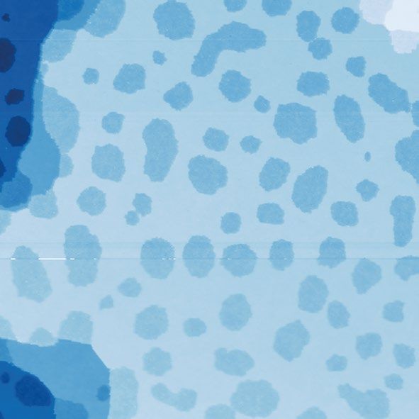
You can also read