FIELD-INDUCED RESISTANCE PEAK IN A SUPERCONDUCTING NIOBIUM THIN FILM PROXIMITY COUPLED TO A SURFACE RECONSTRUCTED SRTIO3 - NATURE
←
→
Page content transcription
If your browser does not render page correctly, please read the page content below
www.nature.com/npjquantmats

                  ARTICLE                 OPEN

                  Field-induced resistance peak in a superconducting niobium
                  thin film proximity coupled to a surface reconstructed SrTiO3
                  Akhilesh Kr. Singh1, Uddipta Kar1,2, Matthew D. Redell3, Tsung-Chi Wu1, Wei-Hsiang Peng1, Bipul Das1, Satish Kumar1,
                  Wei-Cheng Lee 3 ✉ and Wei-Li Lee 1 ✉

                      Oxygen vacancy is known to play an important role for the physical properties in SrTiO3(STO)-based systems. On the surface, rich
                      structural reconstructions had been reported owing to the oxygen vacancies, giving rise to metallic surface states and unusual
                      surface phonon modes. More recently, an intriguing phenomenon of a huge superconducting transition temperature enhancement
                      was discovered in a monolayer FeSe on STO substrate, where the surface reconstructed STO (SR-STO) may play a role. In this work,
                      SR-STO substrates were prepared via thermal annealing in ultra-high vacuum followed by low energy electron diffraction analyses on
                      surface structures. Thin Nb films with different thicknesses (d) were then deposited on the SR-STO. The detailed studies of the
                      magnetotransport and superconducting property in the Al(1 nm)/Nb(d)/SR-STO samples revealed a large positive magnetoresistance
                      and a pronounced resistance peak near the onset of the resistive superconducting transition in the presence of an in-plane field.
                      Remarkably, the amplitude of the resistance peak increases with increasing fields, reaching a value of nearly 57% of the normal state
                      resistance at 9 T. Such resistance peaks were absent in the control samples of Al(1 nm)/Nb(d)/STO and Al(1 nm)/Nb(d)/SiO2.
1234567890():,;

                      Combining with DFT calculations for SR-STO, we attribute the resistance peak to the interface resistance from the proximity coupling
                      of the superconducting niobium to the field-enhanced long-range magnetic order in SR-STO that arises from the spin-polarized in-
                      gap states due to oxygen vacancies.
                      npj Quantum Materials (2020)5:45 ; https://doi.org/10.1038/s41535-020-0242-4

                  INTRODUCTION                                                                           resistance peak was uncovered at temperatures near the onset
                  One intriguing factor governing the physical property in an oxide                      of the superconductivity in niobium, which is absent in zero field
                  system is the oxygen content. In cuprates, extensive studies have                      and also in control samples of niobium films deposited either on
                  demonstrated the effective tuning of the superconducting                               SiO2/Si substrate or on TiO2-terminated STO without any surface
                  properties by simply varying the oxygen content in the parent                          reconstruction. Surprisingly, the magnitude of resistance peak is
                  compounds1–3. On the other hand, it is also known that oxygen                          more pronounced with in-plane fields and appears to grow with
                  vacancies in SrTiO3 (STO) serve as electron donors4, which turns                       increasing field strength. The DFT calculations were carried out
                  the STO from a wide band-gap insulator into an unusual dilute                          using oxygen vacancy structures obtained from the LEED analysis,
                  superconductor5. As it turns out, the influence of the oxygen                           where a unique spin-polarized in-gap states was found. The peak
                  vacancies to STO can be multifold according to some recent                             resistance phenomenon in Nb/SR-STO is likely resulting from the
                  investigations6–8. Microscopically, oxygen vacancies locally break                     interplay between the superconducting Nb and the magnetism
                  the d-orbital symmetry of titanium ions, giving rise to unusual in-                    from the spin-polarized in-gap states of SR-STO.
                  gap states and possible magnetism. Such in-gap states in oxygen-
                  deficient STO have been observed in angle resolved photo-
                  emission spectroscopy and scanning tunneling spectroscopy                              RESULTS
                  measurements9,10. More recently, a remarkable and nearly 10-                           For more than ten TiO2-terminated STO substrates we prepared,
                  fold enhancement of superconducting transition temperature was                         several annealing temperatures ranging from 800 °C to 900 °C
                  discovered in a monolayer of FeSe on STO11, which motivates                            were used with an annealing time of 4 h, and those substrates
                  numerous investigations to reveal the intrinsic mechanism for                          were then cooled down to room temperature for the LEED
                  such a huge Tc enhancement12,13. Among various possibilities,                          characterizations. The LEED pattern transformed from a simple
                  oxygen vacancy and charge transfer from STO substrate are                              cubic structure of major diffraction spots (Fig. 1a) into a much
                  potential factors14, and more experimental efforts are keenly                          more complex pattern with additional secondary diffraction spots
                  required. In light of this quest, we study the influence of the                         that come from the surface structural reconstruction effect. We
                  superconducting property in thin niobium (Nb) films deposited on                        also note that the diffraction spots become broader with different
                  surface reconstructed STO (SR-STO) substrates. The SR-STO                              intensity after UHV annealing, indicating an increase in the surface
                  substrate can be prepared by annealing TiO2-terminated STO in                          roughness and also the inelastic scattering contribution to the
                  an ultra-high vacuum (UHV) environment, and the resulting                              LEED pattern. A rich variety of surface structure on STO after UHV
                  oxygen vacancies cause structural reconstruction at the STO                            annealing has been reported previously by many authors15–17,
                  surface that can be identified by low energy electron diffraction                       where annealing temperature and duration are both crucial
                  (LEED) measurement and analysis. A striking field-induced                               factors. For the following Al(1 nm)/Nb(d)/SR-STO sample

                  1
                   Institute of Physics, Academia Sinica, Nankang, Taipei 11529, Taiwan. 2Nano Science and Technology, Taiwan International Graduate Program, Academia Sinica and National
                  Taiwan University, Nankang, Taiwan. 3Department of Physics Applied Physics, and Astronomy, Binghamton University, Binghamton, NY 13902, USA. ✉email: wlee@binghamton.edu;
                  wlee@phys.sinica.edu.tw

                  Published in partnership with Nanjing University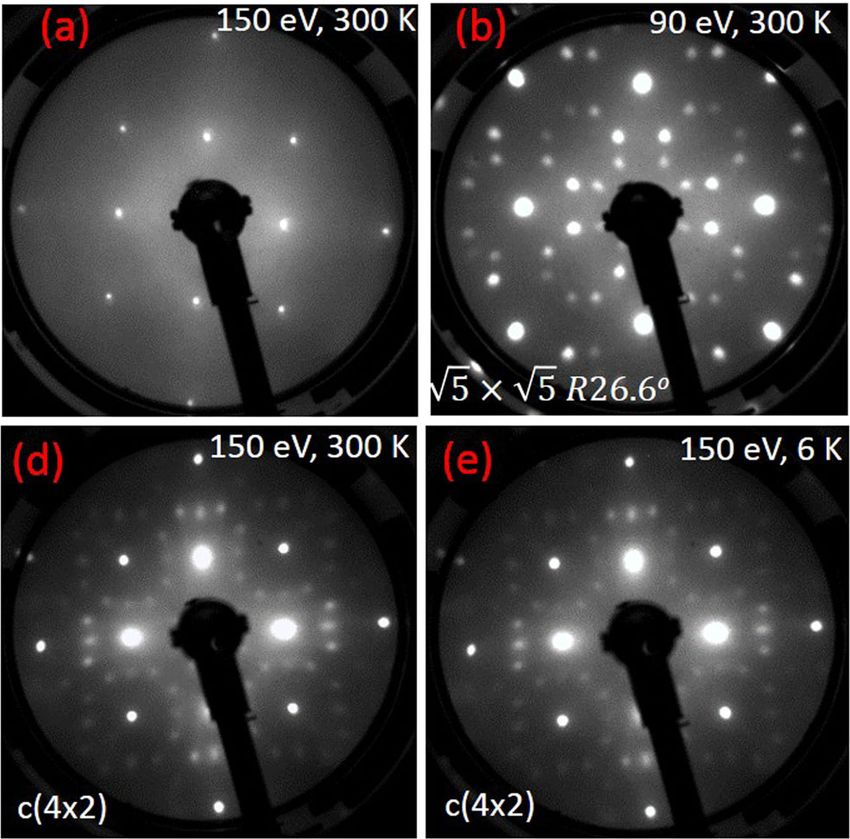
A.Kr. Singh et al.
                  2

                      Fig. 1 The surface structurepffiffiffi of p
                                                          SR-STO.  The LEED patterns of TiO2-terminated STO(100) substrates at room temperature: a no surface
1234567890():,;

                                                            ffiffiffi
                      structural reconstruction. b 5 ´ 5R26.6°   pffiffisurface
                                                                    ffi pffiffiffi structure after UHV annealing. d c(4 × 2) surface structure after UHV annealing. c, f are the
                      simulated LEED patterns based on the 5 ´ 5 R26.6° and c(4 × 2) surface structures, respectively, showing excellent agreements with
                      observed LEED patterns. The red and blue circles represent the secondary diffraction spots from different surface structure domains. Those
                      surface structures after UHV annealing are stable after cooling down to lower temperatures. e shows the LEED pattern at 6 K, which is identical
                      to that with c(4 × 2) surface structure at room temperature.

                      preparations, we chose to use the annealing temperature of                  2b plots the normalized sheet resistance Rs/Rn versus T near the
                      850 °C and annealing time of 4 h for the preparation of all SR-STO          superconducting transition for samples with d = 10 nm. We
                      substrates. With this annealing condition, two distinct and                 adopted the convention by taking the superconducting transition
                      reproducible surface structures
                                                   pffiffiffi can
                                                          pffiffiffi be identified from the LEED         temperature Tc as the temperature with Rs/Rn = 1/2. The Tc equals
                      measurements. They are 5 ´ 5 R26.6° structure and c(4x2)                    4.6 K and 4.9 K for Sub. = STO (blue line in Fig. 2b) and Sub. = SiO2/
                      structure, which are shown in Fig. 1b and d, respectively.  pffiffiffi The
                                                                                         pffiffiffi     Si (red line), while Tc for Sub. = SR-STO (black line) is apparently
                      simulated LEED patterns using LEEDpat package18 with 5 ´ 5                  higher with a value of 6.2 K. The detailed thickness dependence on
                      R26.6° and c(4 × 2) structures, shown in Fig. 1c and f, respectively,       the Tc is shown in Fig. 2c, where the Nb thickness was in-situ
                      are in excellent agreements with the patterns we observed. The              monitored by a quartz crystal microbalance. The control samples of
                      red and blue circles are secondary diffraction spots, deriving from         Sub. = SiO2/Si with different thicknesses follow a simple relation of
                      different surface structure domains. We also note that those                log(Tc) ∝ 1/d, which is consistent with some earlier works19. We
                      surface structures of SR-STO are stable down to lower tempera-              remark that samples of Sub. = SR-STO (star symbols and open
                      tures. Fig. 1f is an example of the LEED pattern of c(4 × 2) structure      triangles in Fig. 2c) turn out to show higher Tc compared to control
                      measured with SR-STO at 6 K, showing negligible changes as                  samples (circles and diamonds) with the same Nb thickness, where
                      compared to that at room temperature (Fig. 1d).                             the difference in Tc appears to be larger for thinner Nb layer
                         In order to study the influence of the proximity coupling                 (smaller d).
                      between SR-STO and the superconducting Nb layer, control                       The upper critical field Hc2 can be readily obtained from the
                      samples using different substrates of SiO2/Si and STO were                  field dependence of sheet resistance Rs(H) and Hall resistance
                      fabricated for comparison. The sample composition is illustrated in         Rxy(H) at temperatures ranging from 2 K to 7 K as shown in Fig. 3a
                      the lower inset cartoon of Fig. 2a. Figure 2a shows the                     for Al(1 nm)/Nb(10 nm)/SR-STO sample with a field perpendicular
                      temperature dependence of the sheet resistance Rs for Al(1 nm)/             to the film surface. The extracted Hc2 as a function of the reduced
                      Nb(10 nm)/Sub. with Sub. = STO, SiO2/Si and SR-STO. The sheet               temperature (T/Tc) is shown as black squares in Fig. 3b, where the
                      resistance Rs equals 96.2 Ω and 77.8 Ω at T = 280 K for Sub. = STO          results for control samples of Sub. = STO (blue circles) and SiO2/Si
                      and SiO2/Si, respectively, which is nearly 8-fold larger than that in       (red diamonds) were also included for comparison. For Sub. = SR-
                      sample with Sub. = SR-STO (Rs ≈ 12.2 Ω). In particular, Rs drops            STO at T/Tc ≈ 0.4, μ0Hc2,⊥ (H ⊥ ab) and μ0Hc2,∥ (H ∥ ab) equal 2.24 T
                      rapidly with decreasing temperature for Sub. = SR-STO, giving a Rs          and 10.88 T, respectively. The effective superconducting layer
                      of about 12 mΩ at T = 10 K, which is more than three orders of              thickness dGL and also zero temperature Ginzburg-Landau (GL)
                      magnitude lower than that in Sub. = STO and SiO2/Si at similar              superconducting coherence length ξGL(0) can be estimated from
                      temperature. Such a low Rs at lower temperatures in Sub. = SR-              the Hc2 anisotropy based on the GL theory of μ0 Hc2;k ¼
                      STO indicates a highly conducting nature in the SR-STO, and the                pffiffi         qffiffiffiffiffiffiffiffiffiffiffiffi
                                                                                                        3Φ0
                      electron–phonon scattering plays a crucial role, giving rise to a           d GL πξ GL ð0Þ  1  TTc and μ0 Hc2;? ¼ 2πξΦ2 0 ð0Þ ð1  TTc Þ20, where Φ0 is the
                                                                                                                                            GL
                      rapid drop of more than three orders of magnitude in Rs as                  flux quantum. The extracted dGL and ξGL(0) values are summarized
                      temperature goes from 300 K to 10 K. Therefore, Al(1 nm)/Nb                 in Table 1. For Sub. = SR-STO and d = 10 nm, effective thickness d
                      (10 nm)/SR-STO shall be considered as an interesting system of              is about 8.5 nm that is about 10% lower than that for control
                      superconducting layer proximity coupled to a highly-conducting              samples. On the other hand, ξ(0) equals 9.3 nm, which is about
                      SR-STO substrate with a strong electron–phonon coupling. Figure             10% higher than that for control samples. Similar behavior is

                      npj Quantum Materials (2020) 45                                                                        Published in partnership with Nanjing University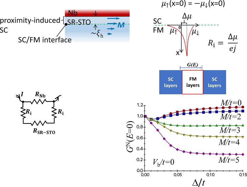
A.Kr. Singh et al.
                                                                                                                                                  3

Fig. 2 The sheet resistance data. a The temperature dependence of the sheet resistance Rs in a logarithmic scale for Al(1 nm)/Nb(10 nm)/Sub.
with three different substrates of STO, SiO2/Si, and SR-STO. For Sub. = SR-STO, Rs is nearly an order of magnitude smaller at room temperature,
and it rapidly decreases with decreasing temperature, giving a mere Rs ≈ 10 mΩ at around 10 K. The inset cartoon of a illustrates the device
composition. b The normalized sheet resistance Rs/Rn as a function of temperature below 7 K. The blue and red lines are the curves for Al
(1 nm)/Nb(10 nm)/STO and Al(1 nm)/Nb(10 nm)/SiO2/Si samples, respectively, showing lower superconducting transition temperatures as
compared to that in Al(1 nm)/Nb(10 nm)/SR-STO. c The superconducting transition temperature Tc in log scale versus 1/d, where d is the
thickness of the Nb layer. The phenomenological dependence of log (Tc) ∝ 1/d is well observed in samples with Sub. = SiO2/Si. Tc appears to
be higher in samples with Sub. = SR-STO (star symbols and open triangles).

found in d = 15 nm samples. We do note that dGL values are close         (circles) and H ∥ ab ⊥ I (squares) are summarized in Fig. 4c, where
to but somewhat smaller than the nominal thickness d                     the inset figure of Fig. 4c illustrates the definitions of the Ton, Tp,
determined from the quartz crystal microbalance. The magne-              and Δr we used in the discussions. In general, Δr is zero at low
toresistance (MR) data of Al(1 nm)/Nb(10 nm)/Sub. are shown in           fields, and it starts to appear above a certain field, where Δr grows
Fig. 3c with green and black lines for transverse MR (H ⊥ ab) and        practically linear with field strength up to more than 10 T. Δr can
longitudinal MR (H ∥I ), respectively. A large positive transverse       be as large as 0.56 at μ0H = 8.5 Tesla for d = 15 nm with H ∥ ab ⊥ I.
and longitudinal MR with a magnitude of 251% and 86%,                    In the sample of d = 15 nm with H ∥ I, we note that Δr decreases
respectively, at μ0H = 10 T are observed in the sample with Sub. =       with increasing field for 5 ≤ μ0H ≤ 7.5 T, where the corresponding
SR-STO (left panel of Fig. 3c), which is more than two orders of         Tp turns out to shift to a lower temperature (see Supplementary
magnitude larger than that in samples with Sub. = SiO2/Si (middle        Fig. 1), and thus the peak resistance effect was largely reduced by
panel) and Sub. = STO (right panel). We also remark that the             the rapid drop in Rs at Tc. From those observations, we
negative Hall slope in sample with Sub. = SR-STO (Fig. 3a lower          constructed a unique H–T phase diagram for the proximity
panel at 7 K) indicates dominant electron-like carriers, which is        coupled superconducting system of Al(1 nm)/Nb(d)/SR-STO, which
opposite to the hole-like carriers found in control samples with         is shown in Fig. 4d for d = 10 nm with H ∥ I. The color code in
Sub. = STO and SiO2/Si (see Supplementary Fig. 2).                       Fig. 4d corresponds to the value of normalized sheet resistance of
    As shown in Fig. 3b, the upper critical field Hc2 for H ∥ I can be    Rs/Rn. Other than the regular phase boundary of Tc (yellow line)
more than 10 Tesla at lower temperatures. An unusual field-               between the normal state (light gray color) and superconducting
induced resistance peak was uncovered near the superconducting           state (black color), there is a white region between the Ton (blue-
transition, which is absent in zero field and tends to grow larger in     dashed line) and Tc lines, representing the appearance of unique
magnitude with field strength. Fig. 4a shows the Rs − H curves at         peak resistance effect. The Tp line is found to be close to Tc line at
temperature varying from 2 K to 7 K, where the inset cartoon             higher fields. It gradually moves toward the Ton line as H reduces
illustrates the field orientation of H ∥ I. For T ≤ 5 K, a pronounced     and meets with Ton line at about μ0H = 2.5 T, below which the
resistance peak was observed when the system passes from a               peak resistance effect completely disappears.
superconducting state to a normal state via field sweeping, and
the magnitude of resistance peak grows with increasing field
strength. On the other hand, such a resistance peak can also be          DISCUSSION
observed by temperature sweeping across the superconducting              Similar resistance peak phenomena have been reported before in
transition as shown in Fig. 4b with field ranging from 0 T to 12 T.       several systems, such as mesoscopic superconducting nanowires,
For μ0H ≥ 2.5 T, Rs starts to rise up as the temperature drops below     disordered superconductors, and anisotropic superconducting
an onset temperature (Ton), and it then reaches a local maximum          systems. A large resistance peak was observed at zero field in
at Tp before quickly entering the superconducting state with             several cuprates, including La2−xSrxCuO4, Bi2Sr2CaCu2O8, and
vanishing Rs. The relative magnitude of the resistance peak (Δr) for     YBa2Cu3O721–23, which has been attributed to either the interplane
Al(1 nm)/Nb(d)/SR-STO with d = 10 nm (open symbols) and 15 nm            vortex effect or the resistivity and thus Tc anisotropy in those
(closed symbols) with two different field geometries of H ∥ I             layered superconductors. Simulations, based on the measured

Published in partnership with Nanjing University                                                           npj Quantum Materials (2020) 45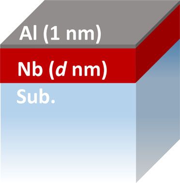
A.Kr. Singh et al.
4

    Fig. 3 The magneto-transport data. The upper and lower panels of a show the field dependence of the sheet resistance Rs and Hall
    resistance Rxy, respectively, in Al(1 nm)/Nb(10 nm)/SR-STO sample at temperature varying from 2 K to 7 K. The field is applied perpendicular to
    the film surface as illustrated in the inset figure of the lower panel. b The field anisotropy of upper critical field Hc2 as a function of reduced
    temperature T/Tc for samples using different substrates of SR-STO, SiO2/Si, and STO. c A comparison of the magnetoresistance (MR) in the
    normal state. The green and black lines are the MR curves with field perpendicular to the film surface and field parallel to the in-plane current
    direction, respectively. A large positive MR was observed in the sample with Sub. = SR-STO (left panel), which is more than two orders of
    magnitude larger than that with Sub. = SiO2/Si (middle panel) and Sub. = STO (right panel).

                                                                                 field and grows larger with field intensity as shown in Fig. 4c. The
     Table 1.   The GL parameters for Al(1 nm)/Nb(d)/Sub. samples.
                                                                                 fact that the resistance peak is much more pronounced with in-
                    d = 10 nm                     d = 15 nm                      plane fields also precludes the role of vortex effect. A number of
                                                                                 reports also showed pronounced resistance peaks at zero field in
    Sub.            dGL(nm)       ξGL(0)(nm)      dGL(nm)        ξGL(0)(nm)      disordered or granular superconductors27,28, where a possible
                                                                                 localized Cooper pair state due to disorder is proposed. This is
    SR-STO          8.5           9.3             10.1           9.2
                                                                                 incompatible to the absence of the resistance peak in zero field
    STO             9.5           8.6             11.0           8.1             found in our Nb/SR-STO samples. In addition, the atomic force
    SiO2            9.3           8.4             10.5           8.0             microscope and low angle reflectivity measurements reveal a
                                                                                 relatively smooth surface and a macroscopic uniformity of our Nb
                                                                                 film thickness, respectively (see supplementary Fig. 5). Therefore,
    difference in resistivity and Tc with a current either along or              disordered effect is less likely to be important in our Nb/SR-STO
    perpendicular to the layer, do reproduce such a resistance peak              samples, and other new mechanism is needed to explain the
    feature in the R–T curve24. We thus performed a control                      resistance peak phenomenon found in our Nb/SR-STO system.
    experiment by measuring the R–T behavior in Nb/SR-STO samples
    with currents applied along two different substrate crystalline
    axes. The difference in Tc and transition width is negligible, and we        DFT calculations of electronic structure of SR-STO
    thus exclude the possibility of field-induced in-plane anisotropy             A similar behavior was reported in mesoscopic devices, compris-
    for the occurrence of resistance peak. We also note that the                 ing superconducting electrodes proximity coupled by a ferromag-
    resistance peak we observed in Nb/SR-STO is not likely due to an             netic nanowire29. The resistance peak was found to survive under
    inhomogeneous current distribution, since the R–T profiles can be             intense magnetic field, and the magnetism in the ferromagnetic
    well reproduced regardless of the voltage leads geometry and                 wire was inferred to play a crucial role. In systems with a single
    location (see Supplementary Fig. 3 and Fig. 4). On the other hand,           oxygen vacancy, previous DFT results have shown that the
    resistance peak in a mesoscopic superconducting wire is typically            interplay between the local C4 symmetry breaking on Ti atom near
    associated with the formation of superconductor-normal metal-                the oxygen vacancy and the Hubbard U interaction leads to in-gap
    superconductor (SNS) junction and possible enhanced phase-                   states with local moments and a Rashba-like spin texture6–8.
    slips25,26. In this case, the resistance peak appears to be the largest      Furthermore, it has been reported that DFT with dynamical mean-
    in zero field, and its magnitude got suppressed rapidly by a small            field theory (DMFT) predicts strong tendency toward ferromag-
    external fields. This is the opposite of what we observed in our Nb/          netic ordering in the presence of two oxygen vacancies. In light of
    SR-STO samples, in which the resistance peak is absent in zero               this result, we performed DFT calculations using the Perdew-

    npj Quantum Materials (2020) 45                                                                    Published in partnership with Nanjing University
A.Kr. Singh et al.
5
Fig. 4 The peak resistance effect. a The field dependence of Rs at temperatures ranging from 2 K to 7 K in Al(1 nm)/Nb(10 nm)/SR-STO
sample. b The temperature dependence of Rs at fields ranging from 0 to 12 T. Pronounced field-induced resistance peaks are shown in a, b.
The relative magnitude of the resistance peak Δr as a function of the field strength is shown in (c). Solid and open symbols are results for d =
15 nm and 10 nm, respectively. The upper left inset figure illustrates the definitions for the peak temperature TP, onset temperature Ton, and
Δr. Δr practically increases with increasing field without saturation, except for d = 15 nm sample with H ∥ I. See main text for more
descriptions. d The H–T phase diagram of the Al(1 nm)/Nb(10 nm)/SR-STO system. The blue-dashed and red-dashed lines are the extracted Ton
and TP values, respectively. The color code represents the normalized sheet resistance (Rs/Rn) of the sample with light-gray and black regions
for normal state and superconducting state, respectively. The white region between the blue-dashed line and yellow-solid line (Tc) is an
unusual state with resistance peaks uncovered in the Al(1 nm)/Nb(d)/SR-STO system.
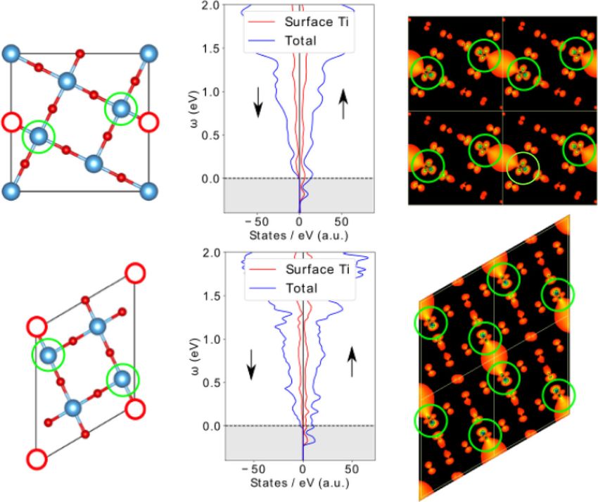
Burke-Ernzerhof (PBE) generalize gradient approximation (GGA) electronic states, similar to the two oxygen vacancy case32. Our
functional30 with the Hubbard U correction in the WIEN2k GGA+U simulations reveal that the highest spin densities are
software package31 to explore the possible magnetism arising found at Ti atoms near the vacancy sites and decreasing for atoms
from the SR-STO. Using the TiO2-terminated STO, we created the further from the vacancies. Those results are consistent with the
surface unit cells shown in Fig. 5a, d with a depth of 5 TiO2 slabs in picture proposed by Lin and Demkov that the magnetism is
the low-temperature tetragonal structure, we simulated the induced by the local orbital mixing due to the oxygen vacancy7.
patterned oxygen vacancies in order to study the vacancy effects Since our system forms a global vacancy pattern, this spin density
on the surface of STO. In our results presented, we considered a distribution forms spin density wave states, which can be seen in
5 × 5 × 1 k-mesh and included spin-orbit coupling along the [001]- Fig. 5c, f. The formation of spin density wave (SDW) states leads us
direction with U = 2 eV. We performed the calculations for both to conclude that the system may be close to the ferromagnetic
paramagnetic and ferromagnetic states and found the ferromag- long-range order, which tends to compete with the super-
netic state to always be the ground state. We also tested different conducting order of the proximity-coupled Nb.
magnetization axes for the spin-orbit coupling ([100] and [010])
and found no discernible difference in the total energies. Magnetic property of SR-STO and interface resistance between
Additionally, we tested U = 1, 2, 3, and 4 eV and found our results superconductor and ferromagnet
were consistent for the entire range of We carried out comprehensive magnetization measurements on
U used. From our calculations, we found a strong non-zero net Al(1 nm)/Nb(d)/SR-STO samples and also a control sample of STO
magnetic moment (12 ðn" n# Þ) on the surface of our SR-STO unit without surface reconstruction for comparison. The upper panel of
cell. To identify the root of this net moment, we first calculated the Fig. 6a shows the magnetization (M), normalized to the surface
projected density of states (PDOS) for the Ti atoms at the surface area of the substrate, as a function of in-plane magnetic field (H //
of our SR-STO unit cell with this initial spin arrangement and ab) for Al(1 nm)/Nb(10 nm)/SR-STO sample at T = 10 K and 300 K,
compared it with the total density of states of our unit cell (Fig. 5b and the M–H curve for the control sample of STO at 10 K is shown
and e). From this, we see the onset of an in-gap peak, as was as blue lines. For ∣μ0H∣ ≥ 0.1 T, the magnetic signal is dominated by
reported previously6,7, which can be mostly attributed to the Ti the diamagnetic moment from the bulk STO, making it difficult to
atoms on the surface as well as a larger population of the spin-up extract the surface magnetic moment contribution in the high
Published in partnership with Nanjing University npj Quantum Materials (2020) 45A.Kr. Singh et al.
6
pffiffiffi pffiffiffi
Fig. 5 The DFT calculations. a–c Refer to the 5 ´ 5 R26.6° structure and d-f refer to the c(4 x 2) structure. a, d show the surface unit cells,
where the open red circles indicate the locations of the oxygen vacancies in the unit cell. All calculations were done with a structure having 5
TiO2 planes thick. b, e show the DOS for the SR-STO structure with U = 2 eV in comparison with the total DOS to show the onset of the spin-
polarized in-gap peaks for the surface Ti atoms. The shaded region in each plot shows the energy range used in calculating the spin densities.
Finally, c, f show the net spin densities for the surface of our SR-STO unit cells, directly correlating with the net magnetic moment due to states
in the energy range shaded in b, e. The color bar represents the values of local magnetic moment calculated from DFT. The regions indicated
by the green circles are referencing the Ti sites neighboring the vacancies, as in the surface unit cells in a, d. By expanding the visible area to
2 × 2 unit cells in the x and y directions, we can see that the presence of periodic, patterned oxygen vacancies leads to the appearance of a
spin density wave.
field regime. We thus focus on the weak field regime, where the field MLH is at least two-fold larger than that in the control sample
diamagnetic background is vanishing small. The apparent of STO without surface reconstruction. For Al(1 nm)/Nb(10 nm)/SR-
hysteresis loop indicates the presence of a ferromagnetic-like STO at T = 10 K, MLH is about 245 and 144 emu cm−2 for H // ab
magnetic signal that persists up to 400 K (see Supplementary and H ⊥ ab, respectively, and MLH values do not vary significantly
Fig. 6). The corresponding differential susceptibility χ = dM/dH is up to 300 K. We also note that similar magnetic behavior was
plotted in the lower panel of Fig. 6b, where the data for Al(1 nm)/ observed for Al(3 nm)/SR-STO sample without Nb layer, suggest-
Nb(10 nm)/SR-STO at T = 300 K and STO control sample at 10 K ing the weak field MLH is intrinsic and deriving from the SR-STO. In
were shifted upward and downward by a magnitude of 0.2 μ emu Fig. 6c, the corresponding Hc values are shown with magnitude
cm−2 G−1, respectively, for clarity. The red open circles and blue less than 50 mT. Those results agree with the possible SDW phase
open squares represent the data points with opposite H sweeping from our DFT calculation and also several earlier reports on the
directions, indicating by the arrows in the figure. The coercive field surface magnetism in oxygen-deficient STO (for a review, please
Hc for Al(1 nm)/Nb(10 nm)/SR-STO, extracted from the local refer to ref. 33). The origin of such an intrinsic weak field MLH
maximum in dM/dH–H curve, equals ≈ 35 mT at T = 10 K, and it remains a debatable issue, where complex spin coupling between
reduces to about 7 mT at T = 300 K. By integrating the dM/dH–H the in-gap spin-polarized states and the itinerant d electrons may
curve, the shaded area shown in the lower panel can be obtained, play an important role. We also notice that, for Al(1 nm)/Nb
giving the weak-field magnetization (MLH) for the ferromagnetic- (15 nm)/SR-STO, the MLH is much reduced at a lower temperature
like contribution. The extracted MLH in four different samples were for H ⊥ ab, which is most likely associated with the presence of
summarized in Fig. 6b with two different field orientations of H// magnetic anisotropy at lower temperatures.
ab (left panel) and H ⊥ ab (right panel). The control sample of STO Based on the existence of such an intrinsic ferromagnetic-like
without surface reconstruction was found to give the lowest MLH magnetism in SR-STO, the physical phases in Al(1 nm)/Nb(d)/SR-
of ≤50 μ emu cm−2 (shaded area in Fig. 6b). It can be attributed to STO system can be illustrated by a cartoon shown in Fig. 7a, where
minute magnetic impurities of a level ≤1 ppm in STO (e.g., 1 ppm the horizontal (blue) arrows represent the magnetization with a
Fe3+ ions give about 200 emu cm−2 with a substrate thickness of declining magnitude as moving away from pffiffiffiffiffiffiffiffithe
ffi Nb/SR-STO
0.05 cm). For other samples using SR-STO as substrate, the weak interface. Within a thickness of about ξh= D=h (D and h are
npj Quantum Materials (2020) 45 Published in partnership with Nanjing UniversityA.Kr. Singh et al.
7
Fig. 6 The magnetization data. The upper panel and lower panel of a show the magnetization and differential susceptibility χ = dM/dH,
respectively, as a function of in-plane magnetic field (H // ab) for Al(1 nm)/Nb(10 nm)/SR-STO sample. A Large weak field hysteresis loop was
observed, which persists up to 300 K, which is in big contrast to the much smaller loop for the control sample of STO without surface
reconstruction (blue lines). The shaded area in the lower panel can be obtained by integrating the dM/dH–H curve, giving the weak field
magnetization (MLH). The dM/dH–H curves for T = 300 K and STO without surface reconstruction at 10K were shifted for clarity. b, c Show the
summaries of the extracted MLH and the corresponding coercive field Hc, respectively, for four different samples at T = 10 K and 300 K with
different field orientations of H // ab (left panel) and H ⊥ ab (right panel). See the main text for more details.
the diffusion coefficient and exchange field, respectively, of the Ri(T) = A=ðew=RNb þ 1Þ C, where A, w and C are some constants,
ferromagnet34), there is a proximity-induced superconducting and RNb is the sheet resistance of the Nb thin film from the control
regime on the SR-STO side, which forms a superconductor/ sample using SiO2/Si as a substrate. As an example in Fig. 7c, the
ferromagnet (SC/FM) interface shown as green dashed line in the simulated effective sheet resistance (Reff) of the resistor network
cartoon. Considering a one dimensional spin diffusion model (blue line), using Ri(T) and the the corresponding RNb and RSR−STO
across a SC/FM interface, the boundary conditions at the interface from control samples, can reasonably reproduce the resistance
require both μ↑ (x = 0) = −μ↓(x = 0) and j↑(x = 0) = j↓(x = 0) due to peak feature found in the experimental Rs data (open circles) of Al
constraints from Andreev reflection effect and zero net spin (1 nm)/Nb(10 nm)/SR-STO sample. Nevertheless, considering the
current on SC side35 (Fig. 7b), where μ↑(↓) is the chemical potential macroscopic junction area (~1 mm2) in our samples, the simulated
for spin up (down) electrons, and spin current density j↑(↓) = SC/FM interface resistance Ri of about 2.2 mΩ turns out to be only
−(σ↑(↓)/e)∂μ↑(↓)/∂x. The SC/FM interface resistance can be possible with a fully spin-polarized state in the FM (1 − p ≤ 10−6) if
expressed as Ri = Δμ/ej = ½p2 =ð1 p2 ÞðρF λFSF Þ29,35, where p = (σ↑ − we take ρF = 0.01 Ω × 10−5 cm and λFSF = 10−5 cm. It is not clear
σ↓)/(σ↑ + σ↓) and ρF (λFSF ) are the spin-polarization and resistivity whether a field-enhanced exchange coupling for the in-gap states
(spin-diffusion length), respectively, of the FM. For T < Tc, the SC/ can lead to such a fully spin-polarized state. While more complex
FM interface is located within the SR-STO, and it disappears as the model than resistor network may be required, further investiga-
temperature goes above Tc. A simplified resistor network model tions are also needed to reveal the spin-polarization and other
for the Al(1 nm)/Nb(d)/SR-STO system can then be constructed spin-related parameters near the surface of a SR-STO under
and shown in the inset cartoon of Fig. 7c. As T increases across the magnetic field.
superconducting transition, Ri transforms from the resistance of a To justify the resistor network model, we construct a SC/FM/SC
SC/FM interface to that of a metal/FM interface, and the interface layered tight-binding model shown in the upper panel in Fig. 7d
resistance changes across Tc can be expressed as to investigate the conductance across the SC/FM interface. To
fp2 minimize the finite size effect, a periodic boundary condition
ΔRi ¼ Ri ðT < T c Þ Ri ðT > T c Þ ¼ ρ λF ; (1) between SC layers on both sides is introduced. The ferromagnet-
ð1 p2 Þð1 p2 þ f Þ F SF
ism is introduced by the spin-dependent chemical potential μσ =
where f = ρF λFSF =ρN λNSF and ρN (λNSF ) is the resistivity (spin diffusion EF − σM, where M is the ferromagnetic order parameter. In SC
length) of the Nb in normal state. We remark that ΔRi is always layers, the superconducting gap Δ is introduced via the standard
positive and diverges as p approaches one that corresponds to a BCS mean-field pairing Hamiltonian. The interface is modeled by
fully spin-polarized state in the FM. We then model a step-like the barrier potential Vb which is similar to the Z parameter used
function for the temperature dependent interface resistance of in the Blonder-Tinkham-Klapwijk (BTK) formalism36. The
Published in partnership with Nanjing University npj Quantum Materials (2020) 45A.Kr. Singh et al.
8
Fig. 7 The resistor network model with SC/FM interface resistance. a An illustration of the proximity coupled Al(1 nm)/Nb(d)/SR-STO system.
The blue horizontal arrows represent the magnetization in SR-STO, and the green dashed line is an SC/FM interface between the proximity-
induced SC region and the rest of SR-STO. b The spin-up (spin-down) chemical potential μ↑(↓) across a SC/FM interface, and x is the distance to
the interface. A boundary condition of μ↑(x = 0) = −μ↓(x = 0) was introduced to respect the constraint due to the Andreev reflection effect.
The interface resistance Ri = Δμ/ej can then be determined using a one dimensional spin diffusion model. A simplified resistor network model
is shown in the inset cartoon of (c). The resistance peak feature for the Al(1 nm)/Nb(10 nm)/SR-STO with an in-plane field of μ0H = 5 T is well
reproduced by the simulated effective resistance Reff of the proposed resistor network (blue line). The dashed black and red lines are the
corresponding RNb and Ri for the simulated Reff. The geometry of the SC/FM/SC layered model is shown in the upper panel of (d). There are N1
layers for SC on both sides and N2 layers for FM. The lower panel of d shows the normalized zero-energy conductance GN(Δ, E = 0) in the
transparent limit.
tight-binding Hamiltonian can be written as Green’s function. We compute the conductance from i ¼ z 0 1
(the last layer of SC on the left) to j = z″ (the last layer of FM), as
^¼H
H ^ FM þ H ^L þ H^R ;
SC SC shown in the upper panel of Fig. 7d to capture the Andreev
PP z00 reflection near the SC/FM interface. In all the calculations
^ ¼
H
FM
ϵ ðkÞ μσ þ ðδz;z0 þ δz;z00 ÞV b cyk;z;σ ck;z;σ
FM
kσ z¼z 0
presented here, we put N1 = N2 = 200 and tSC/t = 4.
We focus on the conductance at zero energy, which corresponds
þ ðtcyk;z;σ ck;zþ1;σ þ h:c:Þ;
to the resistance used in the resistor network model (Ri ~ 1/G(0)). In
N1 P
PP
^L ¼
H ϵSC ðkÞ E F cyk;z;σ ck;z;σ the lower panel of Fig. 7d, we plot the zero-energy conductance
σ
SC
k z¼1 normalized to the normal state one, defined as GN(Δ, E = 0) ≡ Gij(Δ,
þðtSC cyk;z;σ ck;zþ1;σ þ h:c:Þ þ ðΔcyk;z;" cyk;z;# þ h:c:Þ; E = 0)/Gij(Δ = 0, E = 0), as a function of Δ with (Vb, M) fixed. Since our
sample is likely to be in the transparent limit, we set Vb = 0 in the
1 þN 2 P
P 2NP
^R ¼ cyk;z;σ ck;z;σ þ ðt SC cyk;z;σ ck;zþ1;σ þ h:c:Þ calculation. It is confirmed that the normalized zero-energy
σ ϵ ðkÞ E F
SC
H SC
k z¼z00 þ1 conductance across the SC/FM interface for the FM layers with large
þ ðΔcyk;z;" cyk;z;# þ h:c:Þ; M always decreases with Δ and saturates to a certain value for large
Δ, due to the suppression of the Andreev reflection by the spin
(2)
polarization. On the contrary, for small M the normalized zero-energy
where there are N1 layers for SC at both sides and N2 layers for FM, conductance increases with Δ, because the Andreev reflection
z 0 ¼ N1 þ 1 and z″ = N1 + N2 are the layer indices for the remains robust forpsmall spin polarization. Since from the BCS theory
ffiffiffiffiffiffiffiffiffiffiffiffiffiffiffiffiffiffi
interfacial layers, k is the in-plane momentum, ΔðTÞ / ΔðT ¼ 0Þ 1 T=T c , our calculation suggests that the zero-
ϵFM ¼ 2tðcos k x þ cos k y Þ, and ϵSC ¼ 2tSC ðcos k x þ cos k y Þ. With energy interfacial conductance for the FM layers with large spin
this Hamiltonian, we can use the Landauer formula to compute polarization will monotonically decrease with the temperature below
the conductance between layers i and j: Tc, which justifies the step-like temperature profile of the interfacial
2 P 2 resistance Ri proposed in the resistor network model.
Gij ðEÞ ¼ 2eh k T ij ðEÞ ; T ij ðEÞ ¼ jGij ðE; kÞj ;
k k R
We further fabricated superconductor/SR-STO heterostructure
(3)
GRij ðE; kÞ ¼ ðE þ iηÞ^I H ^ k 1 ; using different superconducting layers of lanthanum (La) and
ij
aluminum (see Supplementary Fig. 7). Similar resistance peak
where T kij ðEÞ is the transmission probability from layer i to j with in- phenomenon was observed in La(20 nm)/SR-STO sample, and the
plane momentum k, and GRij ðE; kÞ is the corresponding retarded magnitude of resistance peak (Δr) increases with increasing
npj Quantum Materials (2020) 45 Published in partnership with Nanjing UniversityA.Kr. Singh et al.
9
in-plane field strength, which is in accord with the field-induced Received: 29 November 2019; Accepted: 2 June 2020;
resistance peak in Al(1 nm)/Nb(d)/SR-STO samples. However, we
do notice that Δr is nearly 5-fold smaller as compared to Nb
(10 nm)/SR-STO sample at similar field strength. Such a notable
variation in Δr at similar field strength may be attributed to the
difficulty in the experimental control over the interface quality and REFERENCES
1. Tarascon, J. M., Greene, L. H., Mckinnon, W. R., Hull, G. W. & Geballe, T. H.
thus the barrier potential (Vb) that can affect the interface
Superconductivity at 40 K in the oxygen-defect perovskites La2−xSrxCuO4−y. Sci-
resistance, according to the DFT calculations (Fig. 7d). ence 235, 1373–1376 (1987).
We studied the superconducting property in proximity coupled 2. Cava, R. J. et al. Bulk superconductivity at 91 K in single-phase oxygen-deficient
Al(1 nm)/Nb(d)/SR-STO system. With proper
pffiffiffi pffiffipreparations,
ffi SR-STO perovskite Ba2YCu3O9−δ. Phys. Rev. Lett. 58, 1676–1679 (1987).
substrates with surface structures of 5 ´ 5 R26:6o and c(4 × 2) 3. Liang, R., Bonn, D. A. & Hardy, W. N. Evaluation of CuO2 plane hole doping in
can be well reproduced, and the corresponding electronic YBa2Cu3O6+x single crystals. Phys. Rev. B 73, 180505 (2006).
property not only exhibits strong electron–phonon coupling 4. Spinelli, A., Torija, M. A., Liu, C., Jan, C. & Leighton, C. Electronic transport in doped
SrTiO3 : conduction mechanisms and potential applications. Phys. Rev. B 81,
effect but also shows intriguing spin-polarized in-gap states based 155110 (2010).
on the DFT calculations. While those spin-polarized states do not 5. Lin, X., Zhu, Z., Fauque, B. & Behnia, K. Fermi surface of the most dilute super-
give a long-range magnetic order in weak fields, a larger field can, conductor. Phys. Rev. X 3, 021002 (2013).
in principle, promote the long-range magnetic order in SR-STO, 6. Lin, C. & Demkov, A. A. Electron correlation in oxygen vacancy in SrTiO3. Phys. Rev.
making it an intriguing example of proximity coupled super- Lett. 111, 217601 (2013).
conductor/ferromagnet bilayer. We uncovered a notable region in 7. Lin, C. & Demkov, A. A. Consequences of oxygen-vacancy correlations at the
SrTiO3 interface. Phys. Rev. Lett. 113, 157602 (2014).
the H–T phase diagram, showing unusual resistance peak 8. Altmeyer, M. et al. Magnetism, spin texture, and in-gap states: atomic speciali-
phenomenon. Such a field-induced resistance peak can be zation at the surface of oxygen-deficient SrTiO3. Phys. Rev. Lett. 116, 157203
attributed to the proximity coupling of the superconducting Nb (2016).
to the spin-polarized in-gap states with possible field-assisted 9. Meevasana, W. et al. Creation and control of a two-dimensional electron liquid at
long-range magnetic order. By using a simplified resistor network the bare SrTiO3 surface. Nat. Mater. 10, 114–118 (2011).
model with a step-like interface resistance (Ri(T)), the resistance 10. Tanaka, H., Matsumoto, T., Kawai, T. & Kawai, S. Surface structure and electronic
property of reduced SrTiO3 (100) surface observed by scanning tunneling
peak behavior can be explained, and the extracted Ri value for SC/ microscopy/spectroscopy. Jpn. J. Appl. Phys. 32, 1405–1409 (1993).
FM interface is on the order of a few mΩ that may infer a fully 11. Wang, Q. Y. et al. Interface-induced high-temperature superconductivity in single
spin-polarized FM state in the SR-STO under magnetic field. Similar unit-cell FeSe films on SrTiO3. Chin. Phys. Lett. 29, 037402 (2012).
resistance peak phenomenon was also observed using La as the 12. Lee, J. J. et al. Interfacial mode coupling as the origin of the enhancement of Tc in
superconducting layer, justifying the generic feature of the peak FeSe films on SrTiO3. Nature 515, 245–248 (2014).
resistance effect in a superconductor/SR-STO heterostructure. Our 13. Ding, H. et al. High-temperature superconductivity in single-unit-cell FeSe films
on Anatase TiO2 (001). Phys. Rev. Lett. 117, 067001 (2016).
work provides an intriguing way of revealing the unusual
14. He, S. et al. Phase diagram and electronic indication of high-temperature super-
electronic states in the SR-STO due to oxygen vacancies by conductivity at 65 K in single-layer FeSe films. Nat. Mater. 12, 605–610 (2013).
proximity-coupling to a superconductor. 15. Gonzalez, M. S. M. et al. In situ reduction of (100) SrTiO3. Solid State Sci. 2, 519–524
(2000).
16. Chen, C., Avila, J., Frantzeskakis, E., Levy, A. & Asensio, M. C. Observation of a two-
METHODS dimensional liquid of Frohlich polarons at the bare SrTiO3 surface. Nat. commun.
A series of TiO2 terminated STO substrates were slowly heated up and 6, 8585 (2015).
annealed in an UHV LEED chamber at temperatures ranging from 800 °C to 17. Dagdeviren, O. E. et al. Surface phase, morphology, and charge distribution
900 °C followed by LEED measurements to characterize the surface transitions on vacuum and ambient annealed SrTiO3 (100). Phys., Rev. B 93,
structures of the STO substrates. In order to ensure the best surface 195303 (2016).
18. LEEDpat, Version 4.2, utility by K.E. Hermann (FHI) and M.A. Van Hove (HKBU),
quality of STO, the SR-STO substrates were annealed in an UHV chamber
Berlin/Hong Kong. http://www.fhi-berlin.mpg.de/KHsoftware/LEEDpat/index.html
and then transferred directly under UHV environment to another UHV
(2014).
electron beam evaporator chamber for niobium film deposition at ambient
19. Yoshii, K., Yamamoto, H., Saiki, K. & Koma, A. Superconductivity and electrical
temperature, where the base pressure during the film deposition was kept properties in single-crystalline ultrathin Nb films grown by molecular-beam
as low as 5 × 10⁻¹¹ torr. The film thickness was monitored using a quartz epitaxy. Phys. Rev. B 52, 13570–13575 (1995).
crystal microbalance, where the deposition rate was precalibrated by X-ray 20. Tinkham, M. Introduction to Superconductivity. (Dover Publications, New York,
low-angle reflectivity measurements. At last, a thin aluminum film of 1996).
thickness about 1 nm was subsequently deposited as a protection layer. 21. Suzuki, M. Resistance peak at the resistive transition in high-Tc superconductors.
The surface morphology of resulting Al(1 nm)/Nb(d)/SR-STO samples were Phys. Rev. B 50, 6360–6365 (1994).
probed using an atomic force microscope. The magnetotransport 22. Wan, Y. M., Hebboul, S. E., Harris, D. C. & Garland, J. C. Interlayer Josephson
measurements were carried out using a superconducting magnet system coupling of thermally excited vortices in Bi2Sr2CaCu208−y. Phys. Rev. Lett. 71,
with a variable temperature insert. For comparison, a series of control 157–160 (1993).
samples were fabricated with the same conditions of films deposited either 23. He, Z. et al. Observation of resistivity anisotropy on oriented YBa2Cu3O7 films.
on TiO2-terminated STO without surface reconstruction or on SiO2/Si Solid State Commun. 76, 671–674 (1990).
substrates instead. 24. Buzea, C. & Yamashita, T. Structure anisotropy of high temperature super-
conductors: resistance peak effect. J. Optoelectron. Adv. Mater. 2, 704–712 (2000).
25. Santhanam, P., Chi, C. C., Wind, S. J., Brady, M. J. & Bucchignano, J. J. Resistance
DATA AVAILABILITY anomaly near the superconducting transition temperature in short aluminum
wires. Phys. Rev. Lett. 66, 2254–2257 (1991).
All the supporting data are included in the main text and also in Supplementary
26. Moshchalkov, V. V., Gielen, L., Neuttiens, G., Van Haesendonck, C. & Bruynseraede,
information. The raw data and other related data for this paper can be requested
Y. Intrinsic resistance fluctuations in mesoscopic superconducting wires. Phys.
from W.L.L. (wlee@phys.sinica.edu.tw).
Rev. B 49, 15412–15415 (1994).
27. Sambandamurthy, G., Engel, L. W., Johansson, A., Peled, E. & Shahar, D. Experi-
mental evidence for a collective insulating state in two-dimensional super-
CODE AVAILABILITY conductors. Phys. Rev. Lett. 94, 017003 (2005).
The input files for DFT calculations using WIEN2k are available upon request. The 28. Zhang, G., Zeleznik, M., Vanacken, J., May, P. W. & Moshchalkov, V. V. Metal-
computer code for the calculation of Landauer conductance is written in FORTRAN90 bosonic insulator-superconductor transition in boron-doped granular diamond.
and is also available upon request. Phys. Rev. Lett. 110, 077001 (2013).
Published in partnership with Nanjing University npj Quantum Materials (2020) 45A.Kr. Singh et al.
10
29. Wang, J. et al. Interplay between superconductivity and ferromagnetism in COMPETING INTERESTS
crystalline nanowires. Nat. Phys. 6, 389–394 (2010). The authors declare no competing interests.
30. Perdew, J. P., Burke, K. & Ernzerhof, M. Generalized gradient approximation made
simple. Phys. Rev. Lett. 77, 3865–3868 (1996).
31. Blaha, P. et al. WIEN2k, an augmented plane wave + local orbitals program for cal- ADDITIONAL INFORMATION
culating crystal properties (Karlheinz Schwarz, Techn. Universität Wien, Austria, 2018).
Supplementary information is available for this paper at https://doi.org/10.1038/
32. Lechermann, F., Jeschke, H. O., Kim, A. J., Backes, S. & Valentin, R. Electron
s41535-020-0242-4.
dichotomy on the SrTiO3 defect surface augmented by many-body effects. Phys.
Rev. B 93, 121103 (2016).
Correspondence and requests for materials should be addressed to W.-C.L. or W.-L.L.
33. Coey, J. M. D., Venkatesan, M. & Stamenov, P. Surface magnetism of strontium
titanate. Matter 28, 485001 (2016).
Reprints and permission information is available at http://www.nature.com/
34. Bergeret, F. S., Volkov, A. F. & Efetov, K. B. Long-range proximity effects in
reprints
superconductor-ferromagnet structures. Phys. Rev. Lett. 86, 4096–4099 (2001).
35. Jedema, F. J., van Wees, B. J., Hoving, B. H., Filip, A. T. & Klapwijk, T. M. Spin-
Publisher’s note Springer Nature remains neutral with regard to jurisdictional claims
accumulation-induced resistance in mesoscopic ferromagnet-superconductor
in published maps and institutional affiliations.
junctions. Phys. Rev. B 60, 16549–16552 (1999).
36. Blonder, G. E., Tinkham, M. & Klapwijk, T. M. Transition from metallic to tunneling
regimes in superconducting microconstrictions: excess current, charge imbal-
ance, and supercurrent conversion. Phys. Rev. B 25, 4515–4532 (1982).
ACKNOWLEDGEMENTS Open Access This article is licensed under a Creative Commons
W.L.L. acknowledges the funding supports from Academia Sinica (Thematic Research Attribution 4.0 International License, which permits use, sharing,
Program) and Ministry of Science and Technology of Taiwan (MOST Grant No. MOST adaptation, distribution and reproduction in any medium or format, as long as you give
108-2628-M-001-007-MY3). M.D.R. and W.-C.L. were supported by the National appropriate credit to the original author(s) and the source, provide a link to the Creative
Science Foundation under Grant No. NSF-IIS-2026702. We also thank C. Lin, W. Wu, A. Commons license, and indicate if changes were made. The images or other third party
Bensaoula, and Y. Matsuda for fruitful discussions. material in this article are included in the article’s Creative Commons license, unless
indicated otherwise in a credit line to the material. If material is not included in the
article’s Creative Commons license and your intended use is not permitted by statutory
AUTHOR CONTRIBUTIONS regulation or exceeds the permitted use, you will need to obtain permission directly
from the copyright holder. To view a copy of this license, visit http://creativecommons.
A.K.S. and U.K. grew the epitaxial films. T.C.W., B.D., S.K., and W.L.L. carried out the low
org/licenses/by/4.0/.
temperature magneto-transport measurements and data analysis. W.H.P. and A.K.S.
performed LEED measurements and analysis. M.D.R. and W.C.L. constructed
theoretical model and calculation. A.K.S., W.C.L., and W.L.L. designed the experiment
© The Author(s) 2020
and wrote the paper.
npj Quantum Materials (2020) 45 Published in partnership with Nanjing UniversityYou can also read