Humidity sensor based on Gallium Nitride for real time monitoring applications
←
→
Page content transcription
If your browser does not render page correctly, please read the page content below
www.nature.com/scientificreports
OPEN Humidity sensor based on Gallium
Nitride for real time monitoring
applications
Chaudhry Muhammad Furqan1,2,6, Muhammad Umair Khan2,3,6, Muhammad Awais4,6,
Fulong Jiang5, Jinho Bae3*, Arshad Hassan4* & Hoi‑Sing Kwok1,2*
Gallium Nitride (GaN) remarkably shows high electron mobility, wide energy band gap,
biocompatibility, and chemical stability. Wurtzite structure makes topmost Gallium atoms
electropositive, hence high ligand binding ability especially to anions, making it usable as humidity
sensor due to water self-ionization phenomenon. In this work, thin-film GaN based humidity sensor is
fabricated through pulse modulated DC magnetron sputtering. Interdigitated electrodes (IDEs) with
100 μm width and spacing were inkjet printed on top of GaN sensing layer to further enhance sensor
sensitivity. Impedance, capacitance, and current response were recorded for humidity and bio-sensing
applications. The sensor shows approximate linear impedance response between 0 and 100% humidity
range, the sensitivity of 8.53 nF/RH% and 79 kΩ/RH% for capacitance and impedance, and fast
response (Tres) and recovery (Trec) time of 3.5 s and 9 s, respectively. The sensor shows little hysteresis
of < 3.53% with stable and wide variations for accurate measurements. Especially, it demonstrates
temperature invariance for thermal stability. Experimental results demonstrate fabricated sensor
effectively evaluates plant transpiration cycle through water level monitoring by direct attachment
onto leaves without causing any damage as well as freshness level of meat loaf. These properties of
the proposed sensor make it a suitable candidate for future electronics providing a low-cost platform
for real time monitoring applications.
Atmosphere contains water molecules in gaseous state and creates humid conditions in the environment. Con-
centration of water molecules is generally measured as a relative parameter called relative humidity (RH). Tem-
perature and humidity are interdependent and have complex and varied effects on objects1. Objects/substances
not only get affected by the concentration of water molecules but also by the rate of change in ambience. Humidity
affects (biological growth, mechanical strength, chemical degradation, building damage, metal corrosion, etc.) if
not maintained in a suitable range, making its accurate measurement n ecessary2. Plants play a vital role in main-
tenance of hydrologic response and water stress through transpiration, taking up CO2 and releasing H2O cooling
off the surface3. Thus, humidity and temperature show interdependence making accurate measurements difficult.
Thus, accurate measurement of RH is perplexed and difficult as compared to other environmental factors.
In recent years, researchers investigated semiconducting metal o xides4,5, graphene6, carbon nano-tubes
(CNTs) , carbon quantum dots (CQDs) , transition metal dichalchogenides (TMDCs)11,12, and composites12–14
7–9 10
for humidity sensing applications because of ease of fabrication and low cost. However, most of these materi-
als have intrinsic drawbacks, like metal oxides have a non-linear response, graphene has almost zero band gap
energy, and TMDCs have limited detection range. Semiconductors are synthesized from group II to VI, in
which silicon Si is the most widely used m aterial15. Porous silicon (PSi) gets corroded and is instable leading to
restrictions in humidity sensing applications4. Moisture sensing properties of gallium nitride (GaN) have been
exploited in recent years16,17 and it can be employed for humidity sensing applications.
1
State Key Laboratory on Advanced Displays and Optoelectronics Technologies, The Hong Kong University
of Science and Technology, Clear Water Bay, Kowloon, Hong Kong. 2Department of Electronic and Computer
Engineering, The Hong Kong University of Science and Technology, Clear Water Bay, Kowloon, Hong
Kong. 3Department of Ocean System Engineering, JEJU National University, 102 Jejudaehakro, Jeju 63243,
Republic of Korea. 4National University of Computer and Emerging Sciences (NUCES-FAST), Islamabad 44000,
Pakistan. 5Department of Electrical and Electronic Engineering, Southern University of Science and Technology,
Shenzhen 518000, China. 6These authors contributed equally: Chaudhry Muhammad Furqan, Muhammad Umair
Khan and Muhammad Awais. *email: baejh@jejunu.ac.kr; arshad.hassan@nu.edu.pk; eekwok@ust.hk
Scientific Reports | (2021) 11:11088 | https://doi.org/10.1038/s41598-021-89956-0 1
Vol.:(0123456789)
www.nature.com/scientificreports/
The crystal structure of GaN is similar to the Wurtzite (ZnS) structure18. The outermost layer of Gallium in a
Wurtzite crystal has three bonds with underlying Nitrogen atoms, while the fourth place is readily available for
reaction with ligands, especially a nions19. Hydrolysis of GaN is difficult and does not react with hydrochloric
or nitric acids, but dissolves slowly in hot concentrated sulfuric a cid18. Melting point of GaN is > 2500 °C, these
properties make it a highly stable material for humidity sensing applications. The calculated density of GaN is
6200 kg m −320. Due to high electron mobility of GaN High Electron Mobility Transistors (HEMTs) are being
fabricated by utilizing G aN4,21. Devices of GaN can safely operate at high terminal voltages up to 42 V 21 due to
high impedance and are preferable for low power consumption, or in other words low power dissipation4. It
shows a wide bandgap energy of 3.4 eV at 300 K reliable for high-voltage and temperature operations. A fast
response and recovery time for adsorption of H 2O molecules on GaN was calculated ≈ 6.8 × 10⁻³ s22. In addi-
tion, GaN shows bio-compatible properties, an extensive network of neurons was found after seeding on GaN
surface23, and human embryonic kidney cells were grown on AlGaN/GaN heterostructures24. Thus, GaN surface
facilitates neuronal cell attachment and tissue growth without specialized surface treatment. Therefore, GaN can
be engaged as a highly sensitive and real time humidity sensor at bio-interfaces.
Gallium Nitride is difficult to grow utilizing conventional m ethods25. Temperatures > 800 °C are required
for GaN epitaxial growth26. Until 926.85 °C GaN is stable and can be stabilized in increased pressures27. Sput-
tering process deposits atoms, molecules or fragments from a target bombarded with high energy particles or
ions. Magnetron sputtering process is widely used for fabrication of high quality thin fi lms28. Pulsed magnetron
sputtering (PMS) enables deposition and growth of dielectric materials. Pulsed sputtering process reduces the
risk of DC arc events and stabilizes thin film growth with reduced defects29–31. Advantages of PMS include high
deposition rate, high adhesion to substrate, uniformity of deposition and high purity31. Thus, enhanced structural,
optical and electrical properties can be achieved through PMS coating technique29.
In this paper, we present a highly stable, reliable and fast humidity sensor capable of all range humidity detec-
tion between 0 and 100% RH based on pulsed modulated DC magnetron sputtering of GaN on glass substrate.
Interdigitated electrodes (IDEs) are printed on top of sensing layer to enhance the electrical sensitivity of the
proposed sensor. The proposed sensor shows linear impedance response towards all range humidity, capacitive
and impedance sensitivity of ~ 8.53 nF/RH% and ~ 79 kΩ/RH%, respectively. A fast response and recovery
time of ~ 3.5 s and ~ 9 s, respectively, was recorded with little hysteresis of < 3.53%. It also has low temperature
dependence, thus, sensor capabilities can be incorporated with real time bio-sensing for smart agriculture and
food freshness applications. Smart agriculture not only requires conservation of water but also monitoring of soil
acidity and resources for increased crop production from plants. Transpiration monitoring can help accumulate
the required data through sensing network. Food quality and wastage are another concern for modern day-to-
day life affecting human health especially meat products, thus, evaluation of meat freshness can be conducted
via sensor attachment during packaging process. We demonstrate efficacy and suitability of proposed sensor for
these applications with a low-cost sensor.
Experimental section
Sensor fabrication. Glass slide was used as substrate material after cleaning process, 20 nm buffer layer
of ZnO was prepared by sputtering to improve crystal quality of GaN thin film. High purity liquid Ga target
(99.99999%) with a mixture of sputtered gasses (N2 and Ar) at 41:9 sccm flow rate were used for GaN thin film
deposition. The base pressure of vacuum chamber was pumped down to 1 × 10⁻⁶ Torr to avoid any moisture
influence. The substrate was preheated to 450 °C and chamber pressure was maintained at 7.5 mT with a pulse
width of 70 μs and an average power of 70 W, respectively. Resultantly, a 300 nm GaN thin film was deposited by
pulsed DC magnetron sputtering process.
The IDEs were designed using EAGLE software platform in dxf format then converted to bmp format using
ACE 3000 and exported to Dimatix Drop manager software. The Dimatix manager converts the bmp file into ptn
format loadable to Fujifilm Dimatix DMP-3000 inkjet printer. Silver nanoparticles (Ag NPs) ink was loaded in 16
nozzle 10 pL cartridge with diameter of 9 μm. A 30 V biasing voltage was applied on nozzles with drop spacing of
20 μm with temperature regulation of 30 °C of the movable platform. Silver electrodes were deposited on the top
of GaN thin film via inkjet printing process having 100 μm width and 100 μm spacing. Electrodes were cured at
temperature of 120 °C for 1 h. Figure 1 shows schematic illustration of printing process of the humidity sensor.
Characterizations. TESCAN MIRA 3 scanning transmission electron microscope (STEM) and energy
dispersive X-Ray spectroscope (EDS) were used to examine elemental composition and surface morphology
of the sensing layer as well as IDEs. A STEM image of sensing layer GaN with electron beam accelerated at
15 kV and 2.5 μm sizing is shown in Fig. 2a confirming uniform fabrication of active layer through sputtering
technique. The EDS mapped image confirms presence of Nitrogen K series and Gallium L series in Fig. 2b and
c, respectively. After deposition of Ag IDEs on top of active GaN layer, SEM image is presented in Fig. 2d at
magnification of 100 μm validating uniform fabrication. Rough edges of IDEs are observed after curing at 120
°C. The EDS mapped images in Fig. 2e and f endorse presence of Silver K series and Carbon L series, respectively.
A non-contact surface profiler NV-2000 was used to analyze the surface roughness and height of GaN. The 3D
nano-profile arithmetic mean (Ra), RMS (Rq), and height profiles (Rz)32,33 of GaN were found to be 76.85 nm,
90.01 nm and 380.86 nm as shown in Fig. 2g. Similarly, for surface roughness and height of IDE layers, the Ra, Rq,
and Rz of Ag IDEs were found to be 3.06 μm, 3.35 μm and 11.79 μm, respectively, shown in Fig. 2h. These results
ensure correct fabrication of GaN layer through magnetron sputtering and IDEs via inkjet printing techniques.
XPS Spectrum was measured by PHI 5600 (Physical Electronics) with source of Al X-ray monochromator.
XPS spectrum of GaN with having peaks of Carbon, Nitrogen and Gallium presented in Fig. 3a. C 1s peak was
adjusted at 285.0 eV for the calibration of absolute binding energy. De-convoluted spectra with core levels of Ga
Scientific Reports | (2021) 11:11088 | https://doi.org/10.1038/s41598-021-89956-0 2
Vol:.(1234567890)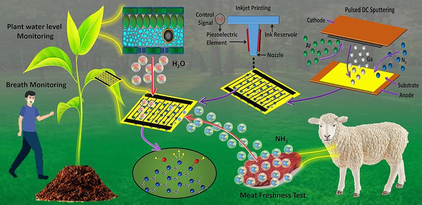
www.nature.com/scientificreports/
Figure 1. Schematic illustration of fabrication process of humidity sensor.
3d in Fig. 3b, N 1s Fig. 3c and O 1s Fig. 3d from the surface of the sample. High resolution N-1s reveals three
sub peaks at 397.20 eV confirm the bonding of N–Ga and other two peaks at 394.51 and 396.2 eV correspond
towards Auger Ga. The dominant peak at 20.10 eV and Lorentzian fitted peak at 19.46 in high resolution are
attributed towards the Ga–N and Ga–O bonds, respectively34,35. X-ray diffraction pattern (XRD) was recorded
by Empyrean (PANalytical) diffractometer using CuKα radiation of wavelength λ = 1.5406 nm in the scan range
2θ = 20°–70° as shown in Fig. 3e. The diffraction peaks are labelled as (002) and (103) at angles of 34.4° and
62.4°. XRD analysis was revealed the Polycrystalline structure of GaN, it has wurtzite structure with sharp and
high peak of (002) c-axis orientation with FWHM of (0.4821). The average crystallite size was calculated by
Debye–scherrer approximation, which is found to be 30 n m36. Raman Spectrum was measured by HORIBA
LabRAM HR confocal spectrometer, equipped with 800 nm length monochromator, He–Cd laser was shined on
the surface of the sample with the excitation wavelength of 325 nm. RT Raman Spectra of GaN was taken which
shows the two corresponding signature peaks of E2 (high) and A1 (LO) modes can be seen in Fig. 3f, predicts the
figure prints of hexagonal wurtzite structure of GaN. Epitaxial GaN layer grown on sapphire shows the actual
raman peaks at 570.4 c m−1 and 736.2 c m−1 for E2 (high) and A 1 (LO) modes, in correspondence of our raman
peaks located at 566.3 cm−1 and 731.5 cm−1 for E
2 (high) and A1 (LO) modes, respectively. These relative shift of
peaks are due to the in plane compressive stress between GaN thin film on ZnO buffer layer originated because
of slightly un matched lattice c onstant37,38.
Humidity test setup. A customized testing chamber was made for observations in change of impedance
and capacitance of the sensor with increase in RH. The humidity was increased slowly from 0 to 100% RH
through atomizer via ultrasonic humidifier, for dehumidification from 100 to 10% RH compressed air was used,
and dry N2 gas was used between 10 and 0% RH both controlled via electronic flow control valves. A high
accuracy commercially available humidity sensor HTU21D is used as reference with response < 5 s, resolution
of 0.04% RH and accuracy of ± 2% RH. Electronic valves are regulated through a control board and an Arduino
UNO is connected for data sampling and logging connected to computer via Universal Serial Bus (USB) cable.
Block diagram is shown in Fig. 4a.
Results and discussion
Impedance and capacitance response. During experimentation impedance is observed by slowly
variating ambient humidity conditions with intervals after variations for stabilization of response. The RH is
increased from 0 to 100% with a stepping of 10%. Impedance magnitude of the sensor follows the Eq. (1):
1
Z =R+ (1)
j2πfC
√
Here, C is the terminal capacitance of the sensor, f is the observing frequency, j = −1 , and R is the sheet
resistance of the sensing layer. Impedance values are presented as absolute values |Z|. Figure 4b shows the
impedance response for both simulation as well as experiment at 1 kHz frequency. The impedance at 1 kHz
starts at 9 MΩ at 0% RH and starts to decrease as the RH increases, till 100% RH the impedance drops down
to 0.982 MΩ. This drop in impedance is due to cumulative sheet resistance and capacitive impedance drop. At
low frequencies the capacitive impedance drops down to a certain minimum with increase in frequency, then
inductive impedance overwhelms the capacitive behaviour. From the results it can be observed that both results
match each other. A slight difference observed is attributed to surface roughness of GaN and IDEs. At 10 kHz
the impedance response is discussed in supplementary Fig. S1(a).
Scientific Reports | (2021) 11:11088 | https://doi.org/10.1038/s41598-021-89956-0 3
Vol.:(0123456789)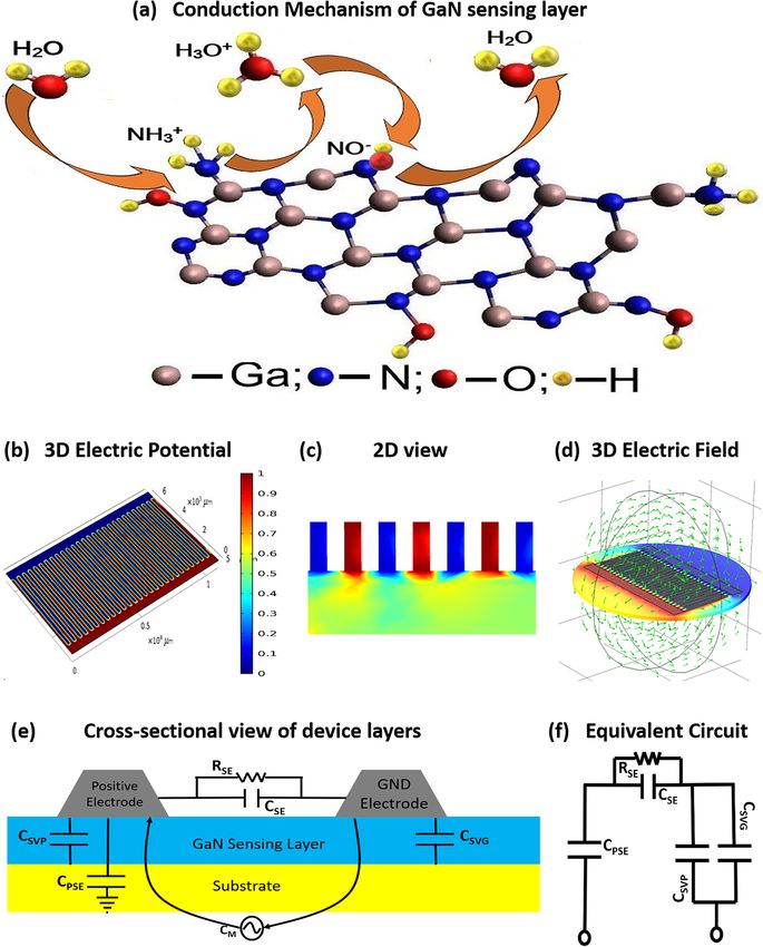
www.nature.com/scientificreports/
Figure 2. (a) STEM GaN layer, (b) nitrogen K series, (c) Ga L series, (d) STEM IDEs (e) silver L series, (f)
carbon K series, nano-profile (g) GaN, and (h) IDEs.
Similarly, the capacitance of the sensing layer also shows humidity dependence. As the ambient humidity
conditions start to increase the relative permittivity of the GaN layer increases due to absorption and adsorption
of OH- and H+ ions. The frequency dependence of capacitance is given in Eq. (2)39,40:
Ceff = ε∗ Co = εr − j γ 2πf εo Co (2)
Here, f is the frequency, Ceff is the effective capacitance, Co is the expected capacitance, ε∗ is the complex
dielectric, εr is the relative dielectric constant compared to εo the free space dielectric, and γ is the conductance.
Figure 4b shows capacitance response for both simulation and experiment as a function of RH at 1 kHz. At 0%
RH the capacitance observed is 15.2 nF. Capacitance starts to increase as RH increases and reaches a maximum
of 882.8 nF at 100% RH. Both results match each other, however, a slight difference observed is attributed to
uneven spacing between IDEs visible in Fig. 2e. The experimental capacitance response at 10 kHz frequency is
discussed in supplementary Fig. S1(b).
Sensitivity. Sensor sensitivity is a crucial parameter to characterize sensor performance. Impedance and
capacitance sensitivity in general can be calculated through Eqs. (3) and (4)41:
Scientific Reports | (2021) 11:11088 | https://doi.org/10.1038/s41598-021-89956-0 4
Vol:.(1234567890)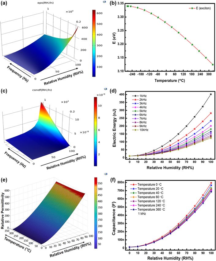
www.nature.com/scientificreports/
Figure 3. GaN sensing layer (a) Overall general scam spectrum, (b) Ga 3d band, (c) N 1s Band, and (d) O1s
band, (e) XRD, and (f) Raman spectrum.
Zu − Zl
SZ = (3)
RHu − RHl
Cu − Cl
SC = (4)
RHu − RHl
Here ‘Zu’ and ‘Zl’ are the upper and lower limits of the magnitude of impedance, ‘Cu’ and ‘Cl’ are upper and
lower limits of terminal capacitance, and ‘RHu’ and ‘RHl’ are the upper and lower limits of relative humidity. The
sensitivity is calculated as 79 kΩ/RH% and 8.53 nF/RH% for impedance and capacitance, respectively.
Transient response and stability analysis. Sensors are also characterized by transient response facili-
tating examination of response (Tres) and recovery (Trec) times upon sudden change for humidification and dehu-
midification process. A sudden increase in humidity through humidifier was analysed from 0 to 100% RH and
for dehumidification dry N2 gas was utilized for change from 100 to 0% RH. Response and recovery times for
impedance are calculated to be Tres ~ 3.5 s and Trec ~ 9 s, respectively and presented in Fig. 4c. Similarly, capaci-
Scientific Reports | (2021) 11:11088 | https://doi.org/10.1038/s41598-021-89956-0 5
Vol.:(0123456789)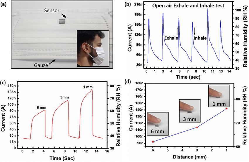
www.nature.com/scientificreports/

                                            Figure 4.  (a) Humidity test setup, (b) measured and simulated impedance and capacitance response at 1 kHz.
                                            (c) Impedance response and recovery. (d) Capacitance response and recovery. (e) Impedance stability, and (f)
                                            capacitance stability.

                                            tance response on time scale showing Tres ~ 11 s and Trec ~ 6 s, respectively are presented in Fig. 4d. Slow response
                                            and recovery time are attributed to chemical adsorption of hydronium and hydroxyl ions on GaN layer and
                                            considered a major drawback of GaN proposed sensor.
                                                Stability tests were performed on the proposed GaN sensor by observance of impedance and capacitance
                                            response under ambient conditions for 1 kHz frequency on different humidity levels (0%, 40%, and 100%) for
                                            consecutive 120 min as shown in Fig. 4e for impedance and Fig. 4f for capacitance response. The sensor presents
                                            a stable response with insignificant error over a wide range of change in impedance and capacitance responses.
                                            Hysteresis analysis at 1 kHz and 10 kHz frequencies are explained for both impedance and capacitance in supple-
                                            mentary Fig. S2. The frequency response of the sensor presented is discussed in detail in supplementary Fig. S3.
                                            Repeatability curves are explained in detail as shown in Fig. S4 of the supplementary information.

                                            Electrical conductivity and temperature stability. A glass substrate was designed with dimensions
                                            11 mm × 7 mm length and width, respectively. Susbtrate thickness was kept at 1 μm. A very thin layer of 300 nm
                                            thickness of GaN was formed on top of substrate. IDEs with finger width and spacing of 100 μm were formed
                                            on top of sensing layer. From materials library glass, GaN wurtzite, and silver were assigned as materials for
                                            substrate, sensing layer and IDEs, respectively. Simulations capacitance and impedance measurements are cal-
                                            culated from Eq. (5):

          Scientific Reports |   (2021) 11:11088 |               https://doi.org/10.1038/s41598-021-89956-0                                                    6

Vol:.(1234567890)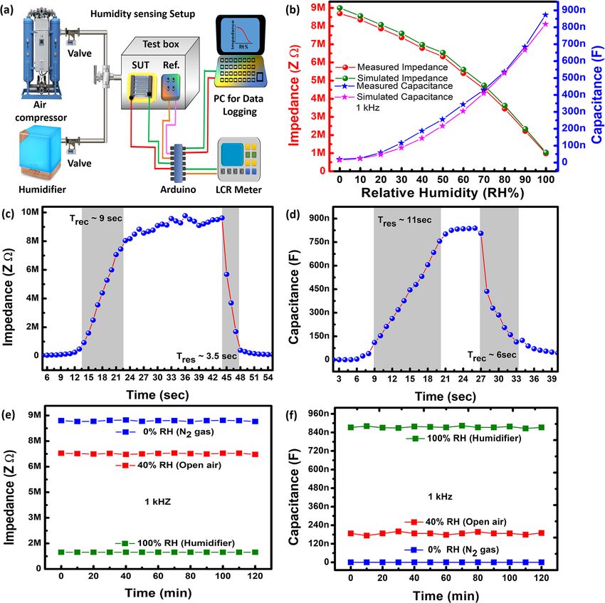
www.nature.com/scientificreports/

                                  Figure 5.  Simulation (a) relative permittivity w.r.t. frequency, (b) band gap energy w.r.t. temperature, (c)
                                  electrical conductivity w.r.t. frequency, (d) electric energy, (e) relative permittivity w.r.t. temperature, and (f)
                                  capacitance response w.r.t temperature variations.

                                                                                                            2
                                                                                                        1
                                                                                |Z| =       R2 +                                                         (5)
                                                                                                       2πfC

                                     Here, |Z| represents the impedance magnitude, f is the frequency at which measurements are made, C is the
                                  capacitance and R is the sheet resistance. Capacitive impedance and dielectric constant are frequency depend-
                                  ent. The complex permittivity decreases with increase in frequency this dependence is presented in Fig. 5a. As
                                  sensor structure consists of IDEs, the terminal capacitance is given by Eq. (6):
                                                                                              tl
                                                                                   C = nεr∗      = εr∗ Cinit                                             (6)
                                                                                              d

Scientific Reports |   (2021) 11:11088 |                https://doi.org/10.1038/s41598-021-89956-0                                                        7

                                                                                                                                                    Vol.:(0123456789)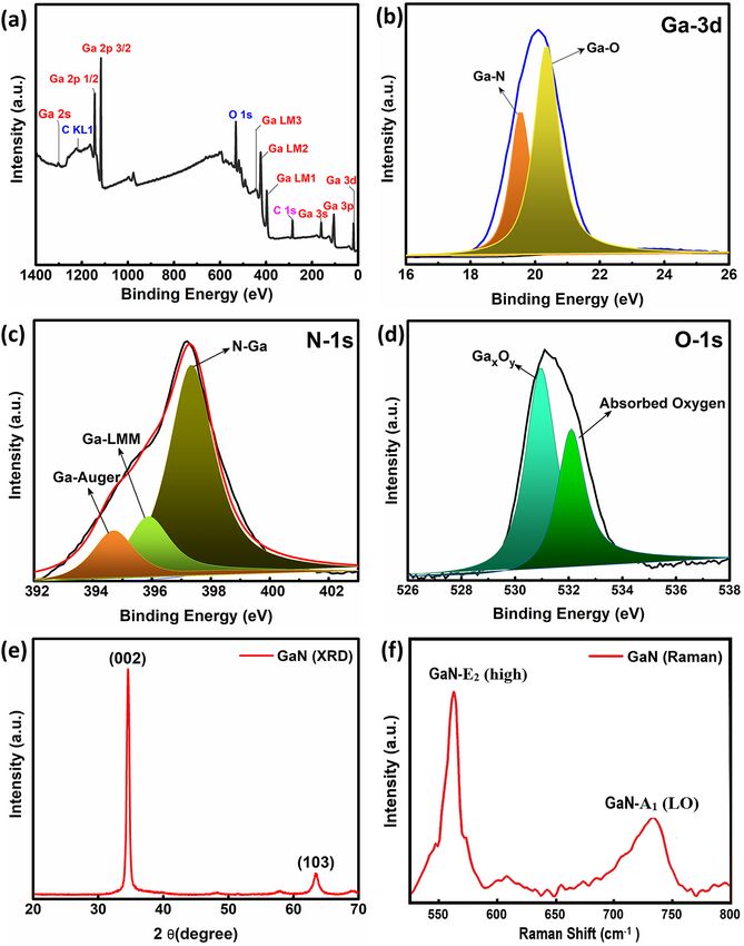
www.nature.com/scientificreports/
Here, n is the number of electrode fingers, t is the thickness or height, l is the overlapping length of individual
IDE, and d is the separation distance between them. εr∗ is the total change in permittivity. The dielectric of semi-
conductors also depends upon ambient temperature due to rearrangement of polarized ions. The temperature
dependence of energy band separation (E exciton) is calculated from Varshini e xpression42 and shown in Fig. 5b.
αT 2
E(T) = Ev − (7)
T +β
Here, Ev is the energy at − 273.15 °C temperature, T is the temperature, α, and β are constants with values
7.01 × 10⁻⁴ eV/K and 571 K
43. At 0 °C the band gap is observed at 3.287 eV. Thin film sheet resistance has direct
dependence upon material resistivity and is given in Eq. (8).
L
R=ρ (8)
A
Here, L is the length and A is the surface area. The L A ratio remains constant through experimentation.
Generally, resistivity can be calculated of a semiconductor from Eq. (9)44,45.
1
ρ=
(9)
q (nµn ) + pµp
Here, q is the electron charge, n and p represent the electron and hole concentrations and μn and μp represent
the electron and hole mobilities. From Eqs. (8) and (9) the resistivity and electrical conductivity of GaN are cal-
culated where reciprocal of resistivity in Eq. (10) gives the electrical conductivity of the material. Its frequency
dependent plot is shown in Fig. 5c.
1
σ = (10)
ρ
As frequency increases an increase in conductivity of GaN thin film occurs. The electric energy is related
to work done ‘W’ to store charges ‘Q’ on the electrode surfaces given by the Eq. (11) and presented in Fig. 5d
between frequency range of 1–10 kHz. The work done to store charge on electrodes is inversely dependent upon
capacitance of the sensor.
Q2
W= (11)
2C
The GaN is stable element and has low temperature dependence. This dependence is simulated between
range of 0–100% RH and temperature range of 0–360 °C, MATLAB plot is shown in Fig. 5e. Relative permittivity
changes from 600 to 583, on temperature variation from 25 to 360 °C. GaN is stable in a wide temperature range.
Figure 5f presents the simulated capacitance response at 0 °C, 20 °C, 40 °C, 60 °C, 120 °C, 240 °C, and 360 °C.
Sensing mechanism. Water auto-ionization is given by Eq. (12)46:
2H2 O → H3 O+ + OH − (12)
The water surface is much more acidic and hydronium ion is a strong proton donor. In presence of humid
conditions, the GaN surface oxides to G axOy making additional deficiencies providing more electrically active
sites for hydrogen atom adsorption47. Enhanced active sites increase the Fermi energy from semiconductor nature
of GaN towards conduction band. The adsorption of H2O causes the static dielectric constant of GaN ranging
between 8.9 and 9.748 to increase and hence an increase in capacitance is observed at the sensor terminals. The
chemical bonding of N H4+ and O H− is displayed in Fig. 6a. Upon energizing electrode terminals, a potential
difference is created between the electrodes as shown in 3D view in Fig. 6b, similarly cross-sectional view is
presented in Fig. 6c. The electrodes at higher potential are displayed in red while the low potential electrodes are
presented in blue. Thus, an electric field is created between the electrodes originating from the higher potential
surface and ending at low potential. A plot in 3D view is shown in Fig. 6d. The arrows present the direction
3O+ and O
of electric field is towards the ground electrode. This directional field aligns the H H− ions in a polar
molecular structure above the GaN layer. As RH increases, increase in adsorption of hydronium and hydroxyl
ions is observed resultantly the electric field intensity increases. Energizing the circuit through LCR meter the
parasitic capacitance between electrodes and substrate CPSE, sensing layer sheet resistance RSE, capacitance CSE
between the electrodes, capacitance due to adsorption of hydroxyl O H- ions on sensing layer CSVP and hydro-
nium ions H 3O+ ions CSVG are shown in the cross-sectional view in Fig. 6e. Both CSVP and CSVG have a parallel
capacitance effect. The change in ambient RH affects all the individual circuit elements present in the sensing
device. Thus, the measured change in impedance as well as capacitance is a cumulative effect. The equivalent
circuit thus formed follows Eq. (13)49 and a simplified circuit diagram is shown in Fig. 6f. Where, CS is the sen-
sor terminal capacitance.
CS = (CSVP � CSVG ) + CSE + CPSE (13)
Scientific Reports | (2021) 11:11088 | https://doi.org/10.1038/s41598-021-89956-0 8
Vol:.(1234567890)www.nature.com/scientificreports/
Figure 6. Sensing mechanism (a) chemical adsorption of water molecules on GaN sensing layer. Electrical
analysis (b) 3D view electric potential, (c) cross-sectional view electric potential, (d) 3D view of electric field
lines, (e) cross-sectional view of device layers, and (c) equivalent circuit.
A comparison is presented with GaN humidity sensors in Table 1. Majorly focusing on response and recovery
times, sensing range and sensor sensitivities. A sensor based on chemical etching and spray coating method was
developed4. The sheet resistance was tested as response to humidity. The sensing material used was porous GaN
with a limited sensing range of 0–60% RH with an average response and recovery time of 7 and 13 s, respectively.
Chemical vapour deposition method was used to fabricate GaN n anowires2, change is current was observed as
response towards humid conditions. The sensor shows a slightly higher range between 15 and 85% RH but a
slow response and recovery time of 22.59 and 26.16 s, respectively. A linear response dandelion like GaN nano-
flowers humidity sensor was demonstrated with a wide range of 11–97% RH50, measuring sheet impedance. Still
the response and recovery times are high. Fabrication of two sensors utilizing GaN powder G a2O3–Na–K doped
materials51 was demonstrated. For both the sensors impedance measurements were carried out. The measuring
Scientific Reports | (2021) 11:11088 | https://doi.org/10.1038/s41598-021-89956-0 9
Vol.:(0123456789)www.nature.com/scientificreports/
Refs. Fabrication method Sensing material Range (%) Response/recovery time (s) Sensitivity Sensor type
4 Chemical etching and spray
ZnO/Porous GaN 0–60 7/13 161 Diode formation
coating
2
Chemical vapor deposition Ni patterned GaN nanowire 15–85 22.59/26.16 Diode formation
50 3D dandelion like GaN
Dip coating 11–97 – 1000 Interdigitated electrodes
flower
51
Spin coating GaN Powder 75–95 – – Interdigitated electrodes
51
Spin coating Ga2O3-Na–K Doped 10–85 6/21 500 Interdigitated electrodes
16 β-Ga2O3 nanowires on GaN
MOCVD 35–95 25/45 30 Resistive sheet formation
substrate
1 Chemical method etching
GaN nanoparticles 4–84 140/130 105 –
from GaCl3
17 β-Ga2O3 nanowires on GaN 24.94/6.24 @ 30% RH 319 in dark
MOCVD 30–90 Interdigitated electrodes
substrate 1.36/1.8 @ 90% RH 7.3 in UV
Pulsed DC magnetron sput- ZnO buffer layer/GaN thin Impedance 3.5/9 79 kΩ/RH%
This work 0–100 (Linear response) Interdigitated electrodes
tering and inkjet printing film Capacitance 11/6 8.53 nF/RH%
Table 1. Comparison table of GaN humidity sensors.
ranges of 75–95% RH and 10–85% RH were observed with a response and recovery time of 6 and 21 s, respec-
tively. The sensitivity of the sensor was directly dependent upon the doping concentrations of Sodium Na and
Potassium K ions. G umidity16,
a2O3 based nanowires on GaN substrate, sheet resistance was tested as response to h
the sensor shows a limited range of detection between 35 and 95% RH with slow response and recovery times,
the proposed sensor also shows low sensitivity towards ambient humidity levels. GaN nanoparticles based sen-
sor was fabricated1, sheet resistance was tested as response to humidity. The response and recovery time of 140
and 130 s were observed, respectively. G a2O3 based sensor measuring the sheet resistance was prepared17, with
a limited detection range of 30–90% RH. The proposed sensor not only has an approximate linear response
towards ambient humid conditions, but also caters the all range of detection between 0 and 100% RH, showing
a higher capacitive and impedance sensitivity of ~ 8.53 nF/RH%, and ~ 79 kΩ/RH%, respectively. Maintaining
a considerably short response and recovery time of ~ 3.5 and ~ 9 s, respectively.
Applications
For bio sensing applications a DC bias was applied of 5 V on electrode terminals using KEYSIGHT B2902A
source measurement unit apparatus to measure the flow of DC current, while an Arduino was connected with
reference ammonia sensor TGS2602 for meat freshness test. Both the B2902A source measurement unit as well
as Arduino were connected to a computer via USB(s) for data logging.
Breathing rate and proximity analysis. The proposed sensor was integrated into a mask for real time
monitoring of human breath as shown in Fig. 7a. The average breathing rate at rest in adults is 12–18 breaths/
min. Air current from breath are used to detect transient response. Exhaling / humidification process can reach
up to 100% RH decreasing the sheet resistance, while inhaling/dehumidification process can reach as low as 35%
RH increasing the sheet resistance. Figure 7b shows the transient response, current shifts from 35 to 195 nA for
exhaling, while inhaling a current drop is observed from a peak 195–38 nA. The hypersensitive vapor response
of GaN sensor allows its utility in applications like proximity analysis. The humidity sensor shows a rapid real-
time change of current after placing a wet finger at distances of 1 mm, 3 mm, and 6 mm above the device. The
currents are measured as 135 nA, 118 nA, and 90 nA at distances of 1 mm, 3 mm, and 6 mm, respectively as
shown in Fig. 7c and d. The proposed sensing layer absorbs moisture from surface of bare fingertip, while sensor
shows no response to covered fingertip brought closer to the sensor surface.
Plant transpiration monitoring. Plant growth rate is directly linked to its’ water status, drought condi-
tions can inhibit growth rate of a plant3. The sensor was attached to backside of leaf as shown in Fig. 8a and
capacitance response was recorded from 1 to 5 days as shown in Fig. 8b. To perform drought conditions, long
term capacitive measurements were performed to estimate water quantity of soil. A picture of attached sensor
to leaf is shown in Fig. 8a, the zoomed image shows the cross-sectional view of leaf. The data was recorded for
5 days with sampling after 24 h, at 1 day addition of water to soil increased the uptake and release of water mol-
ecules from stomata corresponding to increase in capacitance at 1 day as shown in Fig. 8b. A drop in capacitance
is observed as days pass by due to water evaporation from soil corresponding to decrease in capacitance shown
in Fig. 8b. These results indicate that proposed can be employed for smart agriculture.
Meat quality test. Fresh meat was purchased from local market and placed on same day in test chamber.
Meat proteins are formed by long chains of amino acids and general structure of proteins is shown in Fig. 8c.
Meat decomposition starts by secretion of decomposing enzymes by bacteria’s. A particular type of amino acid
known as l-Cysteine structure is presented in the Fig. 8c. Cystathionine-γ -lyase secreted by bacteria decom-
posed Cysteine into Pyruvate releasing ammonia (NH3) and hydrogen sulfide (H2S) gases. Ammonia like water
Scientific Reports | (2021) 11:11088 | https://doi.org/10.1038/s41598-021-89956-0 10
Vol:.(1234567890)www.nature.com/scientificreports/
Figure 7. (a) Integration of sensor onto the mask, inset shows volunteer wearing the mask, (b) current response
to human breathing, (c) time varying current response to approaching finger, and (d) measurements of sensor at
different distances, insets photographs of finger approaching sensor surface.
auto-ionizes as well as dissolves in water to form ammonium and hydroxyl ions. These reactions are presented
in Eqs. (14) and (15).
2NH3 ↔ NH4+ + NH2− (14)
NH3 + H2 O → NH4+ + OH − (15)
As the decomposition rate increases so does the concentration of ammonia as well as ammonium and
hydroxyl ions in test chamber decreasing GaN sheet resistance. A 100 h duration test was conducted keeping
ambient temperature at 25 °C and 40% RH level inside the test jar with sampling time of 10 h. In the first 24 h,
the response of the sensor was quite small with little ammonia accumulation. The current response of the sen-
sor stays below 110 nA till 24 h as shown in Fig. 8d categorized as fresh. The spoilage of meat started after 24 h
due to rapid growth of microbes till 65 ppm ammonia accumulation categorized as semi fresh. After spoilage,
the current response of the sensor reaches 180 nA with high ammonia concentration of 105 ppm categorized as
spoiled meat. The results indicate the effectiveness of the sensor making it suitable for freshness evaluation. The
results were divided into three sections as fresh, semi-fresh and spoiled according to human sensory evaluation
to distinguish between freshness levels as shown in Fig. 8d based on odor and color during the spoilage process.
Most recent works on humidity sensors based on temperature dependence, biocompatibility and response
linearity are presented in Table 2. A highly nonlinear and temperature sensitive but biocompatible humidity
sensor was demonstrated via drop casting of graphene oxide aqueous solution on polyethylene terephthalate
(PET) substrate3. The capacitive sensor shows a high sensitivity of ~ 3215 pF between sensing range of 10 to
90% RH. Three sensors were fabricated through chemical vapor deposition method with biocompatibility and
temperature independence based on porous graphene oxide, graphene oxide immersed in PEDOT:PSS solu-
tion, and graphene oxide immersed in silver (Ag) colloidal solution52. However, the resistive sensor shows slight
nonlinearity and slow response time towards high humidity ranges above 50% RH as well as low sensitivity of
~ 3.21%. Fastest response and recovery time among these sensors achieved were 31 s and 72 s. A temperature
dependent and bio-incompatible sensor was developed based on Ag–SnO2 with a good detection range of 20–80%
RH having linear response53 through spin coating and thermal evaporation process. Managed to demonstrate
and monitor fish meat quality even though the sensor itself is bio-incompatible. Superfast response and recov-
ery time sensors were fabricated, practically utilizable in real time applications based on MPOSS-PIL54 through
drop casting, PEDOT:PSS, Methyl Red and Graphene oxide in series c ombination13 via spin coating, M oS2 and
PEDOT:PSS in series c ombination55 through SAW-EHDA deposition. All these sensors maintained a very wide
range detection with approximate linear response curves. The major drawback of these sensors is high ambient
temperature dependence. In comparison to all these recent and substantial efforts, this work presents all range
humidity detection from 0 to 100% RH with an approximate linear response and low temperature dependence.
Scientific Reports | (2021) 11:11088 | https://doi.org/10.1038/s41598-021-89956-0 11
Vol.:(0123456789)www.nature.com/scientificreports/
Figure 8. (a) Picture of sensor attached at lower side of plant leaf and cross-sectional view of leaf with sensing
mechanism and (b) real time monitoring of capacitive response towards plant transpiration after water from 1 to
5 days. Meat freshness test: (c) Amino acids structure and decomposition mechanism and (d) current response
w.r.t. time and freshness states.
Refs Sensing material Range (%) Curve shape Temperature dependency Biocompatibility Applications
3 Breathing rate and plant transpiration
Graphene oxide solution 10–90 Highly Non linear Highly dependent Compatible
monitoring
Porous graphene/graphene oxide; gra-
52
phene oxide and PEDOT;PSS; porous 12–97 Non linear Independent Compatible Breathing rate monitoring
graphene and Ag colloids
53
Ag-SnO2 20–80 Slightly linear Highly dependent Incompatible Fish quality monitoring
54
MPOSS-PIL 11–95 Slightly linear – (Seems dependent) – Breath monitoring
13 PEDOT:PSS, methyl red and graphene
0–100 Approximate linear Highly dependent Compatible –
oxide in series
55
MoS2 and PEDOT:PSS in series 0–80 Approximate linear Highly dependent Compatible –
Plant transpiration and meat quality
This Work ZnO buffer layer/GaN thin film 0–100 Approximate linear Slightly dependent Compatible
monitoring
Table 2. Comparison table of biocompatible humidity sensors.
The proposed sensor shows fast response and recovery times of ~ 3.5 s and ~ 9 s. The proposed sensor is biocom-
patible favorable for bio-sensing applications.
Conclusion
This work reports highly linear humidity sensor based on GaN as sensing layer, fabricated through sputtering
technology and silver IDEs via inkjet printing process. The proposed sensor shows impedance sensitivity ~ 79
kΩ/RH% and capacitance sensitivity ~ 8.53 nF/RH% in a range between 0 and 100% RH with hysteresis response
< 3.53% and Tres ~ 3.5 s and Trec ~ 9 s. Sensor shows stable humidity response on temperature variation in a range
Scientific Reports | (2021) 11:11088 | https://doi.org/10.1038/s41598-021-89956-0 12
Vol:.(1234567890)www.nature.com/scientificreports/
of 0–360 °C. The sensor performance was validated through computer aided simulations. The higher stability
and reliability of GaN makes its utility in real life applications, which include breath monitoring, proximity test,
meat freshness test and plant water level monitoring.
Received: 28 October 2020; Accepted: 23 April 2021
References
1. Chitara, B., Late, D. J., Krupanidhi, S. & Rao, C. Room-temperature gas sensors based on gallium nitride nanoparticles. Solid State
Commun. 150, 2053–2056. https://doi.org/10.1016/j.ssc.2010.08.007 (2010).
2. Peng, M. et al. Ni-pattern guided GaN nanowire-array humidity sensor with high sensitivity enhanced by UV photoexcitation.
Sens. Actuators B Chem. 256, 367–373. https://doi.org/10.1016/j.snb.2017.10.077 (2018).
3. Lan, L. et al. One-step and large-scale fabrication of flexible and wearable humidity sensor based on laser-induced graphene for
real-time tracking of plant transpiration at bio-interface. Biosens. Bioelectron. https://doi.org/10.1016/j.bios.2020.112360 (2020).
4. Wang, C. et al. A ZnO/porous GaN heterojunction and its application as a humidity sensor. Nanoscale Adv. 1, 1232–1239. https://
doi.org/10.1039/C8NA00243F (2019).
5. Khan, M. U., Hassan, G., Awais, M. & Bae, J. All printed full range humidity sensor based on F e2O3. Sens. Actuators A Phys. https://
doi.org/10.1016/j.sna.2020.112072 (2020).
6. Hassan, G., Bae, J., Lee, C. H. & Hassan, A. Wide range and stable ink-jet printed humidity sensor based on graphene and zinc
oxide nanocomposite. J. Mater. Sci. Mater. Electron. 29, 5806–5813. https://doi.org/10.1007/s10854-018-8552-z (2018).
7. Yang, S., Jiang, C. & Wei, S.-H. Gas sensing in 2D materials. Appl. Phys. Rev. 4, 021304. https://doi.org/10.1063/1.4983310 (2017).
8. Zhao, J. et al. Highly sensitive M oS2 humidity sensors array for noncontact sensation. Adv. Mater. 29, 1702076. https://doi.org/10.
1002/adma.201702076 (2017).
9. He, P. et al. Fully printed high performance humidity sensors based on two-dimensional materials. Nanoscale 10, 5599–5606.
https://doi.org/10.1039/C7NR08115D (2018).
10. Chaudhary, P. et al. Ultrafast responsive humidity sensor based on roasted gram derived carbon quantum dots: experimental and
theoretical study. Sens. Actuators B Chem. 329, 129116. https://doi.org/10.1016/j.snb.2020.129116 (2021).
11. Awais, M., Khan, M. U., Hassan, A., Bae, J. & Chattha, T. E. Printable highly stable and superfast humidity sensor based on two
dimensional molybdenum diselenide. Sci. Rep. 10, 1–13. https://doi.org/10.1038/s41598-020-62397-x (2020).
12. Khan, M. U., Awais, M., Chattha, T. E., Hassan, A. & Bae, J. All printed wide range humidity sensor array combining M oSe2 and
PVOH in series. J. Mater. Sci. Mater. Electron. https://doi.org/10.1007/s10854-020-03304-y (2020).
13. Hassan, G., Sajid, M. & Choi, C. Highly sensitive and full range detectable humidity sensor using PEDOT: PSS, methyl red and
graphene oxide materials. Sci. Rep. 9, 1–10. https://doi.org/10.1038/s41598-019-51712-w (2019).
14. Ali, S., Hassan, A., Hassan, G., Bae, J. & Lee, C. H. All-printed humidity sensor based on graphene/methyl-red composite with
high sensitivity. Carbon 105, 23–32. https://doi.org/10.1016/j.carbon.2016.04.013 (2016).
15. Khan, M. A. H., Thomson, B., Motayed, A., Li, Q. & Rao, M. V. Functionalization of GaN Nanowire sensors with metal oxides: an
experimental and DFT investigation. IEEE Sens. J. https://doi.org/10.1109/JSEN.2020.2978221 (2020).
16. Tsai, T.-Y. et al. β-Ga2O3 Nanowires-based humidity sensors prepared on GaN/sapphire substrate. IEEE Sens. J. 13, 4891–4896.
https://doi.org/10.1109/JSEN.2013.2274872 (2013).
17. Juan, Y. et al. Effects of humidity and ultraviolet characteristics on β-Ga2O3 nanowire sensor. RSC Adv. 5, 84776–84781. https://
doi.org/10.1039/C5RA16710H (2015).
18. Greenwood, N. Advances in Inorganic Chemistry and Radiochemistry Vol. 5, 91–134 (Elsevier, 1963).
19. Chaniotakis, N. & Sofikiti, N. Novel semiconductor materials for the development of chemical sensors and biosensors: a review.
Anal. Chim. Acta 615, 1–9. https://doi.org/10.1016/j.aca.2008.03.046 (2008).
20. Bui, Q. C. et al. GaN/Ga2O3 core/shell nanowires growth: nanostructures for future CO-sensors developments. Appl. Sci. https://
doi.org/10.3390/app9173528 (2019).
21. Mishra, U. K., Parikh, P. & Wu, Y.-F. AlGaN/GaN HEMTs-an overview of device operation and applications. Proc. IEEE 90,
1022–1031. https://doi.org/10.1109/JPROC.2002.1021567 (2002).
22. Yong, Y. et al. Adsorption of gas molecules on a graphitic GaN sheet and its implications for molecule sensors. RSC Adv. 7,
51027–51035. https://doi.org/10.1039/C7RA11106A (2017).
23. Young, T.-H. & Chen, C.-R. Assessment of GaN chips for culturing cerebellar granule neurons. Biomaterials 27, 3361–3367. https://
doi.org/10.1016/j.biomaterials.2006.02.001 (2006).
24. Podolska, A. et al. Biocompatibility of semiconducting AlGaN/GaN material with living cells. Sens. Actuators B Chem. 169,
401–406. https://doi.org/10.1016/j.snb.2012.04.015 (2012).
25. Sprenger, J. K. et al. Electron enhanced growth of crystalline gallium nitride thin films at room temperature and 100 C using
sequential surface reactions. Chem. Mater. 28, 5282–5294. https://doi.org/10.1021/acs.chemmater.6b00676 (2016).
26. Denis, A., Goglio, G. & Demazeau, G. Gallium nitride bulk crystal growth processes: a review. Mater. Sci. Eng. R Rep. 50, 167–194.
https://doi.org/10.1016/j.mser.2005.11.001 (2006).
27. Karpiński, J., Jun, J. & Porowski, S. Equilibrium pressure of N 2 over GaN and high pressure solution growth of GaN. J. Cryst. Growth
66, 1–10. https://doi.org/10.1016/0022-0248(84)90070-8 (1984).
28. Kylián, O. et al. Magnetron sputtering of polymeric targets: from thin films to heterogeneous metal/plasma polymer nanoparticles.
Materials 12, 2366. https://doi.org/10.3390/ma12152366 (2019).
29. Kelly, P., Hisek, J., Zhou, Y., Pilkington, R. & Arnell, R. Advanced coatings through pulsed magnetron sputtering. Surf. Eng. 20,
157–162. https://doi.org/10.1179/026708404225010702 (2004).
30. Kelly, P. J. & Arnell, R. D. Magnetron sputtering: a review of recent developments and applications. Vacuum 56, 159–172. https://
doi.org/10.1016/S0042-207X(99)00189-X (2000).
31. Swann, S. Magnetron sputtering. Phys. Technol. 19, 67. https://doi.org/10.1088/0305-4624/19/2/304 (1988).
32. Black, J. T. & Kohser, R. A. DeGarmo’s Materials and Processes in Manufacturing (Wiley, 2017).
33. Griffiths, BScience (Penton Press).
34. Martin, G., Botchkarev, A., Rockett, A. & Morkoc, H. Valence-band discontinuities of wurtzite GaN, AlN, and InN heterojunctions
measured by X-ray photoemission spectroscopy. Appl. Phys. Lett. 68, 2541–2543. https://doi.org/10.1063/1.116177 (1996).
35. Benemanskaya, G., Pronin, V., Timoshnev, S. & Nelyubov, A. Soft X-ray photoelectron spectroscopy of the ultrathin Ba/InGaN
interface. Appl. Surf. Sci. 423, 1198–1202. https://doi.org/10.1016/j.apsusc.2017.07.013 (2017).
36. Chen, R. et al. Investigation of top gate GaN thin-film transistor fabricated by DC magnetron sputtering. J. Vac. Sci. Technol. B
Nanotechnol. Microelectron. Mater. Process. Meas. Phenom. 36, 032203. https://doi.org/10.1116/1.5021705 (2018).
37. Puech, P. et al. GaN nanoindentation: a micro-Raman spectroscopy study of local strain fields. J. Appl. Phys. 96, 2853–2856. https://
doi.org/10.1063/1.1775295 (2004).
Scientific Reports | (2021) 11:11088 | https://doi.org/10.1038/s41598-021-89956-0 13
Vol.:(0123456789)www.nature.com/scientificreports/
38. Chiu, C.-H. et al. High efficiency GaN-based light-emitting diodes with embedded air voids/SiO2 nanomasks. Nanotechnology 23,
045303. https://doi.org/10.1088/0957-4484/23/4/045303 (2012).
39. Khan, M., Saqib, Q. M., Hassan, G. & Bae, J. All printed organic humidity sensor based on egg albumin. Sens. Bio-Sens. Res. https://
doi.org/10.1016/j.sbsr.2020.100337 (2020).
40. Khan, M. U., Hassan, G. & Bae, J. Bio-compatible organic humidity sensor based on natural inner egg shell membrane with mul-
tilayer crosslinked fiber structure. Sci. Rep. 9, 5824. https://doi.org/10.1038/s41598-019-42337-0 (2019).
41. Kumar, L., Islam, T. & Mukhopadhyay, S. Sensitivity enhancement of a PPM level capacitive moisture sensor. Electronics 6, 41.
https://doi.org/10.3390/electronics6020041 (2017).
42. Varshni, Y. P. Temperature dependence of the energy gap in semiconductors. Physica 34, 149–154. https://doi.org/10.1016/0031-
8914(67)90062-6 (1967).
43. Kim, T. J. et al. Analytic representation of the dielectric function of GaN for temperatures from 26 to 690 K. J. Korean Phys. Soc.
65, 733–738. https://doi.org/10.3938/jkps.65.733 (2014).
44. Saini, D. K. Gallium nitride: Analysis of Physical Properties and Performance in High-Frequency Power Electronic Circuits. Master
of Science thesis, Wright State University (2015).
45. Bolat, S. Electrical Properties and Device Applications of Atomic Layer Deposited ZnO and GaN Thin Films. Master of Science thesis,
Bilkent University, (2014).
46. Buch, V., Milet, A., Vácha, R., Jungwirth, P. & Devlin, J. P. Water surface is acidic. Proc. Natl. Acad. Sci. 104, 7342–7347. https://
doi.org/10.1073/pnas.0611285104 (2007).
47. Chen, C.-C. et al. On a GaN-based ion sensitive field-effect transistor (ISFET) with a hydrogen peroxide surface treatment. Sens.
Actuators B Chem. 209, 658–663. https://doi.org/10.1016/j.snb.2014.12.025 (2015).
48. Bougrov, V., Levinshtein, M., Rumyantsev, S. L. & Zubrilov, A. Properties of Advanced Semiconductor Materials GaN, AlN, InN,
BN, SiC, SiGe. Bougrov, ME Levinshtein, SL Rumyantsev, A. 1–50 (Wiley, 2001).
49. Ghafar-Zadeh, E., Sawan, M., Ghafar-Zadeh, E. & Sawan, M. CMOS Capacitive Sensors for Lab-on-Chip Applications (Springer,
2010).
50. Veerappan, M., Leng, X., Rajendran, R. & Wang, F. in 2019 20th International Conference on Solid-State Sensors, Actuators and
Microsystems & Eurosensors XXXIII (TRANSDUCERS & EUROSENSORS XXXIII). 1690–1693 (IEEE).
51. Wang, D. et al. Humidity sensor based on G a2O3 nanorods doped with Na+ and K+ from GaN powder. Ceram. Int. 41, 14790–
14797. https://doi.org/10.1016/j.ceramint.2015.07.211 (2015).
52. Pang, Y. et al. Wearable humidity sensor based on porous graphene network for respiration monitoring. Biosens. Bioelectron. 116,
123–129. https://doi.org/10.1016/j.bios.2018.05.038 (2018).
53. Senapati, M. & Sahu, P. P. Onsite fish quality monitoring using ultra-sensitive patch electrode capacitive sensor at room temperature.
Biosens. Bioelectron. 168, 112570. https://doi.org/10.1016/j.bios.2020.112570 (2020).
54. Dai, J. et al. Design strategy for ultrafast-response humidity sensors based on gel polymer electrolytes and application for detecting
respiration. Sens. Actuators B Chem. 304, 127270. https://doi.org/10.1016/j.snb.2019.127270 (2020).
55. Siddiqui, G. U. et al. Wide range highly sensitive relative humidity sensor based on series combination of MoS2 and PEDOT: PSS
sensors array. Sens. Actuators B Chem. 266, 354–363. https://doi.org/10.1016/j.snb.2018.03.134 (2018).
Acknowledgements
This project was supported by State Key Laboratory on Advanced Displays and Optoelectronics Technologies
from The Hong Kong University of Science and Technology and National Research Foundation of Korea (NRF)
grant funded by the Korean government (MSIP) 2020R1A2C1011433.
Author contributions
C.M.F., M.U.K. and M.A. are considered first authors with equal proportions. C.M.F. and F.J. executed deposition
of sensing layer and performed structural characterization of GaN. M.U.K. fabricated the sensor and performed
the surface morphological characterization. M.U.K. developed the experimental setups, executed the tests and
recorded the results. M.A. mathematically modelled, performed the simulations. C.M.F., M.U.K. and M.A. pre-
pared manuscript draft. J.B., A.H., and H.S.K. supervised the research.
Competing interests
The authors declare no competing interests.
Additional information
Supplementary Information The online version contains supplementary material available at https://doi.org/
10.1038/s41598-021-89956-0.
Correspondence and requests for materials should be addressed to J.B., A.H. or H.-S.K.
Reprints and permissions information is available at www.nature.com/reprints.
Publisher’s note Springer Nature remains neutral with regard to jurisdictional claims in published maps and
institutional affiliations.
Open Access This article is licensed under a Creative Commons Attribution 4.0 International
License, which permits use, sharing, adaptation, distribution and reproduction in any medium or
format, as long as you give appropriate credit to the original author(s) and the source, provide a link to the
Creative Commons licence, and indicate if changes were made. The images or other third party material in this
article are included in the article’s Creative Commons licence, unless indicated otherwise in a credit line to the
material. If material is not included in the article’s Creative Commons licence and your intended use is not
permitted by statutory regulation or exceeds the permitted use, you will need to obtain permission directly from
the copyright holder. To view a copy of this licence, visit http://creativecommons.org/licenses/by/4.0/.
© The Author(s) 2021
Scientific Reports | (2021) 11:11088 | https://doi.org/10.1038/s41598-021-89956-0 14
Vol:.(1234567890)You can also read