Insights into Improving Performance of Niobium Superconducting Transmon Qubit Devices through Advanced Microscopy
←
→
Page content transcription
If your browser does not render page correctly, please read the page content below
Insights into Improving Performance of Niobium Superconducting Transmon Qubit
                                                                           Devices through Advanced Microscopy

                                                               Akshay A. Murthy1∗ , Paul Masih Das2 , Stephanie M. Ribet2,3 , Cameron Kopas4 , Jaeyel Lee1 ,
                                                               Matthew J. Reagor4 , Lin Zhou5 , Matthew J. Kramer5 , Mark C. Hersam2,6,7 , Mattia Checchin1 ,
                                                                Anna Grassellino1 , Roberto dos Reis2,3,8 , Vinayak P. Dravid2,3,8∗ , Alexander Romanenko1∗
                                                                                     1
                                                                                        Superconducting Quantum Materials and Systems Division,
                                                                                Fermi National Accelerator Laboratory (FNAL), Batavia, IL 60510, USA
                                                                                            2
                                                                                              Department of Materials Science and Engineering,
                                                                                            Northwestern University, Evanston, IL 60208, USA
arXiv:2203.08710v2 [cond-mat.mes-hall] 23 May 2022

                                                                   3
                                                                     International Institute of Nanotechnology, Northwestern University, Evanston, IL 60208, USA
                                                                                               4
                                                                                                 Rigetti Computing, Berkeley, CA 94710, USA
                                                                           5
                                                                             Ames Laboratory, U.S. Department of Energy, Ames, IA 50011, United States
                                                                                6
                                                                                  Department of Chemistry, Northwestern University, Evanston, IL 60208
                                                                                          7
                                                                                            Department of Electrical and Computer Engineering,
                                                                                               Northwestern University, Evanston, IL 60208 ,
                                                                             8
                                                                               The NUANCE Center, Northwestern University, Evanston, IL 60208, USA
                                                                                                            (Dated: May 25, 2022)
                                                                     Superconducting thin films of niobium have been extensively employed in transmon qubit ar-
                                                                  chitectures. Although these architectures have demonstrated remarkable improvements in recent
                                                                  years, further improvements in performance through materials engineering will aid in large-scale
                                                                  deployment. Here, we use information retrieved from electron microscopy to conduct a detailed
                                                                  assessment of defects and inhomogeneities on the atomic and nanoscale that may potentially induce
                                                                  quantum decoherence in transmon qubit test devices. In the niobium thin film, we observe the
                                                                  presence of localized strain at the metal/substrate and grain boundaries, which may amplify inter-
                                                                  actions between two-level systems and impose limits on T1 and T2 relaxation times. Additionally,
                                                                  we observe the presence of a surface oxide with varying stoichiometry and bond distances, which
                                                                  can generate a broad two-level system noise spectrum. Finally, a similarly disordered and rough
                                                                  interface is observed between Nb and the Si substrate. We propose that this interface can also
                                                                  degrade the overall superconducting properties. Based on these findings, we propose solutions to
                                                                  eliminate these potentially problematic imperfections in future quantum devices.
                                                                  Keywords: superconducting qubits, 4D-STEM, electron diffraction, Nb thin films, interfaces, hydrides, de-
                                                                  coherence mechanisms

                                                       Over the last two decades, many significant advances             nitude larger compared to the Nb thin films and Si
                                                     have been made towards constructing large-scale quan-              substrates [6–8]. This loss can be largely attributed
                                                     tum computers. In particular, superconducting quan-                to two-state defects in the amorphous surface oxide,
                                                     tum information technology has emerged as a lead-                  i.e. two-level system (TLS) defects [6]. These states
                                                     ing architecture to interrogate complex problems com-              emerge as a result of deviations from long-range order.
                                                     monly deemed intractable with the most efficient classi-           The system is able to transition between the two states
                                                     cal computing platforms [1–4]. Nonetheless, extending              through low energy excitations at the operating tem-
                                                     this technology to large-scale devices requires contin-            peratures for superconducting transmon qubits [9, 10].
                                                     ued progress to improve reliability and performance.               Similarly, the presence of grain boundaries within the
                                                     Such improvements require higher quality materials                 Nb film decreases mean free paths and superconducting
                                                     and specifically, an increased understanding and control           parameters, such as the residual-resistance ratio (RRR),
                                                     over imperfections including interfaces and surfaces [5].          which can also lead to diminished T1 energy relaxation
                                                       As an example, in the case of niobium (Nb)-                      decoherence times [9]. As a result, it is important to un-
                                                     superconducting transmon qubits, the amorphous sur-                derstand the form-function relationships between pro-
                                                     face oxides that form upon ambient exposure serve as               cessing parameters and structure and concentration of
                                                     major sources of electromagnetic energy dissipation. At            TLS defects in these materials.
                                                     milliKelvin (mK) operating temperatures, they also dis-
                                                     play loss tangent values that are three orders of mag-               A combination of various spectroscopy and mi-
                                                                                                                        croscopy techniques have led researchers to understand
                                                                                                                        that deviations from crystalline range order on the
                                                                                                                        nanoscale dictate quantum decoherence [10]. As such,
                                                     ∗   Correspondence email address:      amurthy@fnal.gov,     v-    scanning transmission electron microscopy (STEM) is
                                                         dravid@northwestern.edu, aroman@fnal.gov                       an indispensable tool for identification of materials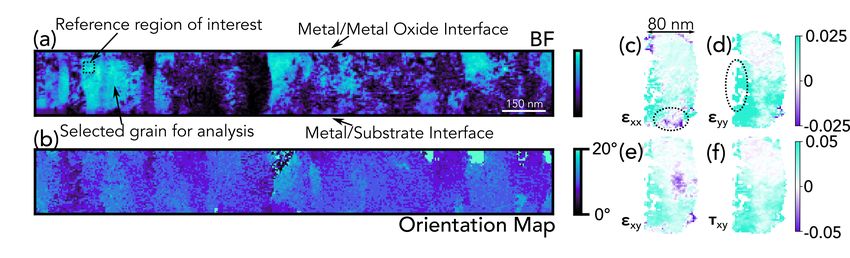
2

Figure 1. Nb/Si interface (a) Schematic of transmon qubit       Figure 2. Nb film structure (a) Bright field and (b) Rela-
architecture. Black box represents the Nb contact pad re-       tive in-plane orientation map of Nb grains. Relative magni-
gion investigated in this study. (b) Annular dark field image   tudes of the strain present in an on-axis Nb grain are pro-
taken from the cross-sectional TEM sample. The metal/air        vided (c) along the substrate axis (xx ) and (d) along the
and metal/substrate interfaces discussed in Sections and        film growth axis (yy ). Regions of compressive strain at the
are indicated. (c) EDS maps taken from the region indi-         metal/substrate interface and tensile strain near the grain
cated by the white box in (b) using characteristic Nb Lα        boundary are circled. Shear strain in the sample plane (xy )
and Si Kα x-ray emission.                                       along with rotational strain in the sample plane (τxy ) are
                                                                provided in (e) and (f) respectively. The selected grain and
                                                                unstrained reference regions are also indicated.
that host TLS defects in a broader effort to eliminate
these sources. Namely, the ability to procure a vari-
ety of analytical and spectroscopic signals from nano-          to 70 mrad is provided in Figure 1b. In Figure 1c,
metric volumes allows for detection of chemical, struc-         an elemental map taken from this region using energy
tural, and electromagnetic fluctuations on these rele-          dispersive x-ray spectroscopy (EDS) confirms the pres-
vant length scales [11, 12]. We deploy STEM imaging             ence of a Nb film on a Si substrate. In Figure 2a and
and diffraction methods to pinpoint specific nanoscale          b, bright field (BF) images taken when tilted along the
defects in the Nb film and associated surfaces and inter-       Nb {111} zone axis are provided. From this image, we
faces within a transmon qubit test device. The use of           observe that columnar grains form, which are charac-
cutting edge techniques to disentangle amorphous and            teristic of the HiPIMS process, and are roughly 50 nm
crystalline features allows us to observe a number of           by 170 nm. It is also apparent that many of the grains
structural and chemical features in this system that can        are not oriented along this zone axis. In fact, from the
potentially serve as hosts for TLS and reduce perfor-           orientation map, the grains tend to exhibit misorienta-
mance. These include the presence of localized strain           tion angles between 0 and 20 degrees from the Nb {111}
at interfaces, variation in bond distances in the disor-        zone axis in the sample plane. These columnar grains
dered surface oxide layer, as well as a rough and diffuse       are separated by grain boundaries that exist parallel to
metal/substrate interface.                                      the film growth axis.
   Nb transmon test qubits were fabricated following               Although a variety of chemical and physical prop-
the procedures detailed by Nersisyan et al. [13] This           erties contribute to BF contrast, strain is the domi-
involved preparation of a Si (001) wafer (float-zone            nant mechanism in this case due to large differences
>10,000 Ohm-cm) with an RCA surface treatment                   in the lattice constant between the metal and underly-
[13, 14], followed by deposition of Nb films via high-          ing substrate. In order to visualize these strained areas
power impulse magnetron sputtering (HiPIMS) with a              more clearly, we performed strain analysis using the al-
base pressure less than 1E-8 Torr at room temperature.          gorithm detailed by Pekin et al [15]. Strain within a
TEM samples were prepared from the Nb capacitance               crystalline sample leads to small atomic shifts in real
pad indicated with the black box in Figure 1a using             space, which manifest in shifts to the diffraction pat-
a 30 kV focused Ga+ ion beam. We first provide an               tern in reciprocal space. These shifts to the diffraction
assessment of the nanostructure and strain distribution         pattern can be measured and linked to relative in-plane
in the Nb thin film before searching for nanoscale inho-        strain in the sample through a transformation matrix.
mogeneities in surfaces and interfaces associated with          This approach is advantageous over direct real space
Nb.                                                             mapping because it does not require the resolution and
                                                                signal to noise necessary for atomic resolution imaging.
                                                                The resultant maps of the strain magnitudes along var-
    INTERFACES AND STRAIN GRADIENTS IN                          ious directions are provided in Figures 2c-f for a repre-
               NIOBIUM FILM                                     sentative grain oriented perfectly along the zone axis.
                                                                   Along the substrate axis (xx ), we observe the pres-
  An annular dark field (ADF) image of the cross-               ence of compressive strain at the metal/substrate in-
section taken from the contact pad of the transmon              terface which displays more tensile character in the di-
qubit using collection angles varying between 10 mrad           rection towards the surface. The interfacial compres-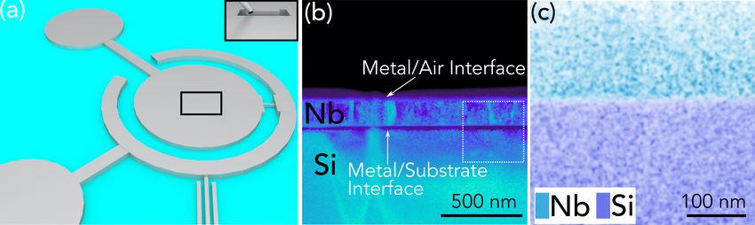
3
sive strain can be attributed to surface stresses present and crystalline substrate [6]. A dark field STEM im-
in this region [16]. Conversely, the tensile stress away age of this surface oxide and the associated thin film
from the interface likely arises from the coalescence is provided in Figure 3a. This image was constructed
of neighboring grains [17]. Meanwhile, the principal by applying a virtual detector with an inner collection
strain along the film growth axis (yy ), the shear strain angle of 10 mrad and an outer collection angle of 15
in the sample plane (xy ) and the rotational strain in mrad, which was designed specifically to match the ini-
the sample plane (τxy ) each exhibit similar profiles. tial diffraction ring observed in the NbOx diffraction
Namely, the largest strains are concentrated near grain pattern (Figure S2). Representative diffraction patterns
boundaries. This is likely due to the pileup of disloca- captured from the indicated regions in the dark field im-
tions in this region to mediate a commensurate atomic age in Figure 3a are provided in Figure 3d-h. The broad
structure between neighboring, but differently oriented diffuse rings we observe are indicative of a lack of long-
grains [18]. This rotational commensurability of adja- range order, which is problematic because it makes this
cent grains may also explain the presence of xy strain oxide prone to hosting TLS defects.
in the film. In all cases, we find that the free surface Since the oxide region exhibits amorphous-like char-
mediates strain relaxation as the strain levels decay to acter in the diffraction pattern, we employ fluctuation
zero in the direction towards the surface. electron microscopy (FEM) to better understand the
Nanometer sized grains with a variety of orientations medium range ordering present in the sample. This
may have implications for qubit performance. One pos- analysis was conducted following the approaches de-
sible mechanism for loss arises because grain boundary tailed previously. [22? –24]. First, this process involves
diffusion is likely the dominant route for solute migra- using a 1 nm probe and capturing diffraction patterns
tion in such systems. With a higher density of grain as a function of position. Following elliptical correction,
boundaries, impurity atoms have more paths to diffuse the radial intensity was then calculated as a function of
from the surface oxide into the Nb film. Other stud- scattering angle. By subtracting the contribution as-
ies have demonstrated that oxygen atoms may prefer- sociated with the thermal motion of atoms as well as
entially segregate along grain boundaries in these sys- the scattering resulting from individual atoms, we were
tems, which may be correlated to reduced T1 times [9]. able to calculate the scattering factor as a function of
Furthermore, because strain fields are found to local- position. Finally upon performing a Fourier transform,
ize at grain boundaries, their associated elastic dipoles the radial distribution function (RDF) as a function of
can lead to interactions between neighboring TLS at the real-space distance is accessible. An RDF profile repre-
grain boundary [10]. These TLS interactions are known sents the probability of finding an atom r distance away
to generate TLS with variable frequencies, which makes from a reference atom. As such, atomic bond distances
device control far more challenging [19]. Moreover, lat- will produce peaks in the profile.
tice strain may induce localized changes in the critical The RDF calculated for positions 1, 3, and 5 in the
temperature and superconducting order parameter[20], dark field image are seen in Figure 3c. From these
and highly strained regions may potentially trap non- profiles, it is apparent that the intensity of the broad
equilibrium quasiparticles. These trapped quasiparti- peak centered about roughly 1.5 Å decreases in inten-
cles have previously been demonstrated to behave sim- sity when moving in the direction away from the surface.
ilarly to other TLS mechanisms in systems exhibiting Based on the calculated radial distribution function pro-
a spatially fluctuating superconducting order parame- file for crystalline Nb2 O5 (Figure S1) [25], this primary
ter, offering another potential source of decoherence in feature is expected to arise from Nb-O bonding. As
this system [21]. Thus, these potential loss mechanisms the experimental RDF is obtained from an amorphous
highlight the importance of manipulating the process- area, disorder arising from local deviations in the bond
ing conditions as well as the underlying substrate to length and bond angles introduce the peak broadening
achieve Nb films with larger grains and improved de- observed compared to the simulated profile. Nonethe-
vice performance. less, we can monitor how this peak evolves throughout
the oxide to obtain information associated with the na-
ture of the Nb-O bonds in this region.
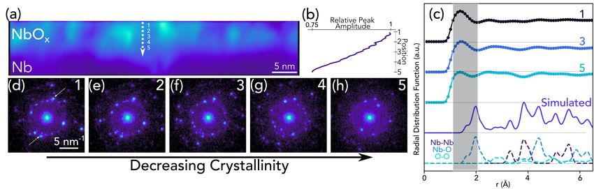
INHOMOGENEITIES IN THE AMORPHOUS Specifically, the peak amplitude of this feature repre-
NIOBIUM SURFACE OXIDE sents the density of Nb-O bonds whereas the peak cen-
ter provides information regarding the bond distances.
In addition to the Nb film, adjacent surfaces and in- As the intensity of this peak corresponding to Nb-O
terfaces are also known to impact the coherence prop- bonds steadily decreases beginning at the top surface
erties in the system. As discussed previously, Nb sur- in the direction towards the Nb film as plotted in Fig-
face oxides, which form spontaneously in ambient condi- ure 3b, this is suggestive of a decrease in the oxygen
tions, exhibit loss tangent values that are roughly three content in this direction. This is in agreement with
orders of magnitude larger than the surrounding film previous findings suggesting that whereas Nb2 O5 has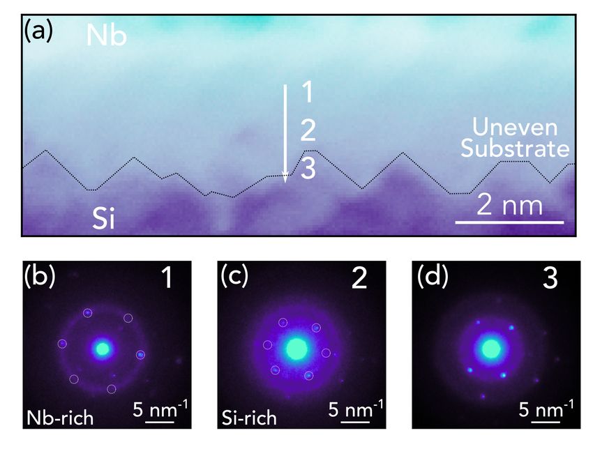
4

Figure 3. Nb/O interface (a) DF image of Nb oxide/Nb constructed using a virtual detector that matched the diffraction
ring of Nb oxide seen in SI Figure 2b. (b) Evolution of normalized primary peak intensity as a function of regions labeled 1-5
in the DF image. (c) Comparison between experimental RDF as a function of position and simulated RDF for crystalline
Nb2 O5 . The intensity of the primary peak at each region was plotted in (b) This simulated profile is also decomposed into
a pair distribution function to understand which pairs of atoms give rise to the features observed. (d-h) Diffraction patterns
taken from regions 1, 2, 3, 4, and 5, respectively. As the distinct diffraction spots indicated by the arrows fade in intensity
from region 1 to region 5, it is apparent that the Nb oxide decreases in crystallinity in the direction away from the surface.

been observed at the surface, NbO2 and NbO are ob-               of position in the direction from the top surface of the
served closer to the Nb film [8, 9, 26]. Based on Figure         NbOx to the Nb film. As such, regions closest to the sur-
3b, it appears that the oxygen concentration evolves             face have a higher likelihood of approaching an ordered
continuously throughout the entire oxide. As the elec-           and stoichiometric Nb2 O5 state. Meanwhile, this mech-
tronic structures of Nb2 O5 differs greatly from NbO2            anism for oxygen transport may cause regions closest to
and NbO, such a concentration gradient implies a spa-            the Nb film to be amorphous and sub-stoichiometric as
tially varying electronic structure that may thus impact         suggested by these findings. Due to the amorphous na-
the resultant superconducting properties of the film.            ture of the sub-oxide, as well as the fact that sub-oxides
   Additionally, the peak position of the Nb-O is plotted        of niobium may give rise to magnetic dipoles,[29] it is
in Figure S1. Based on this peak position map, we ob-            likely that in addition to the large loss tangent value
serve a clear variation in the bond distance throughout          of Nb2 O5 , regions 4 and 5 in Figure 3a play a critical
the oxide. Specifically, we calculate an average bond            role in introducing decoherence in the transmon qubit
distance of 1.39A with a standard deviation of 0.03A.            [30, 31].
This variation in bonding distances throughout the Nb
oxide can lead to tunneling atoms or electrons impos-
ing noise over a wide spectrum as opposed to a single                   NONUNIFORM NIOBIUM/SILICON
frequency [27, 28].                                                             INTERFACE
   In addition to the broad diffuse rings in the electron
diffraction patterns in Figure 3d-h, we also observe a             The metal/substrate interface between Nb and Si
number of distinct diffraction spots. These are espe-            may serve as a source of decoherence as well. In Figure
cially prevalent in the representative diffraction pat-          4a, a phase map of this interface is provided. This map
terns taken from regions 1-3 before appearing to de-             was constructed using virtual annular detectors with
cay in intensity in the representative diffraction pat-          collection angles of 40-45 mrad as well as 20-25 mrad
terns taken from regions 4 and 5. This evolution in the          for Nb and Si, respectively (Figure S3). The former
diffraction pattern is observed throughout the film as           were used to capture signal diffracted from the Nb{110}
highlighted in Figure S2. As the appearance of these             family of planes and the latter were used to capture sig-
distinct diffraction spots is indicative of ordering in the      nal diffracted from the Si{200} family of planes. The
system, this suggests that the Nb oxide closest to the           two resultant maps were overlaid upon one another to
surface (Nb2 O5 ) is more semi-crystalline.                      obtain a qualitative understanding of chemical distri-
   This is reasonable as oxygen diffusion is responsible         bution. Based on the slowly varying intensity gradients
for growth of the surface oxide. In this process, the            in the phase map, we observe that an Nb and Si form
oxygen concentration is expected to decay as a function          an alloy phase that exists between the metal and the
5
T1 coherence times. Because region 3 exhibits signifi-
cant surface roughness and disorder, we expect charge
carriers in these regions to exhibit very low mean free
paths, which may impact the superconductivity prop-
erties.
CONCLUSIONS
In this study, we applied STEM imaging and diffrac-
tion methods to identify structural inhomogeneities and
defects on the atomic and nanoscale in Nb films and as-
sociated interfaces within a test transmon device. Based
on an understanding of loss mechanisms in supercon-
ducting qubits, we hypothesize that many of these fea-
tures may be linked to decoherence. In the Nb film, we
observed grain sizes with the minimum dimension on
Figure 4. Nb/Si interface (a) Phase map of Nb and Si using the order of tens of nanometers and localized strain at
virtual annular detectors shown in Figure S3. (b-d) Diffrac- grain boundary interfaces. In the disordered niobium
tion patterns taken from regions 1, 2, and 3, respectively. surface oxide layer, we observed a significant variation
in the bond distances and in the diffuse metal/substrate
interface, we detected significant atomic disorder and
substrate. Additionally, we also observe that the un- surface roughness. These local structural and atomic
derlying Si substrate is very rough and has likely been features can lead to broad TLS frequency spectra,
altered by the buffered oxide etchant, which is used to charge noise, and impact the superconducting param-
remove Si oxide prior to Nb deposition. eters of the film. As such identification of synthesis
Based on electron diffraction patterns taken across and processing parameters focused on achieving larger
this interface, we define 3 distinct regions that exist be- grains, eliminating the entire surface oxide, and obtain-
tween the crystalline Nb metal and Si substrate. Rep- ing an epitaxial metal/substrate interface offer routes
resentative diffraction patterns taken from each of these to obtaining improved qubit performance.
indicated regions are provided in Figure 4b-d and rep-
resentative diffraction patterns taken from the Nb film
and the Si substrate are provided in Figure S3. Each
of these regions display diffuse rings which are again ACKNOWLEDGEMENTS
indicative of a lack of long-range order. Based on the
presence of intense diffraction spots associated with Nb This material is based upon work supported by the
along with weak diffraction spots associated with Si, we U.S. Department of Energy, Office of Science, National
hypothesize that region 1 is an amorphous niobium sili- Quantum Information Science Research Centers, Su-
cide region that is niobium rich in nature. Conversely perconducting Quantum Materials and Systems Center
through this analysis, region 2 is an amorphous nio- (SQMS) under the contract No. DE-AC02-07CH11359.
bium silicide region that appears to be silicon rich. Fi- This work made use of the EPIC facility of Northwest-
nally, although the diffraction pattern taken from region ern University’s NUANCE Center, which received sup-
3 also exhibits a diffuse ring, the consistency between port from the Soft and Hybrid Nanotechnology Exper-
this diffraction pattern and the reference pattern taken imental (SHyNE) Resource (NSF ECCS-1542205); the
from the Si substrate suggests that this region likely MRSEC program (NSF DMR-1720139) at the Mate-
represents a semi-crystalline region of Si that has been rials Research Center; the International Institute for
roughened during various steps in the deposition and Nanotechnology (IIN); the Keck Foundation; and the
lithography process. State of Illinois, through the IIN. The authors thank
We hypothesize that structural properties in each of members of the Superconducting Quantum Materials
these regions should be investigated and improved for and Systems (SQMS) Center for valuable discussion.
potential coherence benefits. For instance, regions 1 and S. M. R. gratefully acknowledges support from IIN and
2 are amorphous regions, which may house TLS defects. 3M. The authors thank Dr. Anahita Pakzad from Ame-
Additionally, we would expect these niobium silicide re- tek/Gatan, Inc, Pleasanton, CA, for the valuable feed-
gions to be non-superconducting, which would impact back on the usage of the Stela pixelated detector.6
[1] M. Kjaergaard, M. E. Schwartz, J. Braumüller, of Aberration Corrected Electron Microscopy.
P. Krantz, J. I.-J. Wang, S. Gustavsson, and W. D. [16] R. C. Cammarata, Progress in Surface Science 46, 1
Oliver, Annual Review of Condensed Matter Physics (1994).
11, 369 (2020), https://doi.org/10.1146/annurev- [17] C. Wu, Thin Solid Films 64, 103 (1979), international
conmatphys-031119-050605. Conference on Metallurgical Coatings, San Diego, 1979-
[2] G. Wendin, Reports on Progress in Physics 80, 106001 Part III.
(2017). [18] L. R. Nivedita, A. Haubert, A. K. Battu,
[3] N. P. de Leon, K. M. Itoh, D. Kim, K. K. Mehta, and C. V. Ramana, Nanomaterials 10 (2020),
T. E. Northup, H. Paik, B. S. Palmer, N. Samarth, 10.3390/nano10071287.
S. Sangtawesin, and D. W. Steuerman, Science 372 [19] L. Faoro and L. B. Ioffe, Phys. Rev. Lett. 109, 157005
(2021), 10.1126/science.abb2823. (2012).
[4] C. E. Murray, “Material matters in superconducting [20] M. David Henry, S. Wolfley, T. Monson, B. G.
qubits,” (2021), arXiv:2106.05919 [quant-ph]. Clark, E. Shaner, and R. Jarecki, Jour-
[5] A. A. Murthy, J. Lee, C. Kopas, M. J. Reagor, A. P. nal of Applied Physics 115, 083903 (2014),
McFadden, D. P. Pappas, M. Checchin, A. Grassellino, https://doi.org/10.1063/1.4866554.
and A. Romanenko, Applied Physics Letters 120, [21] S. E. de Graaf, L. Faoro, L. B. Ioffe, S. Ma-
044002 (2022), https://doi.org/10.1063/5.0079321. hashabde, J. J. Burnett, T. Lindström, S. E.
[6] A. Romanenko, R. Pilipenko, S. Zorzetti, D. Frolov, Kubatkin, A. V. Danilov, and A. Y. Tza-
M. Awida, S. Belomestnykh, S. Posen, and A. Gras- lenchuk, Science Advances 6, eabc5055 (2020),
sellino, Phys. Rev. Applied 13, 034032 (2020). https://www.science.org/doi/pdf/10.1126/sciadv.abc5055.
[7] C. R. H. McRae, H. Wang, J. Gao, M. R. Vissers, [22] E. Kennedy, N. Reynolds, L. Rangel DaCosta,
T. Brecht, A. Dunsworth, D. P. Pappas, and J. Mu- F. Hellman, C. Ophus, and M. C. Scott,
tus, Review of Scientific Instruments 91, 091101 (2020), Applied Physics Letters 117, 091903 (2020),
https://doi.org/10.1063/5.0017378. https://doi.org/10.1063/5.0015532.
[8] J. Verjauw, A. Potočnik, M. Mongillo, R. Acharya, [23] T. F. Harrelson, E. Sheridan, E. Kennedy, J. Vin-
F. Mohiyaddin, G. Simion, A. Pacco, T. Ivanov, son, A. T. N’Diaye, M. V. P. Altoé, A. Schwartzberg,
D. Wan, A. Vanleenhove, L. Souriau, J. Jussot, I. Siddiqi, D. F. Ogletree, M. C. Scott, and S. M.
A. Thiam, J. Swerts, X. Piao, S. Couet, M. Heyns, Griffin, Applied Physics Letters 119, 244004 (2021),
B. Govoreanu, and I. Radu, Phys. Rev. Applied 16, https://doi.org/10.1063/5.0069549.
014018 (2021). [24] X. Mu, D. Wang, T. Feng, and C. Kübel, Ultrami-
[9] A. Premkumar, C. Weiland, S. Hwang, B. Jaeck, croscopy 168, 1 (2016).
A. P. M. Place, I. Waluyo, A. Hunt, V. Bisogni, J. Pel- [25] C. L. Farrow, P. Juhas, J. W. Liu, D. Bryndin, E. S.
liciari, A. Barbour, M. S. Miller, P. Russo, F. Camino, Božin, J. Bloch, T. Proffen, and S. J. L. Billinge, Jour-
K. Kisslinger, X. Tong, M. S. Hybertsen, A. A. Houck, nal of Physics: Condensed Matter 19, 335219 (2007).
and I. Jarrige, arXiv (2020), 2004.02908 [physics.app- [26] I. Lindau and W. E. Spicer, Journal of Applied Physics
ph]. 45, 3720 (1974), https://doi.org/10.1063/1.1663849.
[10] C. Müller, J. H. Cole, and J. Lisenfeld, Reports on [27] J. M. Martinis, K. B. Cooper, R. McDermott, M. Stef-
Progress in Physics 82, 124501 (2019). fen, M. Ansmann, K. D. Osborn, K. Cicak, S. Oh, D. P.
[11] C. Ophus, Microscopy and Microanalysis 25, 563–582 Pappas, R. W. Simmonds, and C. C. Yu, Phys. Rev.
(2019). Lett. 95, 210503 (2005).
[12] S. M. Ribet, A. A. Murthy, E. W. Roth, R. dos [28] A. P. Paz, I. V. Lebedeva, I. V. Tokatly, and A. Rubio,
Reis, and V. P. Dravid, Materials Today (2021), Phys. Rev. B 90, 224202 (2014).
https://doi.org/10.1016/j.mattod.2021.05.006. [29] E. Sheridan, T. F. Harrelson, E. Sivonxay, K. A. Pers-
[13] A. Nersisyan, S. Poletto, N. Alidoust, R. Manenti, son, M. V. P. Altoé, I. Siddiqi, D. F. Ogletree, D. I. San-
R. Renzas, C.-V. Bui, K. Vu, T. Whyland, Y. Mohan, tiago, and S. M. Griffin, “Microscopic theory of mag-
E. A. Sete, S. Stanwyck, A. Bestwick, and M. Reagor, netic disorder-induced decoherence in superconducting
in 2019 IEEE International Electron Devices Meeting nb films,” (2021), arXiv:2111.11684 [cond-mat.supr-
(IEDM) (2019) pp. 31.1.1–31.1.4. con].
[14] M. R. Vissers, J. Gao, D. S. Wisbey, D. A. Hite, [30] A. Sundaresan, R. Bhargavi, N. Rangarajan, U. Sid-
C. C. Tsuei, A. D. Corcoles, M. Steffen, and D. P. desh, and C. N. R. Rao, Phys. Rev. B 74, 161306(R)
Pappas, Applied Physics Letters 97, 232509 (2010), (2006).
https://doi.org/10.1063/1.3517252. [31] R. J. Cava, B. Batlogg, J. J. Krajewski, H. F. Poulsen,
[15] T. C. Pekin, C. Gammer, J. Ciston, A. M. Minor, and P. Gammel, W. F. Peck, and L. W. Rupp, Phys. Rev.
C. Ophus, Ultramicroscopy 176, 170 (2017), 70th Birth- B 44, 6973 (1991).
day of Robert Sinclair and 65th Birthday of Nestor J.
Zaluzec PICO 2017 – Fourth Conference on FrontiersYou can also read