Single-Grain Gate-All-Around Si Nanowire FET Using Low-Thermal-Budget Processes for Monolithic Three-Dimensional Integrated Circuits - MDPI
←
→
Page content transcription
If your browser does not render page correctly, please read the page content below
micromachines

Article
Single-Grain Gate-All-Around Si Nanowire FET
Using Low-Thermal-Budget Processes for Monolithic
Three-Dimensional Integrated Circuits
Tung-Ying Hsieh 1,2 , Ping-Yi Hsieh 3 , Chih-Chao Yang 3, *, Chang-Hong Shen 3 , Jia-Min Shieh 3 ,
Wen-Kuan Yeh 3 and Meng-Chyi Wu 1
 1   Institute of Electronics Engineering, National Tsing Hua University, Hsinchu 30013, Taiwan;
     tyhsieh@narlabs.org.tw (T.-Y.H.); mcwu@ee.nthu.edu.tw (M.-C.W.)
 2   National Applied Research Laboratories, 3F, No. 106, Ho Ping E. Rd., Sec. 2, Taipei City 10622, Taiwan
 3   Taiwan Semiconductor Research Institute, No.26, Prosperity Road 1, Hsinchu 30013, Taiwan;
     1805047@narlabs.org.tw (P.-Y.H.); chshen@narlabs.org.tw (C.-H.S.); jmshieh@narlabs.org.tw (J.-M.S.);
     1305023@narlabs.org.tw (W.-K.Y.)
 *   Correspondence: samyang@narlabs.org.tw; Tel.: +886-3-5276110 (ext. 7565)

 Received: 4 July 2020; Accepted: 30 July 2020; Published: 30 July 2020

 Abstract: We introduce a single-grain gate-all-around (GAA) Si nanowire (NW) FET using the location-
 controlled-grain technique and several innovative low-thermal budget processes, including green
 nanosecond laser crystallization, far-infrared laser annealing, and hybrid laser-assisted salicidation, that keep
 the substrate temperature (Tsub) lower than 400 ◦C for monolithic three-dimensional integrated circuits
 (3D-ICs). The detailed process verification of a low-defect GAA nanowire and electrical characteristics
 were investigated in this article. The GAA Si NW FETs, which were intentionally fabricated within the
 controlled Si grain, exhibit a steeper subthreshold swing (S.S.) of about 65 mV/dec., higher driving currents
 of 327 µA/µm (n-type) and 297 µA/µm (p-type) @ Vth ± 0.8 V, and higher Ion/Ioff (>105 @|Vd| = 1 V)
 and have a narrower electrical property distribution. In addition, the proposed Si NW FETs with a
 GAA structure were found to be less sensitive to Vth roll-off and S.S. degradation compared to the
 omega(Ω)-gate Si FETs. It enables ultrahigh-density sequentially stackable integrated circuits with
 superior performance and low power consumption for future mobile and neuromorphic applications.

 Keywords: monolithic 3D; gate-all-around; nanowire FET; low-thermal budget; location-controlled-
 grain; laser crystallization; laser activation; laser-assisted salicidation; low power consumption

1. Introduction
     To catch up to Moore’s law, and to benefit from a faster computing speed and economical chip,
there are two approaches [1,2] followed and adopted in the semiconductor industry: one is “more
Moore” which means keep downsizing the dimension of the transistor using a new device structure or
non-silicon materials; the other is “more than Moore” which introduces a heterogeneous integration
concept in the out-of-plane direction. The latter is also known as three-dimensional integrated circuits
(3D-ICs). Although through silicon via (TSV) technology [3] is the dominating process in modern 3D-ICs,
monolithic 3D-ICs [4,5] have drawn increasing attention in recent years which can offer additional
transistor layers using either front end of line (FEOL) or back end of line (BEOL) processes for integrated
circuits, and thereby provide several advantages, such as the reduction of latency, flexibility, high
connectivity, and low power consumption [6].
     Low-temperature polycrystalline-silicon (LTPS) thin-film transistors (TFTs) fabricated by excimer
laser crystallization (ELC) drew tremendous attention in the 1980s [7,8] for their great potential in
realizing three-dimensional integrated circuits (3D-ICs). However, the random grain size distribution,

Micromachines 2020, 11, 741; doi:10.3390/mi11080741                          www.mdpi.com/journal/micromachines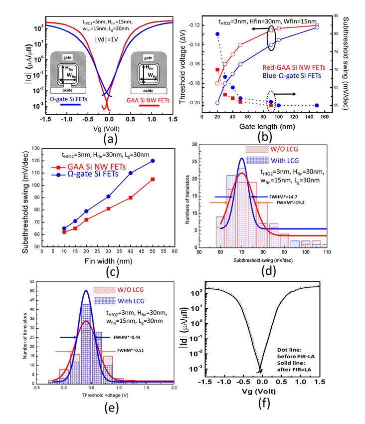
Micromachines 2020, 11, 741                                                                           2 of 12

the unpredictable grain boundary, and the narrow process window to prevent damages on the bottom tier
become ineluctable issues [9,10]. To date, there has been several researches aiming to develop sequentially
3D stackable techniques using a layer transfer method, namely SmartCutTM with semiconductor-
on-insulator wafers, e.g., SOI, GOI, or III-V-OI [11,12]. Although this technique could provide better
channel quality, it still needs to face the potential high-temperature annealing process of 3D stackable
transistor manufacturing. In addition, the process complexity and costly investment may hinder its
widespread development. In contrast, there are several groups trying to modify the recrystallization
process to prevent the grain boundary effect and to minimize the number of grain boundaries within the
active region of a device. One of them is the µ-Czochralski process that tries to control the grain location
so then devices can be manufactured within the grain [13–15]. However, the thick and rough channel is
not appropriate for modern nano-electronics. The main task is to develop a thin and high-crystallinity
channel and further low-thermal budget processes for sequentially 3D stackable devices with high
performance and low variability.
     In this article, we adopted a µ-Czochralski process using pulse laser crystallization followed by a
chemical mechanical polish (CMP) and surface modification steps to fabricate a thin and high-crystallinity
location-controlled grain (LCG) Si nanowire channel for its high positioning accuracy, predictability,
and compatibility with our present process. A gate-all-around configuration to detach the Si and buried
SiO2 for a nano-scale transistor, which is much smaller than the grain size of the Si channel, integrated
with several innovative low-thermal budget processes was demonstrated. The single-grain GAA Si NW
FETs and processes earn not only high performance and low variability but the extremely scaled NW
dimension, which, in turn, enables the application for advanced monolithic 3D-ICs.

2. Materials and Methods
      The process flow of the monolithic 3D single-grain gate-all-around Si nanowire FET is depicted
in Figure 1. The key of fabricating such a sequentially 3D stackable transistor or further integrated
circuit lies in developing low-thermal budget processes, which means the substrate temperature should
not be higher than 400 ◦ C to keep the metal interconnect reliable and to be compatible with BEOL
processes [16,17]. To prepare a high-crystallinity and LCG Si channel, we use a shaped e-beam direct
write lithography system and inductively coupled plasma (ICP) etching to create periodic cooling
holes on buried oxide as a grain filter before deposing a conformal and 150-nm-thick amorphous Si
(a-Si) film. Afterwards, the a-Si film was recrystallized and phase-transformed to a location-controlled
and large-grain polycrystalline Si film by Nd:YAG diode-pumped solid-state (DPSS) continuous wave
green nanosecond laser annealing (GNS-LA) (Figure 1a). The wavelength, pulse width, scanning
speed, beam size, and power of the laser are λ = 532 nm, 13 ns, 25 cm/s, 2 mm × 40 µm, and 5.5 W,
respectively. To remove the surface defects caused by the laser process and to improve the overall
channel uniformity, the CMP was introduced to thin the thick and large-grain polycrystalline Si film
down to below 50 nm (Figure 1b). Afterward, an NW was preliminary defined by a shaped e-beam
direct write lithography system and the ICP etching process.
      A whole chemical process was then proceeded to suspend NW in this article as follows: a. soak
into two mixture solutions (NH4 OH:H2 O2 :H2 O = 1:4:20 and HCl:H2 O2 :H2 O = 1:1:6) at 75 ◦ C for 10 min
to remove polymer residues and particles caused by the photoresist stripping process (Figure 1c);
b. immerse into pure H2 O2 as a strong oxidizing agent for 3 minutes at 100◦ C to grow sacrificial oxide
on the Si surface (Figure 1d); c. suspend the Si NW by removing the sacrificial oxide using dilute HF
solution (HF:H2 O = 1:10) for 5 min (Figure 1e).
      The gate stack was fabricated by 3nm-thick HfO2 and 50-nm-thick TaN metal layers using atomic
layer deposition (ALD) for its excellent step coverage and self-limiting nature around the NW as high-K
gate dielectric and metal electrode (HK/MG), respectively (Figure 1f). The gate length of the Si NW FET
was defined by shaped e-beam direct write lithography ICP etching process. The exposed channel region
was then doped with P31+ or BF2 49+ at a dosage of 5 × 1015 cm−2 (10 KeV) for N-type or P-type MOSFETs
through self-aligned ion implantation and was activated by a CO2 FIR-LA to form a highly-activated,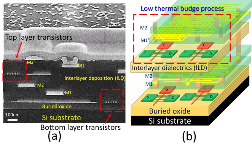
Micromachines 2020, 11, 741 3 of 12
abrupt, and ultra-shallow junction source and drain regions (Figure 1g). The wavelength, power,
and substrate2020,
temperature of FIR-LA ◦
Micromachines 11, x FOR PEER REVIEWwere 10.6 µm, 125 W, and 350 C, respectively. 3 of 13
2
Figure 1. Schematics of process steps for 3D stackable single-grain gate-all-around (GAA) Si nanowire
Figure
(NW) 1. Schematics
FET: (a) a-Si film ofwas
process steps for by
crystallized 3D GNS-LA;
stackable single-grain
(b) the chemicalgate-all-around
mechanical(GAA) Si nanowire
polishing (CMP);
(c) NW with defects was preliminary defined by lithography and ICP etching process in a Si(CMP);
(NW) FET: (a) a-Si film was crystallized by GNS-LA; (b) the chemical mechanical polishing gain;
(c)soak
(d) NW into
withtwo
defects was solutions
mixture preliminary defined polymer
to remove by lithography
residuesandandICP etchingand
particles process in a Si
immerse gain;
into (d)
pure
Hsoak
O
2 2 into
to formtwo mixture
sacrificial solutions
oxide on to
the remove
Si NW polymer
surface; (e) residues
suspend and
the particles
Si NW by and immerse
removing the into pure
sacrificial
H2O2using
oxide to form sacrificial
dilute oxide (f)
HF solution; on high-K/metal
the Si NW surface; (e) suspend
gate (HK/MG) stackthe Si NW by
fabricated byremoving the sacrificial
ALD; (g) implantation
oxide using dilute HF solution; (f) high-K/metal gate (HK/MG) stack fabricated
and far-infrared laser annealing (FIR-LA) for dopant activation, (h) hybrid laser-assisted self-aligned by ALD; (g)
implantation
silicide and (i) and far-infrared
interlayer laserlayer
dielectric annealing (FIR-LA) for
(ILD) deposition dopant
and activation,
following (h) hybrid
standard laser-assisted
metallization using
self-aligned
tungsten silicide and (i) interlayer dielectric layer (ILD) deposition and following standard
(W) interconnect.
metallization using tungsten (W) interconnect.
Moreover, a two-step hybrid laser-assisted self-aligned silicide (Salicide) was also adopted to
replace Athe conventional
whole chemical high-temperature
process was then Salicide
proceeded process [18,19].NW
to suspend In thein process, a 10-nm-thin
this article as follows:Ni a. film
soak
was
intosputtered
two mixtureon the NW surface
solutions (NH4OH:Hafter 2SiN
O2:H x 2spacer formation.
O = 1:4:20 and HCl:H The2Ofirst-step annealing
2:H2O = 1:1:6) was
at 75 °C forcarried
10 min
out at 250 ◦ Cpolymer
to remove for 30 s residues
in a rapidandthermal annealing
particles caused(RTA)
by thesystem to form
photoresist a high-resistivity
stripping Ni2 Si phase.
process (Figure 1c); b.
After removing the unreacted Ni by soaking into a 1:10 HNO solution at 50 ◦ C for 600 s, the second-step
immerse into pure H2O2 as a strong oxidizing agent for 33minutes at 100°C to grow sacrificial oxide
annealing
on the Si was followed
surface (Figureby1d);
a CO FIR-LA with
c.2suspend the Si100W
NW laser power atthe
by removing room temperature
sacrificial oxidetousing
transform
dilutethe HF
Ni 2 Si
solutionphase into
(HF:H 2aO low-resistivity
= 1:10) for 5 minNiSi phase
(Figure (Figure
1e). 1h).
After performing
The gate stack was allfabricated
the low-thermal budgetHfO
by 3nm-thick processes to fabricateTaN
2 and 50-nm-thick the single-grain
metal layersGAAusingSi NW
atomic
FETs,
layer SiO 2 deposition
deposition (ALD) as for
an its
interlayer
excellentdielectric layer (ILD)
step coverage followed by nature
and self-limiting a standard
aroundmetallization
the NW as
process
high-K using tungstenand
gate dielectric (W)metal
metalelectrode
were then proceeded
(HK/MG), to accomplish
respectively (Figurethe1f).
first
Thestacked deviceoftier
gate length the
(Figure
Si NW 1i).FETAwastwo-tier
definedmonolithic
by shaped3D-IC
e-beamcandirect
be simply
write realized
lithographyby repeating
ICP etching theprocess.
whole low-thermal
The exposed
budget
channel process
region(T was < 400doped
sub then
◦ C) (Figure 2a,b).
with P31+ or BF2 49+ at a dosage of 5 × 1015 cm−2 (10 KeV) for N-type or
P-type MOSFETs through self-aligned ion implantation and was activated by a CO2 FIR-LA to form
a highly-activated, abrupt, and ultra-shallow junction source and drain regions (Figure 1g). The
wavelength, power, and substrate temperature of FIR-LA were 10.6 µm, 125 W, and 350 °C,
respectively.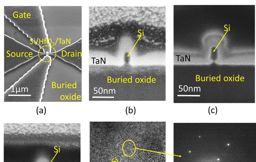
s, the second-step annealing was followed by a CO2 FIR-LA with 100W laser power at room
temperature to transform the Ni2Si phase into a low-resistivity NiSi phase (Figure 1h).
After performing all the low-thermal budget processes to fabricate the single-grain GAA Si NW
FETs, SiO2 deposition as an interlayer dielectric layer (ILD) followed by a standard metallization
process using tungsten (W) metal were then proceeded to accomplish the first stacked device tier
Micromachines 1i). A11,
(Figure 2020, 741
two-tier monolithic 3D-IC can be simply realized by repeating the whole low-thermal 4 of 12
budget process (Tsub < 400 °C) (Figure 2a,b).
Figure 2. (a) SEM image of a 3D sequential integration with two stacking tiers and each tier has a
FigureW
two-layer 2. interconnect
(a) SEM image(M1-M2).
of a 3D sequential integration
(b) Schematic with two
illusion of a stacking
monolith tiers and each tier has aintegrated
three-dimensional two-
layer W interconnect (M1-M2). (b) Schematic illusion of a monolith three-dimensional integrated
circuit (3DIC) using single-grain GAA Si NW FETs.
circuit (3DIC) using single-grain GAA Si NW FETs.
3. Results and Discussion
3. Results and Discussion
3.1. High-Crystallinity and Controlled-Grain Si Film
3.1. High-Crystallinity and Controlled-Grain Si Film
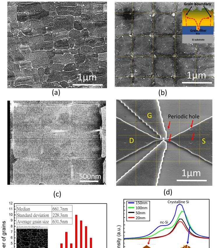
Figure 3a depicts an SEM image of a random grain growth Si channel on the buried oxide after
Figure 3a depicts an SEM image of a random grain growth Si channel on the buried oxide after
GNS-LA. Apparently, without any specific structure of the surface or crystallization method, the grain
GNS-LA. Apparently, without any specific structure of the surface or crystallization method, the
size and
graingrain boundary
size and were randomly
grain boundary distributed.
were randomly The The
distributed. grain boundary
grain boundaryin in
the
theSiSichannel
channel may
may have
unreacted dangling bonds
have unreacted dangling or hydrogen-passivated –Si-H bonds
bonds or hydrogen-passivated –Si-Hthat decrease
bonds the carrier
that decrease themobility
carrier and
degrade the device
mobility performance
and degrade [20–22].
the device In contrast,
performance Figure
[20–22]. 3b shows
In contrast, an SEM
Figure image
3b shows anof a Siimage
SEM channel
of with
a regular Si matrix
a Si channel using
with the location-controlled-grain
a regular technique, as illustrated
Si matrix using the location-controlled-grain in the
technique, as inset. The in
illustrated cooling
hole the
actsinset. The cooling
as a grain filter forhole actsgrain
lateral as a growth
grain filter for lateral
during grain and
the melted growth duringlaser
quenched the melted and
recrystallization
quenched laser recrystallization process. The grain boundaries appeared while the neighbor
process. The grain boundaries appeared while the neighbor grains were met together. This can be clearly grains
were met together. This can be clearly observed after CMP and SEECO etch as shown in Figure 3c.
observed after CMP and SEECO etch as shown in Figure 3c. The GAA Si NW FET was designed and
The GAA Si NW FET was designed and intentionally located within a single grain to avoid
intentionally located within a single grain to avoid overlapping the grain boundaries (Figure 3d) which
overlapping the grain boundaries (Figure 3d) which can guarantee better device performance and
can guarantee better device performance and less output characteristic variation for the monolithic
less output characteristic variation for the monolithic 3DIC design [23,24].
3DIC design [23,24].
Moreover, a quantitative grain size distribution analysis was conducted by the ImageJ software
(Figure 3e). Compared to an approximate grain size around 900 nm extracted from the location-controlled-
grain Si film, the Si channel without periodic cooling holes exhibits a broad grain size distribution with
a standard deviation of 228.3 nm and an average grain size of 631.5 nm from the statistical data in the
Figure 3e. The smallest grain size was only about 100 nm that was slightly larger than the size of the
GAA Si NW FET. This raises the probability of nano-devices located on the grain boundary. This result
suggests that the introduction of periodic cooling holes on buried oxide before the laser crystallization
process can effectively achieve a location-controlled-grain Si film.
In addition to the µ-Czochralski process, the CMP process was also adopted for fabricating a
thin and uniform Si channel after the short-pulse GNS-LA. As a result, the CMP not only eliminates
the surface roughness but also removes defect and nanocrystalline Si phase layer on the uneven
channel surface. Figure 3f shows the AFM images and Raman spectroscopy. The surface roughness of
the Si channel dropped from 14.6 to 1.17 nm and the crystallinity was improved while the channel
thickness was decreased from 150 to 20 nm. Evidentially, a Raman peak at 520 cm−1 representing a
nanocrystalline Si signal vanished after the CMP process, revealing the poor crystallinity on the surface
due to the slower cooling rate in the interfacial region [25].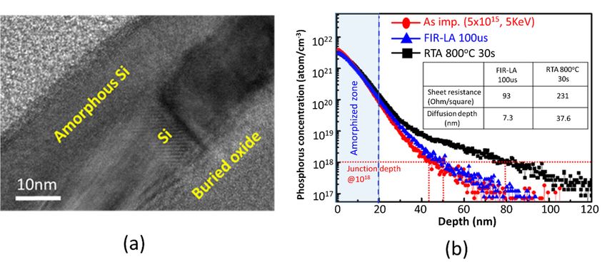
Micromachines 2020, 11, 741                                                                                     5 of 12
 Micromachines 2020, 11, x FOR PEER REVIEW                                                                     5 of 13

      Figure 3. (a) SEM image of random grain growth poly-Si channel; (b) SEM image of a Si matrix using the
        Figure 3. (a) SEM image of random grain growth poly-Si channel; (b) SEM image of a Si matrix using
      LCG technique with the grain filter illustrated in the inset; (c) SEM image of a thin LCG Si film after CMP
        the LCG technique with the grain filter illustrated in the inset; (c) SEM image of a thin LCG Si film
      and SEECO etch (solution of K2 Cr2 O7 water mixed with HF) to reveal the grain boundaries; (d) SEM
        after CMP and SEECO etch (solution of K2Cr2O7 water mixed with HF) to reveal the grain boundaries;
      image of a single grain GAA Si NW FET intentionally located in a Si gain; (e) grain size distribution of
        (d) SEM image of a single grain GAA Si NW FET intentionally located in a Si gain; (e) grain size
      a Si channel without the LCG technique and the inset is the image analysis conducted by the ImageJ
        distribution of a Si channel without the LCG technique and the inset is the image analysis conducted
      software. (f) The Raman spectrums of the Si channel before and after the CMP thinning process and
        by the ImageJ software. (f) The Raman spectrums of the Si channel before and after the CMP thinning
      inset AFM images show the related surface morphology and the root mean square roughness.
        process and inset AFM images show the related surface morphology and the root mean square
        roughness.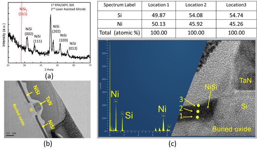
Micromachines 2020, 11, 741                                                                                              6 of 12

3.2. Gate-All-Around Si Nanowire FET Fabrication
      Ultra-thin-body (UTB) silicon in an insulator (SOI) configuration has been widely studied and
adopted in our previous works [26–29] for its outstanding electrostatics due to excellent suppression of
the short channel effects (SCEs). However, it is still hard to thoroughly remove the interface traps and
fixed oxide defects in back oxide which inevitably degrade the device performance [30,31]. For the
recrystallized poly-Si channel, this issue becomes more serious, because the fast quench speed causes
more interface defects between the poly-Si and buried oxide interface. Here, a configuration evolution
from UTB to GAA was achieved by proposing a whole chemical process to suspend the single-grain Si
NW and to eliminate the interface traps and fixed oxide defects.
      By precisely controlling the soaking time of dilute HF that consumes sacrificial oxide and buried
oxide, we can simply obtain a single-grain GAA Si NW FET. Figure 4a shows a tilted SEM image of
a single-grain GAA Si NW FET with a multi-nanowire channel in order to increase the total driving
current. The active region of the FET was intentionally designed and fabricated within a single Si grain.
The number of nanowires depends on the grain size and the limitation of the lithographic process.
For example, we may put an 8 × 4 static random-access memory (SRAM) mini-array within a grain
with a size of 1.04 × 0.83 µm following the 7-nm-node IC design rule [32,33]. For the transistor beyond
Micromachines
a 5-nm-node,  2020,
                 we 11,may
                        x FOR PEER
                            put    REVIEW
                                more  FETs or even functional units within a Si grain.             7 of 13

      Figure 4. (a) A tilted SEM image of a multi-wire GAA Si NW FET. The configurations of (b) tri-gate,
     Figure  4. (a)and
      (c) Ω-gate,   A tilted SEM
                       (d) GAA   Si image of different
                                    FET with a multi-wire   GAA
                                                       soaking    Si NW
                                                                times       FET.
                                                                       in the    The configurations
                                                                              channel  fabrication step.of(e)
                                                                                                           (b)Atri-gate,
                                                                                                                HRTEM
     (c) Ω-gate,
      image        and (d) GAA
             of single-grain       Si FET
                              Si and  HfO2with  different
                                           dialectic layer.soaking   times area
                                                            (f) A selected   in the  channel pattern
                                                                                  diffraction fabrication
                                                                                                      (SADP)step.from
                                                                                                                   (e) A
                                                                                                                       Si.
     HRTEM image of single-grain Si and HfO2 dialectic layer. (f) A selected area diffraction pattern
     (SADP) from Si.

3.3. Highly Activated Ultra-Shallow-Junction Formed by FIR-LA
    One of the bottle-necks in monolithic 3D GAA Si NW FET devices is to form highly activated
(low sheet resistance Rsh) source/drain extensions with abrupt, ultra-shallow junctions (USJ) [34,35].
How to repair the amorphized surface bombarded by dopant species as well as to avoid severe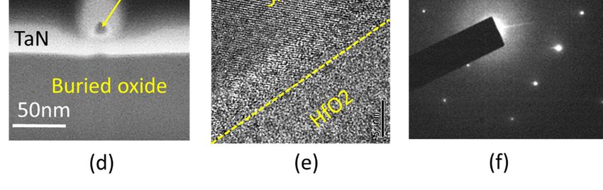
Micromachines 2020, 11, 741                                                                             7 of 12

      A progressive evolution of device configuration fabricated by increasing HF soaking time is
exhibited in Figure 4b–d. An Ω-gate Si FET was demonstrated while the buried oxide underneath was
partially etched away, as shown in Figure 4c. The coverage of the HK/MG stack can be increased to
enhance controllability by a longer soaking time to totally detach the buried oxide that touches the Si
channel. The ultimate GAA Si NW FET with Wfin /Hfin /Lgate = 15 nm/15 nm/30 nm was achieved by 5
min soaking time as presented in Figure 4d. The high-resolution transmission electron microscopy
(HRTEM) image in Figure 4e exhibits an ALD-deposited HfO2 and a single-grain Si lattice. The selected
area diffraction pattern (SADP) for the laser-crystallized channel in Figure 4f reveals that the Si channel
is highly recrystallized.

3.3. Highly Activated Ultra-Shallow-Junction Formed by FIR-LA
     One of the bottle-necks in monolithic 3D GAA Si NW FET devices is to form highly activated
(low sheet resistance Rsh ) source/drain extensions with abrupt, ultra-shallow junctions (USJ) [34,35].
How to repair the amorphized surface bombarded by dopant species as well as to avoid severe dopant
diffusion that causes the SCEs during the high-energy activation and heat dissipation through the ILD
downward to the bottom metal interconnect and device/circuits become a key challenge.
     The introduced FIR-LA is an intraband excitation process [36,37]. It can selectively transfer energies
to the free carriers and repairs defects or activates the dopants without damaging the top HK/MG
nano-structure of a gate-first device. The limited heating zone and short process duration result in fast
heat dissipation and therefore keep the bottom metal interconnects and the device/circuit “cool”.
     A high-resolution transmission electron microscope (HRTEM) image of a Si after the dopant
implantation process is shown in Figure 5a and clearly indicates that the surface is bombarded into
disorder. The amorphous Si layer is about 15-nm-thin, appearing after the P31+ dopant implantation at
a heavy dosage of 5 × 1015 cm−2 and 5 KeV ion energy. With an FIR-LA condition of 125 W laser power
for 100 µs at 350 ◦ C annealing temperature, the amorphous layer shall be epitaxial regrown. Figure 5b
shows the dopant profiles with and without the FIR-LA using a secondary ion mass spectrometer
(SIMS) and they are compared to conventional rapid thermal annealing (RTA). Apparently, a 37.6 nm
diffusion depth at the level of 1018 dopant concentration was observed in conventional RTA at 800 ◦ C
for 10 s annealing time which increases the risk of current leakage between source and drain due to
lateral diffusion in the nanodevices. In contrast, the FIR-LA contributes only a 7.3 nm diffusion depth
which reflects the fact that a short-pulse and long-wavelength laser annealing effectively suppresses
the SCEs. The series resistance in the inset table, which is another index of the annealing process and
dominates the final performance of a scaling device, was further reduced from 213 to 93 Ohm/γ by
adopting the FIR-LA to replace conventional RTA. The nearly diffusionless dopant profiles and low
resistivity represent the advantage of such a low-thermal budget FIR-LA in monolithic 3D-ICs.

3.4. Hybrid Laser-Assisted Salicidation
      Nickel salicidation is a crucial process for advanced MOS transistors for its low Si consumption,
low formation temperature, and low line width sheet resistance dependence as compared to cobalt or
titanium silicide [18,19]. Previous studies proved that a rough NiSi film and NiSi2 facet (111) formed
during conventional two-step RTA, which will lead to Fermi-level pining and a junction spiking
leakage current [38,39]. Additionally, the second step of conventional two-step RTA usually reaches
400 to 600 ◦ C to form a low-resistivity NiSi film, which is slightly higher than the BEOL CMOS process
requirement that may cause a reliability issue for monolithic stacking [9,10]. Here, we introduce a
hybrid laser-assisted salicidation process, that is first annealed at 250 ◦ C for 30 s in an RTA system
followed by second-step FIR-LA with 100 µs process time at room temperature (Tsub = 25 ◦ C), to form
a thin and uniform Si-rich NiSix film as well as to suppress the formation of NiSi2 facet (111).
      The X-ray diffraction (XRD) patterns of nickel silicide formed by the hybrid laser-assisted salicidation
process were displayed in Figure 6a. Five nickel monosilicide (NiSi) peaks, corresponding to the (0 0 2),
(1 1 1), (2 0 2), (1 0 3), and (0 1 3) lattice planes, were observed and no NiSi2 facet (1 1 1) was found,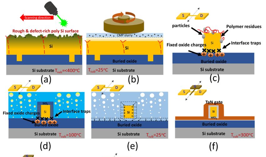
Micromachines 2020, 11, 741 8 of 12
Micromachines 2020, 11, x FOR PEER REVIEW 8 of 13
which promises aRTA
conventional high-quality
at 800 °Candforlow-resistivity
10 s annealingNiSi timefilm. The increases
which morphologythe of theofNiSi
risk film prepared
current leakage
by between
the hybrid laser-assisted salicidation process was analyzed by high-resolution transmission
source and drain due to lateral diffusion in the nanodevices. In contrast, the FIR-LA electron
microscopy
contributes(HRTEM).
only a 7.3Thenmsecond-step
diffusion FIR-LA melts the
depth which high-resistivity
reflects Ni2aSishort-pulse
the fact that phase near and the surface
long-
andwavelength
the melt front
laserdiffuses
annealingdownward to the
effectively Si and Ni
suppresses the
2 Si interface.
SCEs. The The
seriesmixing of
resistance Niin2 Si
the and Si
inset occurs
table,
viawhich
liquid is another
phase index [38],
diffusion of the annealing
which leads process and dominates
to a uniform the finalheterogeneous
NiSi film without performance of a scaling
aggregation
anddevice,
spike was further
at the reduced
interface fromthe
between 213NiSi
to 93 Ohm/γ
and bywhich
the Si, adopting the FIR-LA
is confirmed in to replace
Figure 6b,c.conventional
The atomic
RTA. Theofnearly
percentage diffusionless
Si, identified dopant profiles and
by energy-dispersive lowspectroscopy
X-ray resistivity represent the advantage
(EDS), slightly raises fromof such a
49.87
low-thermal budget FIR-LA in monolithic 3D-ICs.
(point 1) to 54.74% (point 3), implying Ni2 Si diffused from the surface to the bottom.
Figure 5. (a) A HRTEM image of Si after dopant implantation. (b) Dopant profiles characterized by
Figure 5. (a) A HRTEM image of Si after dopant implantation. (b) Dopant profiles characterized by a
a secondary ion mass spectrometer (SIMS). The inset table presents the sheet resistance differences
secondary ion mass spectrometer (SIMS). The inset table presents the sheet resistance differences
between FIR-LA
Micromachines 2020, 11, xand
FORRTA. REVIEW
between FIR-LA andPEER
RTA. 9 of 13
3.4. Hybrid Laser-Assisted Salicidation
Nickel salicidation is a crucial process for advanced MOS transistors for its low Si consumption,
low formation temperature, and low line width sheet resistance dependence as compared to cobalt
or titanium silicide [18,19]. Previous studies proved that a rough NiSi film and NiSi2 facet (111)
formed during conventional two-step RTA, which will lead to Fermi-level pining and a junction
spiking leakage current [38,39]. Additionally, the second step of conventional two-step RTA usually
reaches 400 to 600 °C to form a low-resistivity NiSi film, which is slightly higher than the BEOL CMOS
process requirement that may cause a reliability issue for monolithic stacking [9,10]. Here, we
introduce a hybrid laser-assisted salicidation process, that is first annealed at 250 °C for 30 s in an
RTA system followed by second-step FIR-LA with 100 µs process time at room temperature (Tsub = 25
°C), to form a thin and uniform Si-rich NiSix film as well as to suppress the formation of NiSi2 facet
(111).
The X-ray diffraction (XRD) patterns of nickel silicide formed by the hybrid laser-assisted
salicidation process were displayed in Figure 6a. Five nickel monosilicide (NiSi) peaks,
corresponding to the (0 0 2), (1 1 1), (2 0 2), (1 0 3), and (0 1 3) lattice planes, were observed and no
NiSi2 facet (1 1 1) was found, which promises a high-quality and low-resistivity NiSi film. The
morphology of the NiSi film prepared by the hybrid laser-assisted salicidation process was analyzed
byFigure 6. (a) The XRD
high-resolution patterns of theelectron
transmission nickel silicide formed by(HRTEM).
microscopy the hybrid laser-assisted salicidation; (b) amelts
The second-step TEM
Figure 6. (a) The XRD patterns of the nickel silicide formed by the hybrid laser-assistedFIR-LA
salicidation; the
image of a
high-resistivity Si FET with a flat
Ni2Siofphase and uniform
nearwith NiSi
the asurface film in the source and drain region; (c) energy- dispersive
(b) a TEM image a Si FET flat andand the melt
uniform NiSifront
film diffuses downward
in the source and drain to the Si and
region; (c) Ni2Si
X-ray spectroscopy
interface. The (EDS)
mixing of information
Ni 2Si and Siof the NiSi
occurs via film in the
liquid sourcediffusion
phase and drain[38],
region at various
which leads depth.
to a uniform
energy-dispersive X-ray spectroscopy (EDS) information of the NiSi film in the source and drain
NiSiregion
film without heterogeneous
at various depth. aggregation and spike at the interface between the NiSi and the Si,
3.5. Device Uniformity Characterization and FIR-LA Validation for Monolithic Three Dimension Integrated
which is confirmed in Figure 6b,c. The atomic percentage of Si, identified by energy-dispersive X-ray
Circuits Application
spectroscopy
3.5. (EDS), Characterization
Device Uniformity slightly raises from 49.87 (point
and FIR-LA 1) to for
Validation 54.74% (pointThree
Monolithic 3), implying
Dimension NiIntegrated
2Si diffused
Figure
from
Circuits the 7a provides
surface
Application. to the transfer characteristics at |Vd | = 1 V of the Ω-gate Si FETs and the GAA Si NW
thebottom.
FETs with Wfin /Hfin /Lgate = 15 nm/15 nm/30 nm simultaneously using location-controlled-grain technique.
Fig. 7a provides the transfer characteristics at |Vd|=1V of the Ω-gate Si FETs and the GAA Si
NW FETs with Wfin/Hfin/Lgate=15nm/15nm/30nm simultaneously using location-controlled-grain
technique. The Ω-gate Si FETs exhibits subthreshold swing (S.S.~71mV/dec.), driving current 291
µA/µm (n-type) and 274µA/µm (p-type) at Vth±0.8V. The single-grain GAA Si NW FETs have better
gate controllability and therefor exhibits superior electrical properties with steeper subthreshold
Micromachines 2020, 11, 741                                                                                                9 of 12

 The Ω-gate Si FETs exhibits subthreshold swing (S.S.~71 mV/dec.), driving current 291 µA/µm (n-type) and
 274 µA/µm (p-type) at Vth ± 0.8 V. The single-grain GAA Si NW FETs have better gate controllability and
 therefor exhibits superior electrical properties with steeper subthreshold swing (S.S.) of about 65 mV/dec.,
 higher driving currents (Ion) of 327 µA/µm (n-type) and 297 µA/µm (p-type) at Vth ± 0.8 V, and higher
 on/off current ratio (Ion /IPEER
Micromachines 2020, 11, x FOR
                                       >105 . The off currents of the GAA Si NW FETs, extracted from the curves
                              off ) ofREVIEW                                                              10 of 13
 at Vg = 0 V, reach about 1nA/µm which was much lower than the Ω-gate Si FETs.

      Figure 7. (a) A comparison of transfer characteristics between Ω-gate Si FETs and GAA Si NW FETs;
     Figure
      (b) the7.dependencies
                (a) A comparison    of transfer
                              of threshold          characteristics
                                              voltage                  between
                                                         and S.S. on the         Ω-gate
                                                                          transistor gateSi  FETs(L
                                                                                           length   and   GAA Si NW FETs;
                                                                                                     g ); (c) the dependency
     (b) the on
      of S.S.  dependencies
                  the fin widthof(Wthreshold       voltage and S.S. on the transistor gate length (Lg); (c) the
                                     Fin ); the distributions of (d) S.S. and (e) Vth of the GAA Si NW FETs with
     dependency
      and withoutofthe S.S.
                         LCGon the fin width
                               technique;     (f) (W
                                                  theFin ); the distributions
                                                      transfer                 of of
                                                                  characteristics (d)aS.S.
                                                                                       GAA  and
                                                                                              Si (e)
                                                                                                 NWVFET
                                                                                                      th of the   GAA
                                                                                                             before andSiafter
                                                                                                                          NW
     FETs  with
      the FIR-LA.and  without   the LCG     technique;      (f) the transfer characteristics  of a GAA     Si NW   FET before
     and after the FIR-LA.

     To extract the threshold voltage (Vth) and S.S. dependencies of these two types of single-grain
transistor on the gate length (Lg), the device structures having a similar size were chosen for
comparison. The data were collected and plotted in Figure 7b. According to the result, the Vth
decrease while the Lg becomes shorter. Further, the S.S. is found to be increased with the shrinkage
in Lg. It indicates that the SCEs dominate the output characteristics at sub-100 nm of both transistors.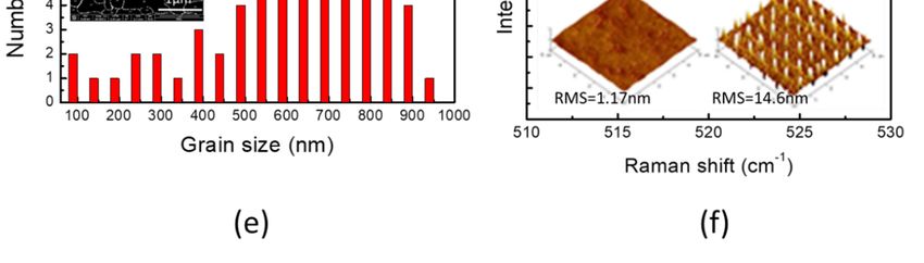
Micromachines 2020, 11, 741                                                                                   10 of 12

      To extract the threshold voltage (Vth ) and S.S. dependencies of these two types of single-grain
transistor on the gate length (Lg ), the device structures having a similar size were chosen for comparison.
The data were collected and plotted in Figure 7b. According to the result, the Vth decrease while the Lg
becomes shorter. Further, the S.S. is found to be increased with the shrinkage in Lg . It indicates that
the SCEs dominate the output characteristics at sub-100 nm of both transistors. The slower Vth roll-off
and S.S. ramp up rate in the line graph of the GAA Si NW FET elucidate that the gate-all-around
configuration has better ability in suppressing SCEs. This evidence can be found in Figure 7c as well.
The S.S. rises from 65 to 121 mV/dec. (∆S.S. = 56 mV/dec.), while the WFin increases from 10 to 50 nm
for the Ω-gate Si FETs. Comparatively, the GAA Si NW FETs reveals a lower S.S. in the same WFin and
a smaller ∆S.S. (43 mV/dec.).
      By introducing the LCG technique for monolithic 3D-ICs, we can prevent the electrical property
variation caused by the random grain size and the unpredictable boundaries. Figure 7d,e show the
cumulative plots of S.S. and Vth of the GAA Si NW FETs with and without the LCG technique within an
8-inch Si wafer. Both plots demonstrate the single-grain GAA Si NW FETs with the LCG technique have
smaller S.S. (from 19.2 to 14.7 mV/dec at FWHM) and Vth deviations (from 0.51 to 0.44 V at FWHM).
      To validate the feasibility of the monolithic 3D-IC sequential integration process, the transfer
characteristics of a GAA Si NW FET with a two-layer metal interconnect (M1-M2) were prepared
and tested before and after FIR-LA. Evidently, the lack of obvious changes in the Id -Vg behaviors
before and after the FIR-LA in Figure 7f ensures the compatibility of the monolithic 3D-IC sequential
integration process.

4. Conclusions
      In summary, novel methodologies to fabricate GAA Si NW FETs with high performance and low power
consumption were reported. By integrating the location-controlled-grain technique, laser crystallization,
far-infrared laser dopant activation, and hybrid laser-assisted salicidation, sub-50 nm GAA Si NW FETs
with lower sensitivity to Vth roll-off and subthreshold swing degradation as the gate length scaled down
were presented. Furthermore, electrical validation results provide convincing evidence for the feasibility
of monolithic three-dimensional integrated circuits. The advanced 3D architecture demonstrated in this
article enables high-bandwidth sequentially stackable circuits to achieve superior performance and low
power consumption for future mobile and neuromorphic applications.

Author Contributions: Conceptualization, T.-Y.H. and C.-C.Y.; methodology, T.-Y.H. and P.-Y.H.; software, P.-Y.H.;
validation, T.-Y.H., T.-Y.H. and C.-C.Y.; resources, C.-H.S. and J.-M.S.; data curation, T.-Y.H. and C.-C.Y.; writing—
original draft preparation, T.-Y.H.; writing—review and editing, T.-Y.H. and C.-C.Y.; supervision, W.-K.Y. and
M.-C.W.; project administration, W.-K.Y. and M.-C.W.; funding acquisition, C.-C.Y. All authors have read and
agreed to the published version of the manuscript.
Funding: The authors would like to thank the Ministry of Science and Technology (MOST 108-2221-E-492-010-)
and National Applied Research Laboratories (NARLabs) of the Republic of China for financial support.
Conflicts of Interest: The authors declare no conflict of interest.

References
1.    Schaller, R. Moore’s law: Past, present and future. IEEE Spectr. 1997, 34, 52–59. [CrossRef]
2.    Mack, C. Fifty years of Moore’s law. IEEE Trans. Semicond. Manuf. 2011, 24, 202–207. [CrossRef]
3.    Katti, G.; Stucchi, M.; De Meyer, K.; Dehaene, W. Electrical modeling and characterization of through silicon
      via for three-dimensional ICs. IEEE Trans. Electron Devices 2010, 57, 256–262. [CrossRef]
4.    Lee, M.; Wu, S.; Yang, M.; Chen, K.; Luo, G.; Lee, L.; Kao, M. High-performance Poly-Si TFTs using ultrathin
      HfSiOx gate dielectric for monolithic three-dimensional integrated circuits and system on glass applications.
      IEEE Electron Device Lett. 2010, 31, 824–826. [CrossRef]
5.    Chen, H.; Chang, C.; Lu, N.; Wu, J.; Han, M.; Cheng, Y.; Wu, Y. Characteristics of gate-all-around junctionless
      Poly-Si TFTs with an ultrathin channel. IEEE Electron Device Lett. 2013, 34, 897–899. [CrossRef]
Micromachines 2020, 11, 741 11 of 12
6. Shulaker, M.; Hills, G.; Park, R.; Roger, T.; Howe, K.; Saraswat, H.; Wong, S.M. Three-dimensional integration
of nanotechnologies for computing and data storage on a single chip. Nature 2017, 547, 74–78. [CrossRef]
7. Levinson, J.; Shepherd, F.R.; Scanlon, P.J.; Rider, M. Conductivity behavior in polycrystalline semiconductor
thin film transistors. J. Appl. Phys. 1982, 53, 1193. [CrossRef]
8. Chalmers, B. High-speed growth of sheet crystals. J. Cryst. Growth 1984, 70, 3–10. [CrossRef]
9. Sameshima, T. Laser crystallization for large-area electronics. Appl. Phys. A 2009, 96, 137–144. [CrossRef]
10. Chen, T.; Yeh, C.; Lou, J. Effects of grain boundaries on performance and hot-carrier reliability of excimer-laser
annealed polycrystalline silicon thin film transistors. J. Appl. Phys. 2004, 95, 5788–5794. [CrossRef]
11. Vandooren, A.; Franco, J. 3-D sequential stacked planar devices featuring low-temperature replacement
metal gate junctionless top devices with improved reliability. IEEE Trans. Electron Devices 2018, 65, 5165–5171.
[CrossRef]
12. Schwarzenbach, W.; Maleville, C.; Daval, N. Advanced FD-SOI and beyond low temperature SmartCut™
enables high density 3-D SoC applications. IEEE J. Electron Devices Soc. 2019, 7, 863–868. [CrossRef]
13. Ishihara, R.; Danciu, D.; Tichelaar, F.; He, M.; Hiroshima, Y.; Inoue, S.; Shimoda, T.; Metselaar, J.W.;
Beenakker, C.I.M. Microstructure characterization of location-controlled Si-islands crystallized by excimer
laser in the µ-Czochralski (grain filter) process. J. Cryst. Growth 2007, 299, 316–321. [CrossRef]
14. Ryoichi, I.; Artyom, B.; Paul, A. Location-control of large Si grains by dual-beam excimer-laser and thick
oxide portion. Jpn. J. Appl. Phys. 2000, 39, 7.
15. Ryoichi, I.; Paul, C.; Barry, D.; Metselaar, C. Property of Single-Crystalline Si TFTs Fabricated with µ-Czochralski
(grain filter) Process. SPIE Proc. 2003, 5004, 10–19.
16. Rajendran, B.; Shenoy, R.; Witte, D.; Chokshi, N.; DeLeon, R.; Tompa, G.; Pease, R. Low thermal budget
processing for sequential 3-D IC fabrication. IEEE Trans. Electron Devices 2007, 54, 707–714. [CrossRef]
17. Yang, C.; Huang, W.; Hsieh, T.; Wu, T.; Wang, H.; Shen, C.; Yeh, W.; Shiu, J.; Chen, Y.; Wu, M.; et al. High
gamma value 3D-Stackable HK/MG-Stacked Tri-Gate Nanowire Poly-Si FETs with embedded source/drain
and back gate using low thermal budget green nanosecond laser crystallization technology. IEEE Electron
Device Lett. 2016, 37, 533–536. [CrossRef]
18. Deng, F.; Johnson, A.; Asbeck, P.; Lau, S. Salicidation process using NiSi and its device application. J. Appl.
Phys. 1997, 81, 8047. [CrossRef]
19. Colgana, E.; Gambinoa, J.; Hongb, Q. Formation and stability of silicides on polycrystalline silicon. Mater. Sci.
Eng. R Rep. 1996, 16, 43–96. [CrossRef]
20. Johnson, M.; Biegelsen, D.; Moyer, M. Deuterium passivation of grain-boundary dangling bonds in silicon
thin films. Appl. Phys. Lett. 1982, 40, 882. [CrossRef]
21. Scheller, L.; Weizman, M.; Simon, P.; Fehr, M.; Nickela, N. Hydrogen passivation of polycrystalline silicon
thin films. J. Appl. Phys. 2012, 112, 63711. [CrossRef]
22. Ahn, M.; Takuya Saraya, T.; Kobayashi, M.; Sawamoto, N.; Ogura, A.; Hiramoto, T. superior subthreshold
characteristics of gate-all-around P-Type Junctionless Poly-Si nanowire transistor with ideal subthreshold
slope. Jpn. J. Appl. Phys. 2020, 59, 7. [CrossRef]
23. Mohammad, M.; Kees, B. Stacking of single-grain thin-film transistors. Jpn. J. Appl. Phys. 2009, 48, 3S2.
24. IahihR, R.; Matsumura, M. Ultra-large grain growth of Si films on glassy substrate. Electron Lett. 1995, 31, 22.
25. Aaron, M.; Voutsas, T.; Raj, S. A systematic study and optimization of parameters affecting grain size and
surface roughness in excimer laser annealed polysilicon thin films. J. Appl. Phys. 1997, 82, 4302.
26. Wu, T.; Huang, W.; Yang, C.; Chen, H.; Hsieh, T.; Lin, W.; Kao, M.; Chen, C.; Yao, J.; Jian, Y.; et al. High
performance and low power monolithic Three-Dimensional Sub-50 nm Poly Si Thin film transistor (TFTs)
circuits. Sci. Rep. 2017, 7, 1368. [CrossRef]
27. Huang, W.; Shieh, J.; Kao, M.; Shen, C.; Huang, T.; Wang, H.; Yang, C.; Hsieh, T.; Hsieh, J.; Yu, P.; et al.
Enabling N-Type Polycrystalline Ge Junctionless FinFET of Low thermal budget by in situ doping of channel
and visible pulsed laser annealing. Appl. Phys. Express 2017, 10, 026502. [CrossRef]
28. Huang, W.; Shieh, J.; Pan, F.; Yang, C.; Shen, C.; Wang, H.; Hsieh, T.; Wu, S.; Wu, M. Charge-trap non-volatile
memories fabricated by laser-enabled low-thermal budget processes. Appl. Phys. Lett. 2015, 107, 183506.
[CrossRef]
29. Yang, C.; Hsieh, T.; Huang, W.; Shen, C.; Shieh, J.; Yeh, W.; Wu, M. Recent progress in low-temperature-process
monolithic three dimension technology. Jpn. J. Appl. Phys. 2018, 57, 04FA06. [CrossRef]Micromachines 2020, 11, 741 12 of 12
30. Ouisse, T.; Cristoloveanu, S.; Borel, G. Hot-carrier-induced degradation of the back interface in short-channel
silicon-on-insulator MOSFETS. IEEE Electron Device Lett. 1991, 12, 290–292. [CrossRef]
31. Ouisse, T.; Cristoloveanu, S.; Borel, G. Electron trapping in irradiated SIMOX buried oxides. IEEE Electron
Device Lett. 1991, 12, 312–314. [CrossRef]
32. Lawrence, T.; Vinay, V.; Greg, Y. ASAP7: A 7-nm FinFET predictive process design Kit. MicroElectron J. 2016,
53, 105–115.
33. Tapas, D.; Girish, P.; Yogesh, C. Performance Evaluation of 7-nm node negative capacitance FinFET-based
SRAM. IEEE Electron Device Lett. 2017, 38, 1161–1164.
34. Singh, K.; Kumar, S.; Goel, E.; Singh, B.; Singh, P.; Baral, K.; Kumar, H.; Jit, S. Effects of source/drain elevation
and side spacer dielectric on drivability performance of non-abrupt Ultra Shallow junction gate underlap
GAA MOSFETs. Indian J. Phys. 2017, 92, 171–176. [CrossRef]
35. Yang, B.; Buddharaju, K.; Teo, S.; Singh, N.; Lo, G.; Kwong, D. Vertical silicon-nanowire formation and
Gate-All-around MOSFET. IEEE Electron Device Lett. 2008, 29, 791–794. [CrossRef]
36. Langfeld, R.; Baumann, H.; Bethge, K.; Jex, H. CO2-Laser Induced annealing and diffusion in high energy
As-ion-implanted silicon. Phys. Lett. A 1981, 82, 148–150. [CrossRef]
37. James, R. Pulsed CO2 laser annealing of silicon. Semicond. Semimet 1984, 23, 555–623.
38. Mia, S.; Jiaa, C.; Zhaob, Q.; Mantlb, S.; Urban, K. NiSi2/Si interface chemistry and epitaxial growth mode.
Acta Mater. 2009, 57, 232–236. [CrossRef]
39. Chena, H.; Linb, C.; Huang, C.; Chien, C. The effect of pulsed laser annealing on the nickel silicide formation.
Microelectron. Eng. 2010, 87, 2540–2543. [CrossRef]
© 2020 by the authors. Licensee MDPI, Basel, Switzerland. This article is an open access
article distributed under the terms and conditions of the Creative Commons Attribution
(CC BY) license (http://creativecommons.org/licenses/by/4.0/).You can also read