Light extraction in tandem organic light emitting diodes
←
→
Page content transcription
If your browser does not render page correctly, please read the page content below

Applied Physics Letters                                                                   PERSPECTIVE              scitation.org/journal/apl

    Light extraction in tandem organic light
    emitting diodes
    Cite as: Appl. Phys. Lett. 119, 060504 (2021); doi: 10.1063/5.0057325
    Submitted: 19 May 2021 . Accepted: 29 July 2021 .
    Published Online: 11 August 2021

    Xiangyu Fu,1 Shichen Yin,1 Yi-An Chen,2 Liping Zhu,1                  Qi Dong,1 Chih-Hao Chang,2             and Franky So1,a)

    AFFILIATIONS
    1
        Department of Materials Science and Engineering, North Carolina State University, Raleigh, North Carolina 27606, USA
    2
        Walker Department of Mechanical Engineering, University of Texas at Austin, Austin, Texas 78712, USA

    a)
         Author to whom correspondence should be addressed: fso@ncsu.edu

    ABSTRACT
    Since the invention of organic light emitting diodes (OLEDs), great research efforts have been dedicated to improving their efficiency and
    lifetime. For high-brightness applications, tandem OLED structures have advantages because of the lower current densities required to
    achieve high brightness. With the successful development of highly efficient charge generation layers, high brightness tandem OLEDs are
    used in displays and lighting. However, the major challenge for tandem OLEDs is the low light extraction efficiency, because about 50% of
    the light is trapped inside the device as waveguide modes. In this Perspective, we first review the recent works done on light extraction, ana-
    lyze different waveguide mode extraction structures, and then identify the key factors determining the extraction efficiencies in tandem
    OLEDs.
    Published under an exclusive license by AIP Publishing. https://doi.org/10.1063/5.0057325

    I. INTRODUCTION                                                                 Due to the limited current that can be injected into an OLED20,21
         The past three decades mark the rapid growth of mobile and            and the efficiency roll-off at high current density,22,23 single-stack
    large screen displays. Different from its precursor liquid crystal dis-    OLEDs are not sufficient to provide high luminance (>2000 cd m2)
    plays (LCDs), OLEDs are self-emissive thin film devices with lower          output for applications such as lighting,24 augmented reality display,25
    power consumption and higher contrast ratio.1 With well-developed          and other high brightness applications.26 With multiple OLED stacks
    manufacturing processes, OLEDs have become the mainstream dis-             interconnected with charge generation layers (tandem OLEDs), the
    play technology for small-sized displays such as cell phones and smart     current density required is significantly reduced through multiple pho-
    watches2 and are a strong contender for large displays such as TVs.        ton generation with several OLED units connected in series, resulting
    Nowadays, OLEDs are also used in lighting,3 head-mounted display,4,5       in enhancements in the device brightness and operating lifetime.27–30
    wearable displays,6 and medical devices.7,8                                Even with various light extraction schemes to extract the internal opti-
         Typical OLEDs consist of a metal electrode, multiple organic          cal modes as well as a substrate mode, the LEE of a tandem OLED is
    layers, and an indium tin oxide (ITO) electrode on a substrate with an     limited to about 50%.31–33 In this Perspective, we will analyze the opti-
    active OLED stack thickness less than 200 nm. For display applica-         cal modes of tandem OLEDs and discuss how to improve the LEE
    tions, top-emitting OLEDs with a transparent Mg: Ag top electrode          through light extraction structures.
    are the preferred structure to accommodate for the bottom thin film
                                                                               II. OPTICAL MODES IN TANDEM OLEDs
    transistors.9,10 In a conventional OLED, charge carriers are injected
    into the emitting layer and form excitons, which relax radiatively to            The light extraction efficiency of an OLED is limited by the opti-
    the ground state emitting photons. The ratio of the emitted photons        cal modes’ trapping photons. Because the organic layers (n  1.8), the
    and the injected charge carriers is defined as the external quantum effi-    ITO electrode (n  2), and the glass substrate (n  1.5) all have a
    ciency (EQE), which is a product of the internal quantum efficiency         higher refractive index than the air, a great fraction of light is trapped
    (IQE) and the light extraction efficiency (LEE). With the development       in the waveguide and substrate modes due to total internal reflec-
    of high quantum yield emitters11,12 with horizontal dipole orienta-        tion.34,35 In an OLED, emitters can also couple energy to the surface
    tions13–15 and charge transport layers with low refractive indices,16,17   plasmon polariton (SPP) modes, which are evanescent waves that
    the EQE of a single-stack OLED is approaching 40%.18,19                    propagate along the surface of the metal/organic interface.36,37 Only

Appl. Phys. Lett. 119, 060504 (2021); doi: 10.1063/5.0057325                                                                                 119, 060504-1
Published under an exclusive license by AIP Publishing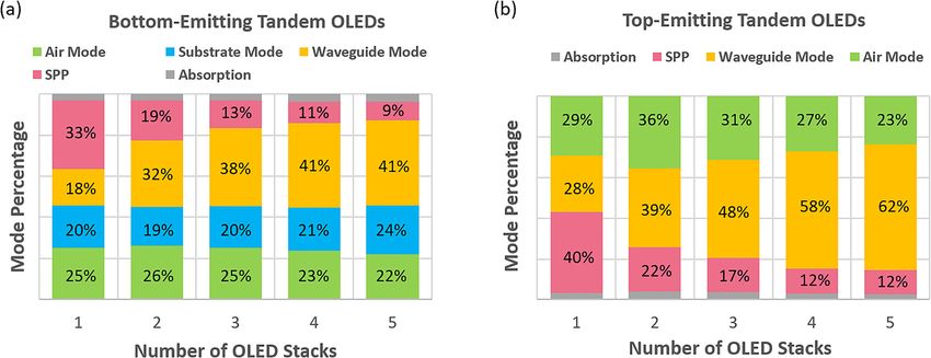
Applied Physics Letters                                                                                          PERSPECTIVE                  scitation.org/journal/apl

    photons emitted within the air cone in the normal direction become                            at the metal interface and reflection at the ITO/glass interface. A
    useful (“air mode”). The ratio of the air mode relative to all the optical                    common strategy to extract the waveguide mode is using scattering/
    modes is defined as the LEE.                                                                   diffraction or patterned interfaces to redirect the light such that it
          To maximize the LEE, the first step is to maximize the air mode                          propagates along the normal direction of the glass substrate. Due to
    density. For planar OLEDs, this is done by placing the emitting layers at                     absorption from the metal electrode, waveguide modes gradually dissi-
    the antinodes of the OLED microcavity, such that the light output is                          pate as heat as they propagate. Therefore, the efficiency of the light
    enhanced by the cavity effect.38 Since the metal electrode is a reflective                     extraction structure depends on the number of reflection paths it takes
    mirror, the cavity length is determined by the distance from the emitting                     to extract the waveguide modes. Among the different optical struc-
    layer to the metal.39–42 As the number of stack increases, the emitting                       tures, corrugated substrate, embedded scattering layer, and micro-lens
    layers are further away from the metal, and the cavity effect becomes                         array (MLA) are commonly used.
    weaker.43 Here, we use optical simulation (Setfos) to calculate the mode
    percentage of a multi-stack bottom-emitting OLED and a top-emitting                           A. Corrugated substrate
    OLED in Fig. 1. The refractive index of the capping layer is 1.8, and its
                                                                                                        In an OLED, a corrugated interface can be used for light extrac-
    thickness is 80 nm. The results show that the air mode percentage
    decreases with the number of OLED stacks with the exception of the                            tion through random or coherent scattering of the trapped light
    single-stack OLED, which has a lower LEE due to the strong SPP loss.                          [Fig. 2(a)].45 Often a micro-structure or nano-structure replicated
    For both multi-stack top and bottom emitting devices, the major loss in                       from a master mold onto an optical adhesive on a glass substrate
    LEE is due to the waveguide modes. For tandem OLEDs with more                                 through soft-imprinting is used as a substrate for OLED fabrication.
    than five stacks, the average LEE approaches 20%, slightly higher than                         The patterning process is inexpensive and scalable, but the surface
    the theoretical 15% LEE limit when the cavity effect is neglected.44                          morphology must be well controlled because any defects could result
          Since the cavity effect can only moderately improve the LEE of a                        in leakage current and device failure. Various periodic, quasi-periodic,
    tandem OLED, additional light extraction structure is needed to recover                       and random corrugated substrates have been successfully demon-
    the trapped modes. From a single-stack OLED to a tandem OLED, the                             strated in OLEDs, and over 60% LEE has been demonstrated.46
    SPP mode percentage drops from over 30% to below 10%, and the                                       The light extraction effectiveness of the corrugation depends on
    waveguide mode becomes the main light trapping channel. For bottom-                           its overlapping with the optical modes.49 In a single-stack evaporated
    emitting OLEDs, 41% of the light is trapped in the waveguide mode,                            bottom-emitting OLED, the corrugation is preserved at the metal elec-
    and 24% of the light is trapped in the substrate mode; for a top-emitting                     trode interface forming a strongly scattering interface. The electric field
    OLED, the substrate mode is eliminated, and over 60% of the light is                          of the TM waveguide modes and SPP modes both overlap strongly
    trapped in the waveguide mode. Thus, extracting the waveguide modes                           with the corrugated metal, and therefore, they can be extracted by dif-
    becomes a key factor determining the extraction efficiency.                                    fraction or scattering. In a tandem OLED, however, the thick organic
                                                                                                  stacks planarize the corrugation and lower the scattering effect from
    III. WAVEGUIDE MODE EXTRACTION                                                                the metal electrode [Fig. 2(b)].47,48 Therefore, extraction of both the
          Waveguide modes can be considered as light rays propagating                             TM waveguide and SPP modes is not effective. Instead, the extraction
    laterally while bouncing between the two electrodes due to reflection                          of the TE waveguide modes only relies on the corrugated ITO, which

     FIG. 1. The percentage of each optical mode in (a) a bottom-emitting OLED (Al/organic/ITO/glass) and (b) a top-emitting OLED (capping layer/thin Mg:Ag/organic/Ag). A
     single-color emitter (550 nm wavelength) with isotropic emitting dipoles is used for all the simulations in this article. For real emitters, the peak LEE (i.e., air mode percentage)
     is slightly reduced due to the broader emission spectrum. For emitters with higher horizontal emitting dipole ratio, the peak LEE is higher because more light is emitted toward
     the substrate normal direction.

Appl. Phys. Lett. 119, 060504 (2021); doi: 10.1063/5.0057325                                                                                                                 119, 060504-2
Published under an exclusive license by AIP Publishing
Applied Physics Letters                                                                                   PERSPECTIVE                 scitation.org/journal/apl

     FIG. 2. (a) The structures of tandem bottom-emitting OLEDs fabricated on a corrugated substrate. An external MLA is used for substrate mode extraction. (b) Cross section
     SEM image of a corrugated OLED. The total thickness of the organic layers is 200 nm. The corrugation depth on the substrate is 100 nm but is reduced to less than 20 nm at
     the metal electrode. Adapted with permission from X. Fu, Y. Mehta, and Y.-A. Chen, Adv. Mater. 33(9), 2006801 (2021).47 Copyright 2021 Wiley-VCH. (c) The influence of the
     electron transport layer thickness on the EQE of a corrugated OLED patterned with 2D TiO2 blocks. A half-ball lens is used for extracting the substrate modes. Note the
     enhancement is lower at the second antinode. Adapted with permission from Will et al., Adv. Funct. Mater. 29(20) 1901748 (2019).Copyright 2019 Wiley-VCH.

    has very limited scattering strength due to the shallow corrugation                      etching selectivities and periodicities. Therefore, fine control of nano-
    depth of the ITO electrode, as well as the small index contrast between                  structures’ geometry is possible. Combining with the roll-to-roll sys-
    ITO and the adjacent organic layer and the glass substrate. In general,                  tem, Langmuir–Blodgett assembly of colloidal nanospheres might be a
    the light extraction efficiency of the corrugated substrate is lower with                 method for volume manufacturing with fine control of a nanostruc-
    thicker organic layers [Fig. 2(c)].48 To improve the light scattering                    ture patterning process.
    from the corrugated ITO, a low refractive index layer or embedded air                          Random corrugated structures can be fabricated by techniques
    tunnels can be inserted between the ITO and the glass substrate to                       such as polymer phase separation65,66 and spontaneous formation
    increase the index contrast.50                                                           through de-wetting67 or buckling.68 Among these methods, spontane-
          There are only a handful of reports applying corrugated sub-                       ously formed buckling patterns can be produced by a thermally evapo-
    strates on tandem OLEDs. Ou et al. used quasi-periodic nanocone                          rating process and does not require further etching process, thus the
    arrays and demonstrated a 50.4% EQE on a two-stack tandem                                most suitable for large-area substrate manufacturing.
    OLED.31 The nanocone arrays are fabricated on a spin-coated                                    For effective light extraction, the corrugation geometry is impor-
    PEDOT:PSS layer on top of an ITO coated substrate using soft nano-                       tant. While corrugation is effective for single stack OLEDs, its effec-
    imprint lithography. Li et al. demonstrated 76.3% EQE in a two-stack                     tiveness for tandem OLEDs is limited. To be effective for light
    tandem white OLED using a lithography-free patterning approach.32                        extraction in tandem OLEDs, the corrugation profile must be deep
    The wrinkling pattern can be directly created on the substrate by reac-                  enough for effective light scattering. A deep corrugation profile would
    tive ions etching (RIE) on poly(dimethylsiloxane) (PDMS), leading to                     lead to device failure, and therefore, a non-planar surface for light
    a broad periodicity distribution and an average depth of 150 nm.                         extraction for tandem OLEDs is not practical.
          For manufacturing, the corrugated substrate fabrication process
    must be inexpensive and scalable. This rules out high precision pat-                     B. Embedded scattering layer
    terning techniques such as electron-beam lithography51 and two-                                Recent research works in light extraction of tandem OLEDs have
    photon photopolymerization.52 Laser interference lithography53–56                        focused on using planar substrates with embedded light extraction
    and holographic interference57 are effective methods to pattern peri-                    structures to extract the waveguide modes. An embedded scattering
    odic structures with nanoscale accuracy. However, they are also diffi-                    layer can be fabricated by starting with a corrugated substrate and
    cult to scale up, because they usually require sophisticated laser                       then planarizes it with a higher index spacer [Fig. 3(a)]. In this struc-
    equipment setup and accurate alignment. In addition, most of the                         ture, the average refractive index of the embedded scattering layer
    techniques discussed above use photoresists as etching masks with low                    needs to be the same or higher than the adjacent layer (organic layer
    etching selectivity and limited corrugation depth.                                       and ITO), such that the waveguide modes can be coupled from the
          Another way to fabricate quasi-periodic structures is by                           OLED stack into the spacer layer for scattering.69
    Langmuir–Blodgett assembly of colloidal nanospheres.58–60 The peri-                            To efficiently extract the waveguide modes, the interface of the
    odicity can be defined by applying one or multiple sizes of nano-                         scattering layer needs to be rough for light incident at large angles to
    spheres.61 This method can be further introduced to a roll-to-roll                       be extracted, and the absorption inside the tandem OLED must be
    system for continuous structures patterning followed by an RIE pro-                      minimized while the emitting light propagating within the OLED
    cess for volume fabrication.62–64 Self-assembled colloidal nanospheres                   stack. For a quantitative analysis, we use 3D ray tracing (Setfos 5.1) to
    can be made from polymer-based materials such as polystyrene,                            simulate the LEE of tandem OLEDs fabricated on embedded scattering
    oxide-based materials such as silicon oxide, and other materials. This                   layers [Fig. 3(b)]. We compare different surface roughness root mean
    process allows the choice of etching mask materials with different                       square (RMS) of two typical metal electrodes, Al and Ag, which

Appl. Phys. Lett. 119, 060504 (2021); doi: 10.1063/5.0057325                                                                                                       119, 060504-3
Published under an exclusive license by AIP Publishing
Applied Physics Letters                                                                                    PERSPECTIVE                 scitation.org/journal/apl

     FIG. 3. (a) Schematic drawing of a tandem OLED fabricated on an embedded scattering layer. Two light rays are shown incident on the scattering layer with different surface
     roughnesses. (b) The dependence of the LEE on the roughness of the scattering layer in a three-stack OLED. Comparisons are made between Al and Ag as the top electrode,
     and with or without an external MLA. (c) The dependence of the LEE and ITO transmittance on the ITO electrode absorption in a tandem OLED. In tandem OLEDs, the absorp-
     tion is mainly contributed by the metal and the ITO electrode.

    absorbs 15% and 6% of the incident light from an organic layer,                          only 100 nm, but a 1% increase in its extinction coefficient would
    respectively.                                                                            result in a 15% loss in the LEE while the substrate transmittance is
          For tandem OLEDs with an Al cathode, the LEE is improved                           only reduced by 1% [Fig. 3(c)]. This puts a strict requirement on the
    from 25% to 55% as the RMS increases from 0 to 1.5 lm, which comes                       choice of the high index spacer, which is often over 1 lm thick to effi-
    from the stronger scattering of the waveguide modes. Further incre-                      ciently couple the waveguide modes while planarizing the light scatter-
    ment in the RMS only improves the LEE marginally toward 58%.                             ing layer. Furthermore, the fabrication of the embedded scattering
    When an external MLA is used for extraction, light can more easily                       layer poses another challenge. To realize the LEE potential, the RMS
    escape the substrate, and the LEE is further improved to 63%. Note                       roughness of the corrugated substrate needs to be larger than 0.5 lm,
    that after attaching an external MLA, the LEE plateau is reduced from                    which would diffuse 90% of the incident light and appear very hazy.
    1 to 0.5 lm. This is because without the external MLA, the scattering                    Typical processing approaches cannot achieve such a large roughness.
    strength of the scattering layer needs to be strong enough to extract                          Alternatively, the scattering effect can be improved by increasing
    the substrate mode.                                                                      the index contrast between the high index spacer (“host”) and the low
          When the top electrode is replaced with Ag, the absorption loss                    index particles (“dopant”), which often involves introducing voids in
    from each reflection on the metal is reduced by more than a half. This                    an inorganic material. Qu et al. fabricated a TiO2 layer with air grids
    greatly extends the lifespan of the waveguide mode, allowing it to have                  under the ITO electrode through a combination of photolithography
    more chances to be extracted by the scattering layer. As a result, the                   and wafer bonding [Fig. 4(a)].70 The structure efficiently extracts the
    LEE of a tandem OLED without/with the external MLA is improved                           waveguide modes without compromising the electrical properties of
    to 75% and 85%, respectively.                                                            the OLED. Jeon et al. used plasma-enhanced chemical vapor deposi-
          The theoretical 85% peak LEE assumes that light is only absorbed                   tion (PECVD) to deposit a high-index Si3N4 film and then dry-etched
    by the metal electrode. In practice, the organic layers, ITO, and a high                 the film to form vacuum nanohole arrays [Fig. 4(b)].69,72 The structure
    index spacer also have residual light absorption, which is significant                    enhanced the EQE of a single-stack OLED from 20.5% to 78% with a
    for the waveguide mode, due to its longer lateral propagation length                     half-full lens attached, owing to the large depth of the vacuum nano-
    within the OLED. For example, the thickness of the ITO electrode is                      holes. Recently, Han et al. demonstrated a more feasible method to

     FIG. 4. (a) Schematic cut-away view of an OLED with a sub-anode grid. Reproduced with permission from Qu et al., Nat. Photonics 9(11), 758–763 (2015). Copyright 2015
     Nature Publishing Group. (b) Cross-sectional scanning transmission electron microscopy image of a white OLED fabricated on top of the embedded vacuum nanohole arrays.
     Reproduced with permission from Jeon et al., “Adv. Opt. Mater. 6(8), 1701349 (2018). Copyright 2018 Wiley-VCH. (c) Schematic illustration of light extraction in OLEDs by
     nano-particle based scattering layers. Reproduced with permission from H. Chang, J. Lee, and S. Hofmann, J. Appl. 113(20), 204502 (2013).71 Copyright 2013 AIP Publishing.

Appl. Phys. Lett. 119, 060504 (2021); doi: 10.1063/5.0057325                                                                                                        119, 060504-4
Published under an exclusive license by AIP Publishing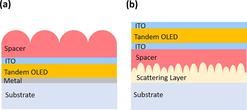
Applied Physics Letters                                                                                 PERSPECTIVE              scitation.org/journal/apl

    form hollows inside a TiO2 spacer by nanoimprinting of a polymer                         high index (n > 1.8) polymers have an absorption onset at
    layer and planarizing with TiO2 nano-particles.33 During the thermal                     420–430 nm, which makes these high index polymers unsuitable for
    annealing, the polymer is removed, leaving a hollow nanostructure in                     OLED light extraction.76,77 With advances in high index polymer
    the TiO2 layer. The hollow structure improved the EQE of a two-stack                     design, we can expect a broader selection of polymers for OLED light
    tandem OLED from 82.5% and 103% with the substrate mode                                  extraction.
    extracted by attaching a half-full lens. Nonetheless, processing inor-
    ganic materials to form air gaps is not compatible with large-area
                                                                                             C. Micro-lens array
    panel manufacturing.
          In comparison, solution processable materials, such as high index                        High index micro-lens arrays (MLAs) are also used to extract the
    polymers, are less expensive and more compatible with roll-to-roll fab-                  substrate and waveguide modes [Fig. 5(a)]. A typical MLA has a diam-
    rication. Chang et al. demonstrated a TiO2 nano-particle based poly-                     eter on the scale of micrometers, much larger than the wavelength of
    mer scattering layer for waveguide mode extraction and achieved 46%                      light, and therefore, we can use simple ray tracing to analyze the optics.
    EQE in a single-stack OLED with a glass half-ball lens [Fig. 4(c)].71                    Because the micro-lens unit is much smaller than an OLED device,
    Preinfalk et al. demonstrated a similar TiO2/polymer scattering layer                    light is incident onto the curved MLA surface at random locations,
    on large areas via screen printing.73 Kim et al. fabricated an OLED on                   thus reflected/refracted at random angles.
    top of a polyethylene naphthalate (PEN) substrate, having a high index                         Although the feature-size of an embedded MLA is much larger
    polymer (n ¼ 1.7) filled with organic or inorganic filler particles.74 The                 than an embedded scattering layer, they both function as a scattering
    substrate mode and the waveguide mode can be extracted by scattering                     layer compared to an OLED device. In Fig. 5(a), we consider a set of
    using filler particles. Despite the potential low-cost processing, the                    parallel light rays incident on a hemispherical MLA from the high
    refractive indices of optical polymers are limited to n < 1.8 along with                 index layer. Because a small shift of the incident ray, ray 1 and ray 2
    residual absorption in the visible range. A summary of the transparent                   are transmitted/reflected toward different angles, and ray 3 is reflected
    high index materials demonstrated in OLEDs is given in Table I. Some                     back toward the metal electrode after several total internal reflections.
    potential high index materials are also listed. Recently, polymeric car-                 The average results of random incident angles and sites are similar to
    bon nitride (pCN), which is transparent in the most visible range, with                  random scattering and, thus, can be represented as ray 4.
    a high index of 2.27 has been successfully deposited on a large sub-                           We simulate the LEE of a tandem OLED fabricated on an
    strate through chemical vapor deposition.75 However, most of the                         embedded MLA and vary the aspect ratios (height/radius) from 0 to 1

    TABLE I. List of high refractive index materials used in OLED fabrication.

                                                    Refractive index
    Host materials            Nano-particles         (host/dopant)                         Processing                       EQE or enhancement              Reference

    Si3N4                         Vacuum                  2.02/1.0                 PECVD onto nanoimprinted                   50% enhancement                   78
                                                                                        polymer pillar arrays
    Si3N4                         Vacuum                  2.02/1.0               Dry-etching the Si3N4 PECVD film          78% (with a half-full lens)           69
                                                                                  then anodic bonding the film to
                                                                                               glass
    Zr2O                            MgO                  1.84/1.73                      E-beam evaporation                  34.7% enhancement                   79
    Resin                           SiOx                 1.81/1.5                   Nano-coned SiOX formed by              65.3% (with a wrinkle                80
                                                                                            dry-etching                     structure to extract
                                                                                                                              substrate mode)
    a)
         TiO2                     Vacuum                  2.0/1.0             Spin-coating TiO2 NPs and sol onto         103% (white tandem OLED                33
                                                                                the thermal-imprinted substrate             with a half-full lens)
                                                                                      then anneal at 500  C
    Polymer                      TiO2 NPs                 1.5/2.0             TiO2 NPs dispersed in the monomer               56% enhancement                   73
                                                                                  solution of polymer and then
                                                                                    screen-printing the blend
    NOA 73                       TiO2 NPs                 1.56/2.0               TiO2 NPs in NOA 73 and then                          56%                       81
                                                                                          spin-coating
    NOA 170                                                  1.7                          Spin-coating                                37%                       82
    BDAVBi                                               1.9                            Evaporation                                NA                        77
    poly(BTVS)                                           1.74                          Spin-coating                                NA                        83
    polymeric carbon                                     2.27              Thermal-chemical-vapor-deposition                       NA                        75
    nitride (pCN)
    SBDDVE                                               1.91                 Sulfur chemical vapor deposition                     NA                        76
    a)
      The TiO2 is processed from the TiO2 NPs dispersed resin and TiO2 sol.

Appl. Phys. Lett. 119, 060504 (2021); doi: 10.1063/5.0057325                                                                                               119, 060504-5
Published under an exclusive license by AIP Publishing
Applied Physics Letters                                                                                   PERSPECTIVE                 scitation.org/journal/apl

     FIG. 5. (a) Schematic drawing of an embedded MLA with hemispherical lens shape for waveguide extraction. Also shown is a set of parallel light rays incident on the embed-
     ded MLA at different locations. (b) Dependence of the LEE on the aspect ratio of the MLA. Comparisons are made for Al/Ag electrodes and with/without an external MLA. (c)
     Schematic illustration of devices on a sub-electrode MLA substrate. Reproduced with permission from Qu et al., ACS Photonics 5, 2453–2456 (2018).84 Copyright 2018
     American Chemical Society.

    [Fig. 5(b)]. Note that the LEE has a very similar dependence on the                      fragile, the placement of the light extraction structures can be challeng-
    aspect ratio as on the roughness of a scattering layer. Here, an MLA                     ing. It also rules out high index materials that require spin-coating or
    with a high aspect ratio is better bending the light ray. In addition,                   high temperature annealing, which is often used to create embedded
    when an Ag electrode and an external MLA are used, the LEE can                           scattering layers. In comparison, MLAs can be independently fabri-
    reach 85%, the same value as a scattering layer with over 1 lm rough-                    cated and attached on the top-emitting OLED [Fig. 6(a)].
    ness RMS.                                                                                      Fabricating an MLA on top of an OLED requires special care.
          An MLA index-matched with glass is often used for substrate                        Thomschke et al. evaporated thin organic on the MLA and then fused
    mode extraction. Reineke et al. used a high-index glass substrate with                   it with the OLED device by low temperature annealing.86 Kim et al.
    MLAs to extract both the waveguide mode and the substrate mode.85                        evaporated organic materials through a metal mesh with micrometer-
    However, a high-index glass is costly since containing rare-earth ele-                   size holes to directly form MLAs on an OLED. The shape of the MLA
    ments.74 Only recently, Qu et al. demonstrated a sub-electrode MLA                       is controlled by the evaporation rate, which offers high aspect ratios
    for waveguide mode extraction [Fig. 5(c)].84 The sub-electrode layer                     for light extraction.87
    consists of a polymer spacer layer (NOA 170, n ¼ 1.7) on top of a hex-                         Alternatively, we can use ITO/IZO for both electrodes and embed
    agonal closed-packed array of 10 lm diameter hemispherical MLA.                          a reflective light extraction structure under the device [Fig. 6(b)]. Qu
    With both an internal and external MLAs, the waveguide and sub-                          et al. demonstrated an improved LEE using a reflective sub-electrode
    strate modes are efficiently extracted, leading to a 47% EQE; with an                     grid88 and then improved the design using a diffusive dielectric reflec-
    index matching fluid to fully extract the substrate mode, the EQE is                      tor to reduce the light absorption.82 In these two structures, the wave-
    further improved to 70%.                                                                 guide modes are scattered randomly at the uneven surfaces, and those
                                                                                             scattered light toward the normal direction can be extracted. The
                                                                                             advantage of using a spacer structure is compatible with the bottom-
    D. Light extraction in top-emitting tandem OLEDs                                         up manufacturing of OLED panels. In addition, depending on the
         The waveguide mode extraction strategies above apply to top-                        scattering strength and the spacer thickness, the waveguide modes can
    emitting OLEDs as well, but because the organic thin films are very                       propagate for several micrometers before being extracted, causing

                            FIG. 6. The structures of tandem top-emitting OLEDs with (a) an MLA on the top spacer and (b) an embedded scattering layer.

Appl. Phys. Lett. 119, 060504 (2021); doi: 10.1063/5.0057325                                                                                                       119, 060504-6
Published under an exclusive license by AIP Publishing
Applied Physics Letters PERSPECTIVE scitation.org/journal/apl
10
haziness from the pixels. In solid-state lightning, haze is not an issue S. Kwon, E.-H. Lee, K. Kim et al., “Efficient micro-cavity top emission OLED
since the OLED panel is orders larger than the spacer thickness; in dis- with optimized Mg:Ag ratio cathode,” Opt. Express 25(24), 29906 (2017).
11
S. F. Wu, S. H. Li, Y. K. Wang et al., “White organic LED with a luminous effi-
plays, however, hazy pixels could affect the image quality.
cacy exceeding 100 l m W1 without light out-coupling enhancement
IV. SUMMARY techniques,” Adv. Funct. Mater. 27(31), 1–9 (2017).
12
M. Zhang, W. Liu, C. Zheng et al., “Tricomponent exciplex emitter realizing
The pursuit of high efficiency OLEDs remains a challenge, and over 20% external quantum efficiency in organic light-emitting diode with mul-
with the increasing demand for high brightness light sources, tandem tiple reverse intersystem crossing channels,” Adv. Sci. 6(14), 1801938 (2019).
13
OLEDs will be in demand for their performance. In this Perspective, C.-Y. Lu, M. Jiao, W.-K. Lee et al., “Achieving above 60% external quantum
we review the design of tandem OLEDs and the limitation on its light efficiency in organic light-emitting devices using ITO-free low-index transpar-
ent electrode and emitters with preferential horizontal emitting dipoles,” Adv.
extraction efficiency (LEE) due to strong waveguide mode loss. We
Funct. Mater. 26(19), 3250–3258 (2016).
then compare different waveguide mode extraction structures includ- 14
J. Frischeisen, D. Yokoyama, A. Endo, C. Adachi, and W. Br€ utting, “Increased
ing corrugated substrates, embedded scattering layers, and micro-lens light outcoupling efficiency in dye-doped small molecule organic light-emitting
arrays, based on a common mechanism of redirecting the trapped light diodes with horizontally oriented emitters,” Org. Electron. 12(5), 809–817
toward the normal direction. We compare the fabrication methods for (2011).
15
each structure and conclude that an embedded micro-lens array is the K. H. Kim, S. Lee, C. K. Moon et al., “Phosphorescent dye-based supramole-
most cost-effective structure for light extraction in large-area OLED cules for high-efficiency organic light-emitting diodes,” Nat. Commun. 5, 1–8
(2014).
panels. Using optical simulation, we identified that the key to achieve 16
H. Shin, J. H. Lee, C. K. Moon, J. S. Huh, B. Sim, and J. J. Kim, “Sky-blue phos-
high LEEs is to lower the absorption loss using highly transparent and phorescent OLEDs with 34.1% external quantum efficiency using a low refrac-
high index materials and to reduce the reflection paths it takes to tive index electron transporting layer,” Adv. Mater. 28, 4920–4925 (2016).
17
extract the waveguide mode using light extraction structures with a C. Fuchs, P.-A. Will, M. Wieczorek et al., “Enhanced light emission from top-
high aspect ratio. With optimal spacer materials and light extraction emitting organic light-emitting diodes by optimizing surface plasmon polariton
structures, the LEE of tandem OLEDs can be enhanced by more than losses,” Phys. Rev. B 92, 245306 (2015).
18
T. Lin, T. Chatterjee, W. Tsai, W. Lee, M. Wu, and M. Jiao, “Sky-blue organic
three times. This will significantly reduce the power consumption, light emitting diode with 37% external quantum efficiency using thermally acti-
making tandem OLEDs the most promising candidate for solid-state vated delayed fluorescence from spiroacridine-triazine hybrid,” Adv. Mater.
lighting and other high brightness applications. 28(32), 6976–6983 (2016).
19
T. Watabe, R. Yamaoka, N. Ohsawa, and A. Tomida, “Extremely high-efficient
OLED achieving external quantum efficiency over 40% by carrier injection
ACKNOWLEDGMENTS
layer with super-low refractive index,” in SID Symposium Digest of Technical
The authors acknowledge the support of the Department of Papers (SID, 2018), Vol. 49, pp. 332–335.
20
S. Scholz, D. Kondakov, and K. Leo, “Degradation mechanisms and reactions
Energy Solid State Lighting program (Award No. DE-FOA-
in organic light-emitting devices,” Chem. Rev. 115(16), 8449–8503 (2015).
0001823). 21
K. Sawabe, M. Imakawa, M. Nakano, T. Yamao, and S. Hotta, “Current-
DATA AVAILABILITY confinement structure and extremely high current density in organic light-
emitting transistors,” Adv. Mater. 24(46), 6141–6146 (2012).
The data that support the findings of this study are available 22
N. C. Giebink and S. R. Forrest, “Quantum efficiency roll-off at high brightness
within the article. in fluorescent and phosphorescent organic light emitting diodes,” Phys. Rev. B
77(12), 125215 (2008).
23
C. Murawski, K. Leo, and M. C. Gather, “Efficiency roll-off in organic light-
REFERENCES emitting diodes,” Adv. Mater. 25(47), 6801–6827 (2013).
1 24
H. W. Chen, J. H. Lee, B. Y. Lin, S. Chen, and S. T. Wu, “Liquid crystal display F. So, J. Kido, and P. Burrows, “Organic light-emitting devices for solid-state
and organic light-emitting diode display : Present status and future lighting introduction: The potential for,” MRS Bulletin 33, 663–669 (2008).
25
perspectives,” Light: Sci. Appl. 7(3), 17168 (2018). Y. Lin, P. Chen, K. Chen et al., “Highly transparent AMOLED for augmented
2
V. C. Coffey, “The age of OLED displays,” Opt. Photonics News 28(11), 34–41 reality applications,” in SID Symposium Digest of Technical Papers (SID, 2018),
(2017). pp. 621–623.
3 26
Q. D. Ou, L. Zhou, Y. Q. Li et al., “Extremely efficient white organic light- J. Song, H. Lee, E. G. Jeong, K. C. Choi, and S. Yoo, “Organic light-emitting
emitting diodes for general lighting,” Adv. Funct. Mater. 24(46), 7249–7256 diodes: pushing toward the limits and beyond,” Adv. Mater. 32, 1907539:1–17
(2014). (2020).
4 27
P. Cipresso, I. Alice, C. Giglioli, M. A. Raya, and G. Riva, “The past, present, C. W. Chu, C. W. Chen, S. H. Li, E. H. E. Wu, and Y. Yang, “Integration of
and future of virtual and augmented reality research: A network and cluster organic light-emitting diode and organic transistor via a tandem structure,”
analysis of the literature,” Front. Psychol. 9, 1–20 (2018). Appl. Phys. Lett. 86(25), 253503 (2005)
5 28
Y.-H. Lee, T. Zhan, and S. T. Wu, “Prospects and challenges in augmented L. S. Liao, K. P. Klubek, and C. W. Tang, “High-efficiency tandem organic
reality displays,” Virtual Realilty Intell. Hardware 1(1), 10–20 (2019). light-emitting diodes,” Appl. Phys. Lett. 84(2), 167 (2008).
6 29
Y. J. Song, J. Kim, H. Cho et al., “Fibertronic organic light-emitting diodes M. Fung, Y. Li, and L. Liao, “Tandem organic light-emitting diodes,” Adv.
toward fully addressable, environmentally robust, wearable displays,” ACS Mater. 28(47), 10381–10408 (2016).
30
Nano 14(1), 1133–1140 (2020). P. Xiao, J. Huang, Y. Yu, and B. Liu, “Recent developments in tandem white
7
J. T. Smith, S. Member, B. A. Katchman et al., “Application of flexible OLED organic light-emitting diodes,” Molecules 24(1), 151 (2019).
31
display technology to point-of-care medical diagnostic testing,” J. Disp. Q. Ou, L. Zhou, Y. Li et al., “Simultaneously enhancing color spatial unifor-
Technol. 12(3), 273–280 (2016). mity and operational stability with deterministic quasi-periodic nanocone
8
Y. Jeon, H. Choi, M. Lim et al., “A wearable photobiomodulation patch using a arrays for tandem organic light-emitting diodes,” Adv. Opt. Mater. 3(1), 87-94
flexible red-wavelength OLED and its in vitro differential cell proliferation (2015).
32
effects,” Adv. Technol. 3(5), 1700391 (2018). Y. Li, M. Kovac, J. Westphalen et al., “Tailor-made nanostructures bridging
9
C. W. Tang and S. A. VanSlyke, “Organic electroluminescent diodes,” Appl. chaos and order for highly efficient white organic light-emitting diodes,” Nat.
Phys. Lett. 51(12), 913–915 (1987). Commun. 10, 2972 (2019).
Appl. Phys. Lett. 119, 060504 (2021); doi: 10.1063/5.0057325 119, 060504-7
Published under an exclusive license by AIP PublishingApplied Physics Letters PERSPECTIVE scitation.org/journal/apl
33 59
K. Han, K. Kim, Y. Han et al., “Highly efficient tandem white OLED using a N. D. Denkov, O. D. Velev, P. A. Kralchevsky, I. B. Ivanov, H. Yoshimura, and
hollow structure,” Adv. Mater. Interfaces 7(9), 1901509 (2020). K. Nagayama, “Two-dimensional crystallization,” Nature 361(6407), 26
34
M. C. Gather and S. Reineke, “Recent advances in light outcoupling from white (1993).
60
organic light-emitting diodes,” J. Photon Energy 5(1), 057607 (2015). A. van Blaaderen, R. Ruel, and P. Wiltzius, “Template-directed colloidal crys-
35
A. Salehi, X. Fu, D. Shin, and F. So, “Recent advances in OLED optical design,” tallization,” Nature 385(6614), 321–324 (1997).
61
Adv. Funct. Mater. 29, 1808803 (2019). W. H. Koo, W. Youn, P. Zhu, X. H. Li, N. Tansu, and F. So, “Light extraction
36
W. L. Barnes, A. Dereux, and T. W. Ebbesen, “Surface plaston subwavelength of organic light emitting diodes by defective hexagonal-close-packed array,”
optics,” Nature 424(6950), 824–830 (2003). Adv. Funct. Mater. 22(16), 3454–3459 (2012).
37 62
B. J. Scholz, J. Frischeisen, A. Jaeger, D. S. Setz, T. G. Reusch, and W. Br€
utting, X. Li and J. F. Gilchrist, “Large-area nanoparticle films by continuous auto-
“Extraction of surface plasmons in organic light-emitting diodes via high-index mated Langmuir–Blodgett assembly and deposition,” Langmuir 32(5),
coupling,” Opt. Express 20(S2), A205 (2012). 1220–1226 (2016).
38 63
T.-Y. Cho, C.-L. Lin, and C.-C. Wu, “Microcavity two-unit tandem organic M. Parchine, J. McGrath, M. Bardosova, and M. E. Pemble, “Large area 2D and
light-emitting devices having a high efficiency,” Appl. Phys. Lett. 88(11), 3D colloidal photonic crystals fabricated by a roll-to-roll Langmuir-Blodgett
111106 (2006). method,” Langmuir 32(23), 5862–5869 . (2016).
39
V. B. Khalfin, G. Gu, and P. E. Burrows, “Weak microcavity effects in organic 64
I.-T. Chen, E. Schappell, X. Zhang, and C.-H. Chang, “Continuous roll-to-roll
light-emitting devices,” Phys. Rev. B 58(7), 3730–3740 (1998). patterning of three-dimensional periodic nanostructures,” Microsyst. Nanoeng.
40
S. Hofmann, M. Thomschke, P. Freitag, M. Furno, B. L€ ussem, and K. Leo, 6(1), 22 (2020).
“Top-emitting organic light-emitting diodes: Influence of cavity design,” Appl. 65
K. Tanaka, A. Takahara, and T. Kajiyama, “Film thickness dependence of the
Phys. Lett. 97, 253308 (2010). surface structure of immiscible polystyrene/poly(methyl methacrylate) blends,”
41
J. Lee, N. Chopra, and F. So, “Cavity effects on light extraction in organic light Macromolecules 29(9), 3232–3239 (1996).
emitting devices,” Appl. Phys. Lett. 92, 033303 (2008). 66
B. Jiao, Y. Yu, Y. Dai, X. Hou, and Z. Wu, “Improvement of light extraction in
42
J. Lee, T. H. Han, M. H. Park et al., “Synergetic electrode architecture for effi- organic light-emitting diodes using a corrugated microcavity,” Opt. Express
cient graphene-based flexible organic light-emitting diodes,” Nat. Commun. 7, 23(4), 4055 (2015).
1–9 (2016). 67
J. W. Shin, D. H. Cho, J. Moon et al., “Random nano-structures as light extrac-
43
H. Benisty, H. D. Neve, and C. Weisbuch, “Impact of planar microcavity effects tion functionals for organic light-emitting diode applications,” Org. Electron.
on light extraction—Part I: Basic concepts and analytical trends,” IEEE J. 15(1), 196–202 (2014).
Quantum Electron. 34(9), 1612–1631 (1998). 68
W. H. Koo, S. M. Jeong, F. Araoka et al., “Light extraction from organic light-
44
W. Br€ utting, J. Frischeisen, T. D. Schmidt, B. J. Scholz, and C. Mayr, “Device emitting diodes enhanced by spontaneously formed buckles,” Nat. Photonics
efficiency of organic light-emitting diodes: Progress by improved light out-
4(4), 222–226 (2010).
coupling,” Phys. Status Solidi A 210(1), 44–65 (2013). 69
45 S. Jeon, S. Lee, K. H. Han et al., “High-quality white OLEDs with comparable
J. M. Lupton, B. J. Matterson, I. D. W. Samuel, M. J. Jory, and W. L. Barnes,
efficiencies to LEDs,” Adv. Opt. Mater. 6(8), 1701349 (2018).
“Bragg scattering from periodically microstructured light emitting diodes,” 70
Y. Qu, M. Slootsky, and S. R. Forrest, “Enhanced light extraction from organic
Appl. Phys. Lett. 77(21), 3340–3342 (2000).
46 light-emitting devices using a sub-anode grid,” Nat. Photonics 9(11), 758–763
W. Youn, J. Lee, M. Xu, R. Singh, and F. So, “Corrugated sapphire substrates
(2015).
for organic light-emitting diode light extraction,” ACS Appl. Mater. Interfaces 71
H. Chang, J. Lee, and S. Hofmann, “Nano-particle based scattering layers for
7(17), 8974–8978 (2015).
47 optical efficiency enhancement of organic light-emitting diodes and organic
X. Fu, Y. Mehta, and Y.-A. Chen, “Directional polarized light emission from
solar cells,” J. Appl. 113(20), 204502 (2013).
thin-film light-emitting diodes,” Adv. Mater. 33(9), 2006801 (2021). 72
48 S. Jeon, J. H. Lee, J. H. Jeong et al., “Vacuum nanohole array embedded phos-
P. Will, M. Schmidt, K. Eckhardt et al., “Efficiency of light outcoupling struc-
phorescent organic light emitting diodes,” Sci. Rep. 5, 8685 (2015).
tures in organic light-emitting diodes: 2D TiO2 array as a model system,” Adv. 73
J. B. Preinfalk, T. Eiselt, T. Wehlus et al., “Large-area screen-printed internal
Funct. Mater. 29(20) 1901748 (2019).
49
N. Danz, D. Michaelis, C. W€achter, N. Danz, D. Michaelis, and C. W€achter, extraction layers for organic light-emitting diodes,” ACS Photonics 4(4),
“Light extraction from OLEDs: the waveguide perspective Light exctraction 928–933 (2017).
74
from OLEDs—The waveguide perspective,” Proc. SPIE 6475, 64750J (2007). E. Kim, H. Cho, K. Kim et al., “A facile route to efficient, low-cost flexible
50
Y. S. Shim, J. H. Hwang, C. H. Park, S.-G. Jung, Y. W. Park, and B.-K. Ju, “An organic light-emitting diodes: Utilizing the high refractive index and built-in
extremely low-index photonic crystal layer for enhanced light extraction from scattering properties of industrial-grade PEN substrates,” Adv. Mater. 27(9),
organic light-emitting diodes,” Nanoscale 8(7), 4113–4120 (2016). 1624–1631 (2015).
75
51
T. H. P. Chang, M. Mankos, K. Y. Lee, and L. P. Muray, “Multiple electron- P. Giusto, D. Cruz, T. Heil et al., “Shine bright like a diamond: New light
beam lithography,” Microelectron. Eng. 57–58, 117–135 (2001). on an old polymeric semiconductor,” Adv. Mater. 32(10), 1908140
52
S. Maruo, O. Nakamura, and S. Kawata, “Three-dimensional microfabrication with (2020).
76
two-photon-absorbed photopolymerization,” Opt. Lett. 22(2), 132–134 (1997). D. H. Kim, W. Jang, K. Choi et al., “One-step vapor-phase synthesis of trans-
53
C. V. Shank and R. V. Schmidt, “Optical technique for producing 0.1-l peri- parent high refractive index sulfur-containing polymers,” Sci. Adv. 6(28),
odic surface structures,” Appl. Phys. Lett. 23(3), 154–155 (1973). eabb5320 (2020).
77
54
H. I. Smith, “Low cost nanolithography with nanoaccuracy,” Physica E D. Yokoyama, K. Otani, T. Nakayama, and J. Kido, “Wide-range refractive
11(2–3), 104–109 (2001). index control of organic semiconductor films toward advanced optical
55 design of organic optoelectronic devices,” Adv. Mater. 24(47), 6368–6373
A. Bagal and C.-H. Chang, “Fabrication of subwavelength periodic nanostruc-
tures using liquid immersion Lloyd’s mirror interference lithography,” Opt (2012).
78
Lett. 38(14), 2531–2534 (2013). S. Jeon, J.-W. Kang, H.-D. Park et al., “Ultraviolet nanoimprinted polymer
56 nanostructure for organic light emitting diode application,” Appl. Phys. Lett.
Y.-A. Chen, S. V. Naidu, Z. Luo, and C.-H. Chang, “Enhancing optical trans-
mission of multilayer composites using interfacial nanostructures,” J. Appl. 92(22), 223307 (2008).
79
Phys. 126(6), 63101 (2019). K. Hong, H. K. Yu, I. Lee, K. Kim, S. Kim, and J.-L. Lee, “Enhanced light
57 out-coupling of organic light-emitting diodes: spontaneously formed
M. Campbell, D. N. Sharp, M. T. Harrison, R. G. Denning, and A. J.
Turberfield, “Fabrication of photonic crystals for the visible spectrum by holo- nanofacet-structured MgO as a refractive index modulation layer,” Adv. Mater.
graphic lithography,” Nature 404(6773), 53–56 (2000). 22(43), 4890–4894 (2010).
58 80
N. Denkov, O. Velev, P. Kralchevski, I. Ivanov, H. Yoshimura, and K. K. Lee, J.-W. Shin, J.-H. Park et al., “A light scattering layer for internal light
Nagayama, “Mechanism of formation of two-dimensional crystals from latex extraction of organic light-emitting diodes based on silver nanowires,” ACS
particles on substrates,” Langmuir 8(12), 3183–3190 (1992). Appl. Mater. Interfaces 8(27), 17409–17415 (2016).
Appl. Phys. Lett. 119, 060504 (2021); doi: 10.1063/5.0057325 119, 060504-8
Published under an exclusive license by AIP PublishingApplied Physics Letters PERSPECTIVE scitation.org/journal/apl
81 85
J. Song, K. Kim, E. Kim et al., “Lensfree OLEDs with over 50% external quan- S. Reineke, F. Lindner, G. Schwartz, et al., “White organic light-emitting diodes
tum efficiency via external scattering and horizontally oriented emitters,” Nat. with fluorescent tube efficiency,” Nature 459(7244), 234–238 (2009).
86
Commun. 9, 3207 (2018). M. Thomschke, S. Reineke, B. L€ ussem, and K. Leo, “Highly efficient white top-
82
J. Kim, Y. Qu, C. Coburn, and S. R. Forrest, “Efficient outcoupling of organic emitting organic light-emitting diodes comprising laminated microlens films,”
light-emitting devices using a light-scattering dielectric layer,” ACS Photonics Nano Lett. 12(1), 424–428 (2012).
87
5(8), 3315–3321 . (2018). J. B. Kim, J. H. Lee, C. K. Moon, K. H. Kim, and J. J. Kim, “Highly enhanced
83
Y. Sato, S. Sobu, K. Nakabayashi, S. Samitsu, and H. Mori, “Highly transparent light extraction from organic light emitting diodes with little image blurring
benzothiazole-based block and random copolymers with high refractive indices and good color stability,” Org. Electron. 17, 115–120 (2015).
88
by RAFT polymerization,” ACS Appl. Polym. Mater. 2(8), 3205–3214 (2020). Y. Qu, C. Coburn, D. Fan, and S. R. Forrest, “Elimination of plasmon losses
84
Y. Qu, J. Kim, C. Coburn, and S. R. Forrest, “Efficient, non-intrusive outcou- and enhanced light extraction of top-emitting organic light-emitting devi-
pling in organic light emitting devices using embedded microlens arrays,” ACS ces using a reflective subelectrode grid,” ACS Photonics 4(2), 363–368
Photonics 5, 2453–2456 (2018). (2017).
Appl. Phys. Lett. 119, 060504 (2021); doi: 10.1063/5.0057325 119, 060504-9
Published under an exclusive license by AIP PublishingYou can also read