Micro-LEDs, a Manufacturability Perspective - MDPI
←
→
Page content transcription
If your browser does not render page correctly, please read the page content below
applied
           sciences
Review
Micro-LEDs, a Manufacturability Perspective
Kai Ding , Vitaliy Avrutin, Natalia Izyumskaya, Ümit Özgür and Hadis Morkoç *
 Department of Electrical and Computer Engineering, Virginia Commonwealth University, 601 West Main Street,
 Richmond, VA 23284, USA; kding2@vcu.edu (K.D.); vavrutin@vcu.edu (V.A.); nizioumskaia@vcu.edu (N.I.);
 uozgur@vcu.edu (Ü.Ö.)
 * Correspondence: hmorkoc@vcu.edu

 Received: 26 February 2019; Accepted: 20 March 2019; Published: 22 March 2019

 Abstract: Compared with conventional display technologies, liquid crystal display (LCD), and
 organic light emitting diode (OLED), micro-LED displays possess potential advantages such as high
 contrast, fast response, and relatively wide color gamut, low power consumption, and long lifetime.
 Therefore, micro-LED displays are deemed as a promising technology that could replace LCD and
 OLED at least in some applications. While the prospects are bright, there are still some technological
 challenges that have not yet been fully resolved in order to realize the high volume commercialization,
 which include efficient and reliable assembly of individual LED dies into addressable arrays, full-color
 schemes, defect and yield management, repair technology and cost control. In this article, we review
 the recent technological developments of micro-LEDs from various aspects.

 Keywords: micro-LEDs; monolithic fabrication; mass transfer; full-color display

1. Introduction
     Owing to the fact that III-nitride-based light-emitting diodes (LEDs) are more efficient, reliable,
and have longer life span in comparison to traditional lighting sources, such as incandescent and
fluorescent bulbs, they are increasingly being employed as an energy-saving solution for various
applications, among which are general lighting, automobile, signal, and backlighting in displays.
Conventionally, to provide sufficient light power for general lighting, lateral dimensions of LED
chips are designed to be larger than 200 µm × 200 µm. However, various emerging display
applications, including wearable devices, head-mounted, and large-area displays require miniaturized
chips composed of arrays of micro-scale LED elements (micro-LED) with high density with the
lateral dimension down to less than 100 µm × 100 µm [1–5]. Due to the benefits provided
by miniaturization, micro-LEDs are considered to possess great potential in multi-site neuron
stimulation [6,7], miniaturized optoelectronic tweezers [8], optical cochlear implants [9], and mask-free
lithography [10]. Additionally, a short differential carrier lifetime resulting from reduced capacitance
and increased current density in micro-LEDs makes it also an appealing candidate for high-speed
visible light communications (VLC) [11–14].
     Today, the mainstream flat panel displays (FPDs) are dominated by liquid crystal display (LCDs)
and organic light emitting diodes (OLEDs). Traditional LCD display requires LED backlight to emit
light through a matrix of liquid crystal to generate images, and it suffers from the issues of high
power consumption, slow response time, low viewing angle, and low uniformity. Unlike LCDs,
OLED displays are self-emissive, and each pixel can be switched on and off individually. However,
due to its inorganic nature, it has limitations in brightness and stability. Compared with them,
micro-LED displays possess potential advantages such as high contrast, fast response, and relatively
wide color gamut, low power consumption, and long lifetime. The prospects of a wide range of
applications of micro-LEDs have attracted a large number of manufactures, startups, and academic

Appl. Sci. 2019, 9, 1206; doi:10.3390/app9061206                                 www.mdpi.com/journal/applsci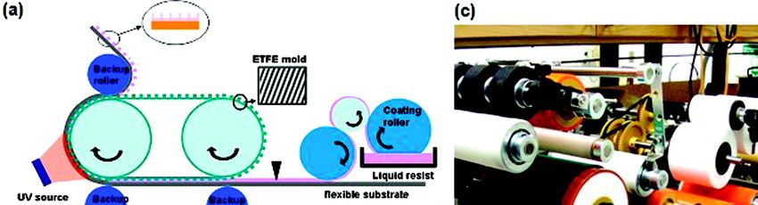
Appl. Sci. 2019, 9, 1206                                                                          2 of 15

researchers to establish programs in the field. Setting the display applications aside, since the early
2000s, micro-LEDs have been investigated to improve the luminescence efficiency for high-intensity
lighting motivated by their relatively high light extraction efficiency, better current spreading, and
lower self-heating effect [15–18]. In recent years, tens of companies around the world have been
involved in the micro-LED technology. For instance, Sony demonstrated its first 55" full-HD micro-LED
TV panel in 2012, which featured six million micro-LEDs. Compared with the existing Sony LCD and
plasma displays, the micro-LED prototype features 3.5 times higher contrast ratio, 1.4 times wider
color gamut, and 10 times faster response time. In 2018, Sony released its micro-LED crystal-LED
“CLEDIS” integrated display with micro-LED chip size of 0.003 mm2 , which has a contrast ratio of
over 1,000,000:1 and a black surface area of over 99%. CEA-Leti, a technology research institute in
France, demonstrated its prototype wide video graphic array (WVGA) micro-display with 10 µm
pixel pitch in 2017, which is based on the patterning of monochrome (blue or green) GaN micro-LED
arrays and hybridizing with complementary metal-oxide-semiconductor (CMOS) circuit. In 2018,
PlayNitride demonstrated two full-color micro-LED prototypes, one is a 0.89 inch 64 × 64 panel with
105 pixel per inch (PPI) resolution, and another is a 3.12 inch 256 × 256 panel with 116 PPI resolution.
AU Optronics Corp. has demonstrated 12.1 inch full-color micro-LED display with a 169 PPI and
1920 × 720 resolution achieved by micro-LEDs with pixel size less than 30 microns. X-Celeprint
has demonstrated both passive and active matrix full-color micro-LED displays. In 2018, a 5.1 inch
full-color micro LED display with active-matrix switching, which was made of 8 × 15 micron red,
green, and blue LEDs with a 70 PPI was presented. However, high volume commercialization of
micro-LED displays has not yet been reported.
      While the science is clear, new technical challenges arise when the chip size shrinks and chip
density expands. To conquer the related challenges, new techniques have been developing from
the ongoing investigations. There are a few recent review papers that have addressed the status
of micro-LED landscape, but have not sufficiently addressed the technological developments [1,19].
In this article, we overview the techniques in the key areas including mass transfer, monolithic
fabrication, and full-color realization. Current bottlenecks and likelihood of overcoming them are
also discussed.

2. Epitaxy and Chip Processing
     The main requirements on the epitaxial growth aspects of GaN-based micro-LEDs are the
wavelength and drive current homogeneity across the wafer and low defect density. Both Aixtron and
Veeco, two major manufacturers of deposition systems, have articulated their approaches to address
the particular needs for epitaxy of micro-LEDs [20,21]. Aixtron’s Planetary Reactor®technology uses
Gas Foil Rotation®for each wafer disks to enable uniform growth across an individual wafer and a
second rotation to improve wafer-to-wafer uniformity [20]. By incorporating a Cl2 in situ cleaning
process between each run and cassette-to-cassette wafer automation, a density of defects (with a
size larger than 1 µm) as low as ~0.1 defects/cm2 has been achieved. Veeco’s vertical-rotating disc
TurboDisc™ technology provides high 14 × 6” capacity with low defectivity and high uniformity [21].
A defectivity yield (percentage of killer defect number ≤ 1 per Epi donor field) above 90% has been
demonstrated for applications in smartphones and TVs, respectively.
     Desire for large diameter sapphire substrates to meet the needs of large-sized monolithic
micro-displays brings about some difficulties due to increased bowing induced by the large thermal
and lattice mismatches with the LED epilayer structure [22,23]. The primary problem associated with
wafer bowing is non-uniformity of the wafer surface temperature resulting in the spatially non-uniform
distribution of the indium molar fractions in the InGaN/GaN MQWs over the wafer. A temperature
non-uniformity of 1 ◦ C could induce a wavelength variation of 1.8 and 2.5 nm in blue and green LEDs,
respectively [24]. Wafer bowing also causes issues during the device fabrication process, such as wafer
cracking and degradation of device homogeneity in dry etching and other like processes. To deal with
these challenges, thicker substrates, optimized wafer holder designs, control of the coalescence stage,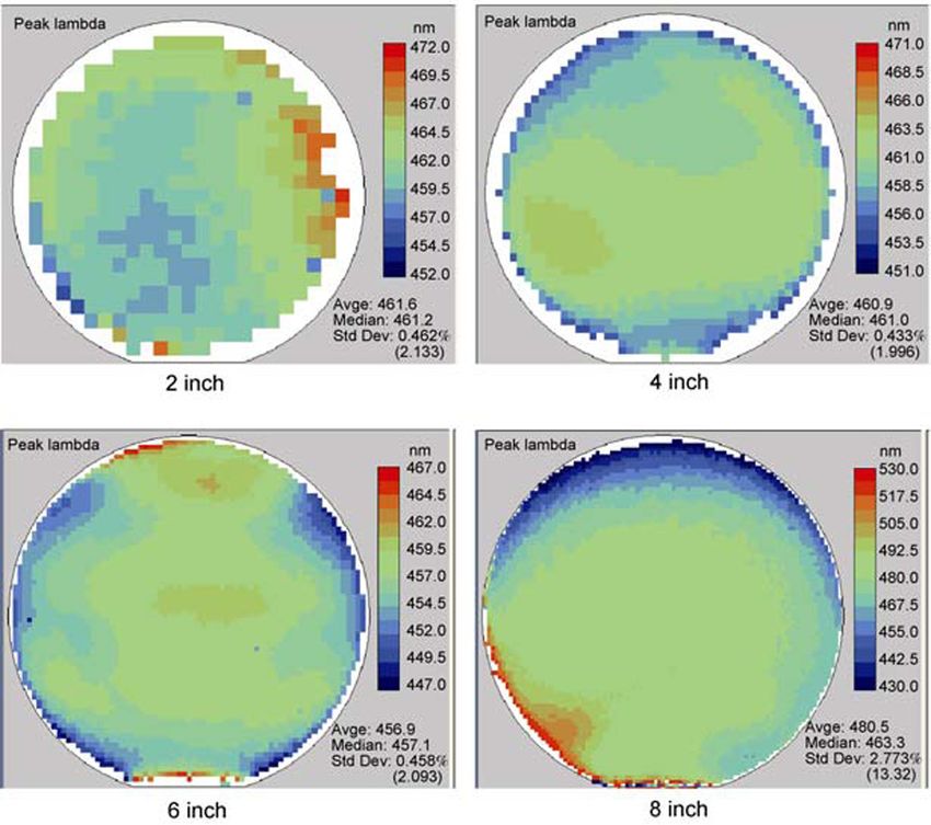
Appl. Sci. 2019, 9, 1206 3 of 15
insertion of strain-compensation
that photoluminescence (PL) peak layers, and internally
wavelength focused
uniformity laser 2treatment,
of about have been
nm in standard employed
deviation can
and or investigated [23–27]. For example, Lu et al. have shown that photoluminescence
be obtained in 2, 4, and 6 inch wafers by using proper wafer pocket design, except for the eight inch (PL) peak
wavelength uniformity
wafer, for which of about
the pocket 2 nmneeds
design in standard deviation can
to be improved, be obtained
as shown in 2, 4,
in Figure 1. and 6 inch wafers
In another study,
by
Aidausing proper
et al. have wafer
achievedpocket design,ofexcept
reduction for the in
the bowing eight inch
both wafer, for which
GaN-on-sapphire theGaN-on-silicon
and pocket design
needs to beby
substrates improved, as shown in Figure
stress implantation using 1.anIninternally
another study, Aida
focused et al.processing
laser have achieved[27]. reduction
Due to theof
the bowing
opposite in bothdirection,
bowing GaN-on-sapphire and GaN-on-silicon
laser-induced substrates
stress was implanted by stress
near implantation
the backside using
surface an
of the
internally focused laser
sapphire substrate processing [27].
to compensate Due
for the to the
strain opposite by
generated bowing direction, laser-induced
the GaN/sapphire stress
system, while it was
implanted nearnear the
the backside
interface surface
between ofthe
theGaN
sapphire
and substrate
silicon to to compensate
reduce the bowfor ofthe
thestrain generated
GaN-on-silicon
by the GaN/sapphire system, while it was implanted near the interface between the GaN and silicon
substrate.
to reduce the bow of the GaN-on-silicon substrate.
Figure 1. PL peak wavelength uniformity map for 2, 4, 6, and 8 inch wafers
wafers with
with zero
zero edge
edge exclusion.
exclusion.
Their PL uniformity is very comparable, all around 2 nm in standard deviation except the eight inch
wafer
wafer due
duetotonon-optimized wafer
non-optimized pocket
wafer design
pocket [23]. [23].
design Reprinted by permission
Reprinted from Springer
by permission Nature,
from Springer
Copyright (2011). (2011).
Nature, Copyright
Uniformity
Uniformity in in LED
LED pixel
pixel electrical
electrical parameters
parameters suchsuch asas forward
forward current-voltage
current-voltage characteristics
characteristics is is
also
also a very important factor for high quality displays. Optimized driving circuits, n- and
a very important factor for high quality displays. Optimized driving circuits, n- and p-electrode
p-electrode
structures,
structures, andandoptical
optical designs
designshave beenbeen
have developed to minimize,
developed if not totally
to minimize, if not eliminate, any electrical
totally eliminate, any
non-uniformity [28]. For example, in micro-LED arrays with a shared
electrical non-uniformity [28]. For example, in micro-LED arrays with a shared common n-electrodecommon n-electrode and
individually
and individually addressable p-electrodes,
addressable non-uniform
p-electrodes, operating
non-uniform currents
operating at the same
currents at theapplied voltage
same applied
for each for
voltage micro-LED occurs due
each micro-LED to variation
occurs in series resistances
due to variation arising from
in series resistances different
arising from distances
different
between the common n-electrode and the respective micro-LEDs [29].
distances between the common n-electrode and the respective micro-LEDs [29]. To minimize To minimize series-resistance
difference arisingdifference
series-resistance from varying conductive
arising from varyingpaths,conductive
a configuration
paths,using a common using
a configuration p-electrode with
a common
individually
p-electrode with addressable n-electrodes
individually has been
addressable developed,
n-electrodes haswhich
been mitigates
developed, thewhich
problem somewhat
mitigates the
as the conduction through n-GaN is less resistive. Such a reversed electrode
problem somewhat as the conduction through n-GaN is less resistive. Such a reversed electrode structure also makes
the array compatible
structure also makes withthe an n-type
array metal-oxide-semiconductor
compatible with an n-type transistor-based CMOS driver for
metal-oxide-semiconductor
faster modulation.
transistor-based CMOS driver for faster modulation.
Reduction
Reduction in in the
the size
size of
of micro-LEDs
micro-LEDs and and spacing
spacing between
between devices
devices cancan cause
cause problems
problems in in chip
chip
processing
processing and and deteriorate
deteriorate LED LED performance.
performance. One One important
important problem
problem is is the
the degradation
degradation of of the
the
quantum efficiency and homogeneity due to sidewall effect related to high density
quantum efficiency and homogeneity due to sidewall effect related to high density of surface defects of surface defects
caused
caused during
during device
device processing, which leads
processing, which leads toto degraded
degraded electrical
electrical injection
injection inin the
the p-GaN
p-GaN [5,30].
[5,30].
Acting
Acting as asnon-radiative
non-radiativecenters,
centers,thethe
surface defects
surface on the
defects onsidewalls significantly
the sidewalls degradedegrade
significantly the internal
the
quantum efficiency of the micro-LEDs. A decrease in maximum external
internal quantum efficiency of the micro-LEDs. A decrease in maximum external quantum efficiency quantum efficiency (EQE)
from
(EQE)~10%
from to ~5%
~10% towith reduction
~5% with in chip
reduction size size
in chip fromfrom
above 500 500
above µmμm × 500 µm
× 500 μm μm×× 10
toto1010µm 10 µm
μm
has
has been reported for micro-LEDs, as shown in Figure 2 [31]. The effect of size-reduction on the
been reported for micro-LEDs, as shown in Figure 2 [31]. The effect of size-reduction on the
performances is more noticeable for smaller LEDs with larger perimeter-to-area ratios. For LEDs
with the smallest dimensions (below 5 μm), the peak quantum efficiency was reported to be below
Appl. Sci. 2019, 9, 1206 4 of 15
performances is more noticeable for smaller LEDs with larger perimeter-to-area ratios. For LEDs with
the smallest
10% or even dimensions (below processing
1% [19]. Therefore, 5 µm), the peak quantum
technologies to efficiency
minimize was reported
sidewall damageto be below
and avoid,10%if
or even
not 1%eliminate,
totally [19]. Therefore, processing
degradation technologies
of electrical to minimize
injection are needed. sidewall
Chen etdamage
al. haveand avoid,that
reported if not
in
totally eliminate,
pyramidal degradation
micro-LEDs, a SiO2 of electrical
leakage injection
current are needed.
confinement layerChen et al. have
can decrease the reported that in
reverse leakage
pyramidal
current by micro-LEDs,
two orders ofa magnitude,
SiO2 leakageand current confinement
the light output oflayer can decreasecan
the micro-LEDs thebereverse leakage
improved by
currentaveragely
115% by two orders of magnitude,
[32]. Wong and demonstrated
et al. have the light outputthat of the micro-LEDs
using can be
atomic-layer improved(ALD)
deposition by 115% of
averagely
SiO [32]. Wong
2 for sidewall et al. have
passivation, demonstrated
size-dependent thaton
factors using
peakatomic-layer deposition
EQE of micro-LEDs can(ALD) of SiO2
be minimized
for sidewall
[33]. passivation,
Enhancement size-dependent
in light extraction factors on peak EQE
and reduction in of micro-LEDs
leakage currentcancaused
be minimized
by surface[33].
Enhancement in
recombination andlight extraction
sidewall damageandledreduction
to an EQE in leakage current
of 33% for 20 μm caused by micro-LEDs
× 20 μm surface recombination
with ALD
and sidewallcompared
passivation, damage led toto24%
an EQE of 33%
without sidewall µm × 20 µm Be
for 20 passivation. micro-LEDs
changing withmesaALD passivation,
etching process
compared to
formation 24% without
between sidewall
p-contact passivation. Bepads
and hybridization changing
into amesa
softeretching
plasmaprocess formationp-contact
and changing between
p-contact
metal from and hybridization
Ni-based pads into
to Ag-based, a softer
Olivier etplasma
al. haveand changingthe
improved p-contact
EQE ofmetal10 μmfrom Ni-based
pixel pitch
to Ag-based, Olivier et al. have improved the EQE of 10 pixel pitch
micro-LEDs from 4.8% to 6.8%, and achieved a brightness of 10 cd/m² [5]. Hwang et al. have
µm 7 micro-LEDs from 4.8% to
6.8%, andthat
achieved a brightness 7 2
reported high EQEs may beof 10 cd/m when
maintained [5]. Hwang et al.the
decreasing have reported
chip that100
size from high
μmEQEs
× 100mayμm be
to
maintained
10 μm × 10 μm, when decreasing
with peak EQEs the of
chip size
48.6 from
and µm × 100 µm[30].
100 respectively
40.2%, to 10 µm × 10 µm, with peak EQEs
of 48.6 and 40.2%, respectively [30].
Figure2.2.Effect
Figure Effectof
ofsize-reduction
size-reduction on
on the
the maximum EQE of GaN-based
GaN-based micro-LEDs.
micro-LEDs.Data
Datacompiled
compiled
from reference [31]. from reference [31].
3. Assembly Technologies
Two different approaches have been utilized to assemble displays constructed from individual
3. Assemblydies.
micro-LED Technologies
The first one is based on mass transfer, i.e., the so called pick-and-place approach,
which includes
Two picking
different up each have
approaches individual micro-LED,
been utilized and precisely
to assemble positioning
displays it onto
constructed the individual
from backplane,
followed electrically connecting it to the driver IC. This approach allows realization
micro-LED dies. The first one is based on mass transfer, i.e., the so called pick-and-place approach, of LED displays
in which the active LED area occupies only a small portion of the total
which includes picking up each individual micro-LED, and precisely positioning it onto the area. It can be used for
building large-size
backplane, followeddisplays ranging
electrically from several
connecting it to theinches to tens
driver of inches
IC. This (suchallows
approach as TV, smartphones,
realization of
LED displays in which the active LED area occupies only a small portion of the totalthe
and tablets), which are referred to as direct-view displays [34]. Alternatively, to avoid complicated
area. It can be
pick-and-place mass transfer process, a variety of monolithic fabrication methods
used for building large-size displays ranging from several inches to tens of inches (such have been proposed
as TV,
in order to realize micro-LED displays. Due to the limitation in wafer size used for the
smartphones, and tablets), which are referred to as direct-view displays [34]. Alternatively, to avoid growth of LEDs,
the monolithic integration approach can only be used for building relatively small-size
the complicated pick-and-place mass transfer process, a variety of monolithic fabrication methods displays such
as near-to-eye
have projectors
been proposed and smart
in order watches,
to realize whichdisplays.
micro-LED are referred
Duetotoasthe
micro-LED
limitationmicro-displays [34].
in wafer size used
for the growth of LEDs, the monolithic integration approach can only be used for building relatively
3.1. Mass Transfer Technologies
small-size displays such as near-to-eye projectors and smart watches, which are referred to as
Traditional
micro-LED pick and place
micro-displays [34]. equipment via mechanical manipulation fails to transfer millions of
LED dies in a cost-effective manner. In recent years, many companies have devoted considerable effort
3.1. Mass Transfer Technologies
Traditional pick and place equipment via mechanical manipulation fails to transfer millions of
LED dies in a cost-effective manner. In recent years, many companies have devoted considerable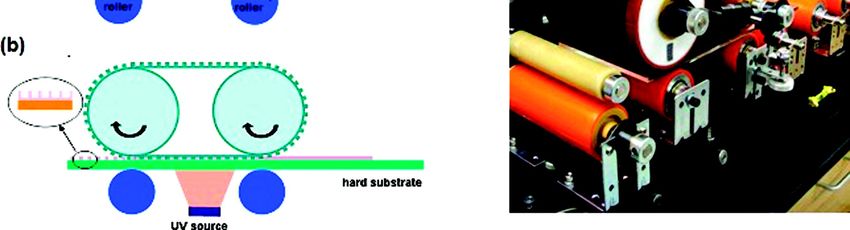
effort
Appl. Sci.to  overcome
           2019, 9, 1206 this problem by exploring a number of approaches involving of laser,     5 of 15
electrostatic, or electromagnetic, van der Waals forces, or fluidic forces, as summarized in Table 1.

to overcome this problem by exploring       a number
                                  Table 1. Some        of approaches
                                                mass transfer          involving of laser, electrostatic, or
                                                              technologies.
electromagnetic, van der Waals forces, or fluidic forces, as summarized in Table 1.
            Methods            Company/Institute            Force/means             Transfer rate
                                  Table 1. Some mass transfer technologies.      1,000 per shot/100
           Laser lift-off      Optovate/Uniqarta                 Laser
                                                                                  million per hour
         Methods          Company/Institute       Force/means
                                                            Gravity and         Transfer  rate
        Fluidic assembly         Foxconn(eLux)                                  50 million per hour
       Laser lift-off     Optovate/Uniqarta           Laser capillary1000 per shot/100 million per hour
    Fluidic  assemblyarray Foxconn(eLux)
       Electrostatic             Apple (LuxVue)Gravity and capillary
                                                            Electrostatic    50 million per
                                                                                     (Not   hour
                                                                                          found)
    Electrostatic array    Apple (LuxVue)          Electrostatic                 (Not found)
        elastomer stamp X-Celeprint
     elastomer stamp
                                   X-Celeprint van der Waals
                                                           van der Waals         1 million per hour
                                                                              1 million per hour
           Roll-to-roll
        Roll-to-roll           KIMM   KIMM         Roll stampRoll stamp            10,000
                                                                                10,000 per per
                                                                                           sec sec

      Laser-induced forward transfer is a mass transfer process which uses a laser beam to induce the
      Laser-induced forward transfer is a mass transfer process which uses a laser beam to induce the
separation of the micro-LEDs from their carrier substrate and then transfer them to a receive
separation of the micro-LEDs from their carrier substrate and then transfer them to a receive substrate,
substrate, as shown in Figure 3 [35]. The irradiation with a laser beam results in the light-matter
as shown in Figure 3 [35]. The irradiation with a laser beam results in the light-matter interaction at
interaction at the interface between the carrier substrate and the dies, with the result that the dies are
the interface between the carrier substrate and the dies, with the result that the dies are detached from
detached from the substrate and, at the same time, generates a local mechanical force to push the
the substrate and, at the same time, generates a local mechanical force to push the dies toward the
dies toward the receive substrate. The interfacial interaction can be the same as that used in laser
receive substrate. The interfacial interaction can be the same as that used in laser lift-off process of
lift-off process of GaN LEDs from the sapphire substrate, in which a thin GaN layer (~10 nm) is
GaN LEDs from the sapphire substrate, in which a thin GaN layer (~10 nm) is ablated at the substrate
ablated at the substrate epi interface and decomposed into nitrogen gas and liquid Ga. It may also be
epi interface and decomposed into nitrogen gas and liquid Ga. It may also be implemented via using a
implemented via using a temporary substrate with a polymer adhesive serving as the interfacial
temporary substrate with a polymer adhesive serving as the interfacial layer, which decomposes when
layer, which decomposes when irradiated with a laser beam. It has been reported that the
irradiated with a laser beam. It has been reported that the Laser-induced forward transfer technology
Laser-induced forward transfer technology enables some 1000 chips to be transferred per laser shot.
enables some 1000 chips to be transferred per laser shot. Optovate, a British optic tech company,
Optovate, a British optic tech company, has demonstrated its patterned laser lift-off (p-LLO) transfer
has demonstrated its patterned laser lift-off (p-LLO) transfer technology to transfer blue micro-LEDs
technology to transfer blue micro-LEDs from a sapphire wafer to a receive substrate. Val R. Marinov
from a sapphire wafer to a receive substrate. Val R. Marinov has reported that a transfer rate above
has reported that a transfer rate above 100 million per hour can be achieved using the massively
100 million per hour can be achieved using the massively parallel laser-enabled transfer (MPLET)
parallel laser-enabled transfer (MPLET) technology [36].
technology [36].

     Figure 3. Schematic of laser-induced forward transfer (LIFT) process. Adapted from reference [35],
      Figure 3. Schematic of laser-induced forward transfer (LIFT) process. Adapted from reference [35],
     Copyright 2016, with permission from Elsevier.
                                Copyright 2016, with permission from Elsevier.
      Fluidic assembly via gravity and capillary forces to drive and capture the micro-LEDs on
to theFluidic
        arrayassembly     via gravity
               of the driver    ICs hasand  capillary
                                          also        forces to drive
                                                been investigated     forand  capture
                                                                           mass        the micro-LEDs
                                                                                 transfer    of LED chips  on[37,38].
                                                                                                               to the
array  of the driveris ICs
The self-assembly             has also
                        conducted    in abeen  investigated
                                          fluid,               for mass acetone
                                                 such as isopropanol,      transfer or
                                                                                     ofdistilled
                                                                                         LED chips     [37,38].
                                                                                                   water.        The
                                                                                                          The fluid
self-assembly   is conducted     in a  fluid, such  as  isopropanol,     acetone  or  distilled
suspends and lets the LEDs move across the surface of the receive substrate till they reach the   water.  The   fluid
suspends   and lets
open receptor    sitesthe LEDsthey
                        where    moveareacross  the surface
                                          captured.   Once of    the receivethe
                                                              positioned,     substrate
                                                                                 anode andtill they reachelectrodes
                                                                                                cathode    the open
receptor  sites wherecan
of the micro-LEDs        theythen
                               are be
                                   captured.
                                       bondedOncewithpositioned,
                                                       the driver theICsanode    and cathode
                                                                           for electrical         electrodeseLux,
                                                                                           connections.       of thea
micro-LEDs     can    then   be   bonded    with   the   driver    ICs   for  electrical   connections.
Foxconn-owned company, has been developing its fluidic assembly methods for massive parallel                eLux,   a
Foxconn-owned      company,     has been   developing    its fluidic  assembly    methods     for massive
assembly of micro-LEDs [39]. It was reported that a fill (transfer) rate over 50 million devices per hour    parallel
can be achieved.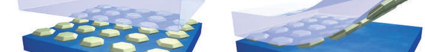
assembly of 9,
Appl. Sci. 2019, micro-LEDs
1206 [39]. It was reported that a fill (transfer) rate over 50 million devices6 per of 15
hour can be achieved.
LuxVue, an Apple Co.-owned company, has developed a transfer technology that operates in
LuxVue,
accordance withantheApple Co.-owned
electrostatic company,
principle, hasuses
which developed a transfer
the attraction technology
of opposite that operates
charges to pick up in
accordance with the electrostatic principle, which uses the attraction of opposite
micro-LEDs [40]. The process consists of picking up an array of micro-LEDs from a carrier substrate charges to pick up
micro-LEDs
with an array [40].
of The process consists
electrostatic transferofheads,
picking up anisarray
which of micro-LEDs
applied with a pull-infrom voltage
a carrierfrom
substrate
the
with an array of electrostatic transfer heads, which is applied with a pull-in
working circuitry to generate a grip pressure, contacting the micro-LEDs and transferring heat voltage from the working
from
circuitry
the head to andgenerate a grip
liquefying thepressure,
bondingcontacting the receive
layer on the micro-LEDs and transferring
substrate, and bonding heat
thefrom
array thetohead
the
and liquefying the bonding layer on the
receiving substrate and finally release the micro-LEDs. receive substrate, and bonding the array to the receiving
substrate and finally
X-Celeprint release the an
has developed micro-LEDs.
elastomer stamp micro-assembly technology for mass transfer of
X-Celeprint
micro-LEDs, has developed
as shown in Figure an 4elastomer
[41]. Thestamp
processmicro-assembly technology for
starts with preparation of mass transfer
a native wafer of
micro-LEDs, as shown in Figure 4 [41]. The process starts with preparation
substrate that supports the fully formed, organized arrays of micro-LEDs. Then a soft elastomeric of a native wafer substrate
that supports
stamp is brought the fully formed,with
into contact organized arrays of micro-LEDs.
the micro-LEDs. Then a soft
With a sufficiently highelastomeric
peel velocity,stamp theis
brought intoare
micro-LEDs contact with on
attached the to
micro-LEDs.
the stamp Withand alifted
sufficiently
away fromhigh peel velocity,
the native the micro-LEDs
substrate due to the are
attached on to the stamp and lifted away from the native substrate due to
rate-dependent adhesion forces, which are dominated by van der Waals interactions. Then, with athe rate-dependent adhesion
forces, which
sufficiently loware peel
dominated by van
velocity, the der Waals interactions.
micro-LEDs are releasedThen, withthe
from a sufficiently
stamp and lowpreferentially
peel velocity,
the micro-LEDs
adhered are released
to the receiving from the stamp and preferentially adhered to the receiving substrate.
substrate.
Figure4.
Figure Schematicillustration
4. Schematic illustrationofofthe
thegeneric
genericprocess
processflow
flowfor
forelastomer
elastomerstamp
stampmicro-assembly.
micro-assembly.(1) (1)
Prepare donor
Prepare donor substrate; apply rubber
rubber stamp;
stamp;(2)
(2)quickly
quicklypeel-back
peel-backstamp;
stamp;grab
grabobjects offoff
objects ofofdonor; (3)
donor;
apply inked stamp to receiving substrate; and (4) slowly peel-back stamp; print objects
(3) apply inked stamp to receiving substrate; and (4) slowly peel-back stamp; print objects onto onto receiver.
Reprinted/adapted
receiver. by permission
Reprinted/adapted from Springer
by permission Nature: Nature
from Springer Nature:materials, reference [41].
Nature materials, Copyright
reference [41].
(2009).
Copyright (2009).
Inanother
In anotherapproach,
approach,aaroll-to-plate
roll-to-platetransfer
transferprocess
processhas hasbeen
beendeveloped
developedby bythetheKorean
KoreanInstitute
Institute
of Machinery and Materials (KIMM) [42,43], which can be used to transfer micro-LEDs with aachip
of Machinery and Materials (KIMM) [42,43], which can be used to transfer micro-LEDs with chip
size and a chip thickness below 100 µm and 10 µm, respectively, as shown in
size and a chip thickness below 100 μm and 10 μm, respectively, as shown in Figure 5. The process Figure 5. The process
canprovide
can provideaatransfer
transferrate
rateof
ofup
uptoto10,000
10,000devices
devicesper persecond
secondfor forflexible,
flexible,stretchable
stretchableand andlightweight
lightweight
displays. The whole process consists of three roll transfer steps. The first step is
displays. The whole process consists of three roll transfer steps. The first step is to pick up and to pick up andplace
place
the array of control TFTs on to a temporary substrate by roll stamp coated with
the array of control TFTs on to a temporary substrate by roll stamp coated with disposable transfer disposable transfer
film. Then
film. Then in
in the
the second
secondstep,
step,micro-LEDs
micro-LEDsare arelifted offoff
lifted from their
from support
their supportsubstrate
substrateto betolocated onto
be located
the temporary substrate and connected with the TFTs by solder bonding. In the
onto the temporary substrate and connected with the TFTs by solder bonding. In the final step, the final step, the array of
the interconnected
array micro-LED+TFTs
of the interconnected is roll-transferred
micro-LED+TFTs onto a target
is roll-transferred ontosubstrate
a targetto substrate
form an active
to formmatrix
an
micro-LED display.
active matrix micro-LED display.
3.2. Monolithic Fabrication of Micro-Displays
Simply, the monolithic methods can be divided into two categories, i.e., fully monolithic
integration and monolithic hybrid. In conventional display technologies, such as LCDs or OLEDs,
the processing temperatures for the emission elements are typically below 400 ◦ C, which can be
withstood by the CMOS-based driver ICs. Therefore, fully monolithic integration via direct process
of emission elements on the driver ICs is not problematic. However, the growth temperatures of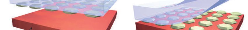
Appl. Sci. 2019, 9, 1206 7 of 15
III-nitride LEDs are typically above 900 ◦ C. It is impossible to grow and process LEDs directly on top
of backplane with conventional ICs. Additionally, some new fully monolithic methods have been
proposed and investigated.
Figure 5. Schematics of (a) roll-to-roll nanoimprint lithography (R2RNIL) and (b) roll-to-roll
nanoimprint lithography (R2PNIL) process. (c) Photograph of a six-inch-capable R2R/R2PNIL
apparatus [38]. Copyright 2009 American Chemical Society.
3.2. Monolithic Fabrication of Micro-Displays
Simply, the monolithic methods can be divided into two categories, i.e., fully monolithic
integration and monolithic hybrid. In conventional display technologies, such as LCDs or OLEDs,
the processing temperatures for the emission elements are typically below 400 °C, which can be
withstood by the CMOS-based driver ICs. Therefore, fully monolithic integration via direct process
of emission
Figure
Figure 5. 5.elements
Schematicson the
Schematics driver
ofof (a)
(a) ICs is nanoimprint
roll-to-roll
roll-to-roll not problematic.
nanoimprint However,
lithography
lithography the growth
(R2RNIL)
(R2RNIL) and
and (b)(b)temperatures
roll-to-roll of
roll-to-roll
III-nitride LEDs
nanoimprint are typically
nanoimprint lithography above 900 °C.
(R2PNIL) process.
lithography (R2PNIL) It is impossible
process. (c)(c) Photograph to
Photograph of grow and process
of aa six-inch-capableLEDs directly
six-inch-capable R2R/R2PNIL
R2R/R2PNIL on top
of backplane
apparatus with conventional
[38]. Copyright
Copyright ICs. Additionally,
2009 American some new fully monolithic methods have been
Chemical Society.
proposed and investigated.
Since
Since III-nitrides
3.2. Monolithic Fabrication
III-nitrides are
areofexcellent materials
materials for
Micro-Displays
excellent for both
both LEDs
LEDs and and high-frequency
high-frequency and and high-power
high-power
transistors,
transistors, fully
fully monolithic
monolithic active
active matrix
matrix micro-displays
micro-displays can
can be
be realized
realized by
by the
the integration
integration of
of
Simply, the monolithic methods can be divided into two categories, i.e., fully monolithic
individual
individual GaN-based
GaN-based LED
LED driven
driven by
by aa GaN-based
GaN-based transistor
transistor for
for each
each pixel.
pixel. Lau
Lau et
et al.
al. have reported
have reported
integration and monolithic hybrid. In conventional display technologies, such as LCDs or OLEDs,
monolithic
monolithic integration
integration of
of InGaN/GaN
InGaN/GaN light emitting
light emitting diodes
diodes (LEDs) with AlGaN/GaN heterojunction
the processing temperatures for the emission elements are(LEDs) withbelow
typically AlGaN/GaN
400 °C, heterojunction
which can be
field effect transistors
field effectbytransistors (HFETs)
(HFETs)driver [44]
[44] oror vertical metal-oxide-semiconductor field effect transistor
withstood the CMOS-based ICs.vertical
Therefore,metal-oxide-semiconductor
fully monolithic integration fieldvia effect
directtransistor
process
(VMOSFET)
(VMOSFET) drivers
drivers [45],
[45], by
by selective growth
selective growth of of HFET
HFET or or VMOSFET
VMOSFET structures
structures onon the
the LED
LED epilayers,
epilayers,
of emission elements on the driver ICs is not problematic. However, the growth temperatures of
as
as shown in
in Figure
shown LEDs Figure 6.
6. Alternatively,
Alternatively, lateral
lateral integration via viatoselective removal of the
the HFET structure
III-nitride are typically above 900 °C. Itintegration
is impossible selective
grow and removal
processofLEDs HFET
directlystructure
on top
followed by selective growth of the LED structure on top of the exposed GaN buffer layer [46] or
of backplane with conventional ICs. Additionally, some new fully monolithic methods have[46]
followed by selective growth of the LED structure on top of the exposed GaN buffer layer or
been
selective removal
selective and removal of the LED structure followed by selective growth
of the LED structure followed by selective growth of the of the metal-oxide-semiconductor
proposed investigated.
field effect transistor (MOSFET)
metal-oxide-semiconductor on toptransistor
field effect of the exposed n-GaN layerof [47] have also been layer
reported.
Since III-nitrides are excellent materials for (MOSFET)
both LEDson top
and the exposed
high-frequency n-GaN
and high-power[47]
Although
have also itbeen
has reported.
been demonstrated
Although that
it thebeen
has performance
demonstratedof the that
integrated
the single LED-transistor
performance of the chip is
integrated
transistors, fully monolithic active matrix micro-displays can be realized by the integration of
comparable to discrete LEDs
single LED-transistor and
chip driven transistors [44]
is comparable to fabrication
discrete of micro-LED
LEDs displays using this approach
individual GaN-based LED by a GaN-based transistor forand
eachtransistors
pixel. Lau et[44] fabrication
al. have reportedof
has not
micro-LED yet been reported.
displays using this approach has not yet been reported.
monolithic integration of InGaN/GaN light emitting diodes (LEDs) with AlGaN/GaN heterojunction
field effect transistors (HFETs) [44] or vertical metal-oxide-semiconductor field effect transistor
(VMOSFET) drivers [45], by selective growth of HFET or VMOSFET structures on the LED epilayers,
as shown in Figure 6. Alternatively, lateral integration via selective removal of the HFET structure
followed by selective growth of the LED structure on top of the exposed GaN buffer layer [46] or
selective removal of the LED structure followed by selective growth of the
metal-oxide-semiconductor field effect transistor (MOSFET) on top of the exposed n-GaN layer [47]
have also been reported. Although it has been demonstrated that the performance of the integrated
single LED-transistor chip is comparable to discrete LEDs and transistors [44] fabrication of
micro-LED displays using this approach has not yet been reported.
Figure 6. Optical micrograph of the monolithically integrated VMOSFET-LED device. Reprinted from
reference [45], with the permission of AIP Publishing.
Si-based TFT, instead of III-nitride-based transistor, has also been investigated for on-chip driving
III-nitride LEDs. Tsuchiyama et al. have reported monolithic integration of a Si n-MOSFET and a GaN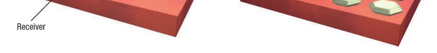
Appl. Sci. 2019, 9, 1206                                                                            8 of 15

micro-LED [48,49]. To achieve this, a Si layer from a silicon-on-insulator (SOI) substrate was bonded to
a GaN-based LED structure with a top SiO2 layer via surface-activated bonding [44]. Si-MOSFETs were
then fabricated on the Si/SiO2 /GaN-LED structure by using a CMOS process line. The interconnects
were realized via the connection of the cathode of a 30 × 30 µm2 sized GaN-LED to the drain of
a Si n-MOSFET with a gate width of 100 µm and gate length of 10 µm. It was found that thermal
degradation could be avoided by optimizing the thickness of the top-Si layer coupled with processing
below 900 ◦ C. It is stated that electrical and optical properties of the integrated Si n-MOSFET and GaN
micro-LED devices are comparable to those of the standard devices.
     Due to the difficulties and incompatibility between the micro-LED and driver IC processes in
fully monolithic integration, the most common approach adopted by micro-LED display developers
is monolithic hybrid. This approach comprises fabrication of III-nitride based micro-LED arrays,
manufacturing of Si-based CMOS driver matrix, and then their hybrid integration in order to allow
control of the LED pixels individually. The hybridization process is generally based on the flip-chip
bonding technology, which has been widely developed in III-V/Si photonics for high-performance
switching and computing [50]. For example, by using 6 µm-sized indium metal bumps deposited
on micro-LED pixels as bonders, Day et al. have demonstrated fabrication of a 160 × 120 VGA
micro-display with a pixel pitch of 15 µm [51].
     To further shrink the pixel pitch down to below 10 µm for higher resolution, CEA-Leti has
developed a micro-tube technology to perform the integration process [52,53]. The key step to the
interconnection is the insertion of gold capped micro-tubes on the pads of Si circuit into the soft indium
pads on the micro-LED array, with the micro-tubes created by using conformal metal deposition and
“gap fill” type processes. Blue and green active-matrix LED micro-displays with a 10 µm pixel pitch and
a resolution of 873 × 500 using 6 µm-sized micro-LEDs have been demonstrated via this technology.
     In addition to the abovementioned monolithic fabrication approaches, it has also been
demonstrated that micro-LEDs displays can be built by using GaN-based nanowire LEDs, without the
need of mass transfer. Prototypes including a 1.5” 264 PPI RGB wearable display using 20 µm-sized
micro-LEDs on a LTPS glass backplane, and a 0.7” 1000 PPI RGB display using 10 µm-sized micro-LEDs
on a CMOS backplane have been unveiled by glō-USA, in which direct wafer-to-wafer transfer
technology was employed.

4. Full-Color Schemes
      As for most micro-display applications, full-colors (composed of the three primary colors red,
green, and blue) are needed for each pixel. The widespread display technology LCD is based on light
generated by an LED backlight and passing through a matrix of liquid crystal “light switches” and
color filters constituting the individual subpixel. While micro-LED display is based on a matrix of tiny
light emitters made of micro-LEDs for each subpixel in which brightness can be individually controlled.
However, III-nitride LEDs, similar to other heterojunction-based semiconductor structures, are nearly
monochromatic emission sources, emitting light at a single color, with its wavelength determined
mainly by the indium content in the InGaN/GaN multiple quantum wells (MQWs). Although several
approaches exist to produce full-color micro-displays from single color micro-LEDs, it remains to be a
challenge for developers.
      The most straightforward approach for full color is to assemble discrete commercial LEDs with
the three different colors to form an array, with each pixel containing red, green, and blue LED dies.
In theory, InGaN/GaN MQWs LEDs can generate all these three colors by tuning the indium content in
the MQWs. Unfortunately, InGaN-based green and red LEDs still possess a relatively low luminescence
efficiency, which partially results from large lattice mismatch between the InGaN active layer and GaN
buffer for green and red wavelengths. This limits the progress in developing full-color displays using
GaN family alone. GaP/GaAs based LEDs can be used to emit red light, but may suffer from even
more significant drop in EQE as the size shrinks [30].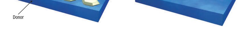
Appl. Sci. 2019, 9, 1206                                                                           9 of 15

      To enhance the color quality, Soitec, a French company, has developed a substrate technology
called InGaNOX [54,55]. The initially strained 200 nm thick InGaN layer with indium content from
1.5% to 8% is grown on a GaN/sapphire substrate. Then the thin InGaN layer is transferred using
Soitec’s Smart Cut™ technology onto a compliant layer deposited on a substrate. After patterning,
the strain-relaxed, Ga-face-exposed InGaN layer with an in-plane lattice parameter ranging from 3.190
to 3.205 Å is transferred to a final handle substrate with sizes up to 300 mm, which can be sapphire,
glass, or silicon. By using this technology, InGaN micro-LEDs with full-color emission (without using
phosphor conversion) grown on the same wafer have been fabricated. Red LEDs with emission
wavelength up to 630 nm and a chip size of 100 × 100 µm2 have been demonstrated by Soitec.
      Another approach utilizes single color micro-LED array but with color converters. The color
of the pump LEDs in the LED arrays can be blue or ultraviolet (UV), and phosphors or quantum
dots (QDs) can be employed as color converters. When blue micro-LED pump is used, only red and
green color-converters are needed with blue partially getting through; while the employment of UV
micro-LEDs requires blue, red, and green color-converters. One major challenge in obtaining full-color
with this method is the precise placement of the color-convertors on to the sub-pixels with a very
small size. A variety of technologies can be used to deposit color converters for LED color-conversion,
including spin coating, mist coating, pulse-spray coating, stamp printing, ink jet printing, and aerosol
jet printing [56–59]. Among all of these technologies, aerosol jet printing has the advantages of being
precise, non-contact, masks-less, and capable of depositing highly viscous inks and depositing more
materials in one printing step. Therefore, this method is deemed as a suitable approach for application
in color-conversion in high-resolution micro-LED displays.
      Phosphors, which are typically micrometer-sized powders, have the advantages of high quantum
yield (exceeding 80%), high thermal stability (with temperature up to 150 ◦ C), high chemical stability
(moisture resistance), and stable quantum yield and spectral properties under continuous irradiation
with high light flux and fast luminescence decay. Consequently, they are widely used in white LEDs
for general lighting [60–62]. The shortcomings, however, are strong light scattering and poor beam
collimation due to their large size [61]. These shortcomings lead to low color uniformity which becomes
more pronounced for micro-LED displays in which the phosphor size is comparable to that of small
micro-LEDs. Reducing the phosphor size down to the nanometer scale has the potential to enhance
luminance homogeneity due to reduced light scattering [63]. However, it also results in a reduction in
quantum efficiency.
      QDs have been proposed as an alternative method for full-color micro-LED displays due to their
excellent properties, which include high quantum efficiency, large absorption cross-section, and tunable
emission wavelength [62]. As compared to typical phosphor particles, the size of colloidal QDs lies in
the range of nanometers. Therefore, enhanced color uniformity via QDs-based color-conversion can be
expected. White light generation and good luminous efficacy of radiation have been demonstrated in
128 × 128 full-color micro-LED arrays with a pixel pitch of 40 µm, by combining UV micro-LEDs with
RGB CdSe QDs deposited via aerosol jet printing [56]. For commercialization, some critical factors in
QDs, such as photo-stability and thermal quenching, would have to be addressed.
      To ensure the color purity and contrast ratio, the optical cross-talk effect resulting from the
inaccurate distribution of color converters must be minimized. It has been reported that for a 128 ×
128 micro-LED array with 35 µm × 35 µm pixel size, cross-talk resulting from the overflow of QDs
during solvent evaporation still caused color shift, even though the aerosol jet printing technique
with optimized parameters was employed [64]. To reduce cross talk, Lin et al. have developed a
lithographically fabricated photoresist mold consisting of a window for QD jetting and a light blocking
wall, as shown in Figure 7 [64]. Using the window-confined photoresist mold led to successful
suppression of the overflow of the QDs resulting in a clear boundary between the pixels. With silver
coatings on the sidewall of the mold, light leakage was also prevented and, hence, a near zero cross-talk
was achieved. In order to increase the utilization of light from UV micro-LED array, and avoid biological
damage, a distributed Bragg reflector (DBR) structure has been implemented on the QDs-deposited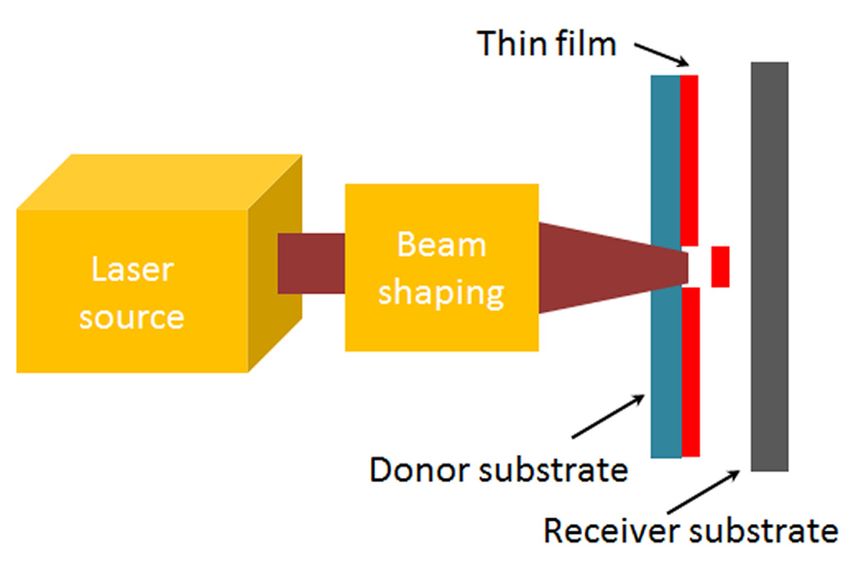
Appl. Sci. 2019, 9, 1206 10 of 15
and avoid biological damage, a distributed Bragg reflector (DBR) structure has been implemented
on the QDs-deposited LED array, which enhanced the QD emission intensity by 23%, 32%, and 5%
LED
for array,
red, which
green, andenhanced the QD emission
blue, respectively [64]. intensity by 23%, 32%, and 5% for red, green, and blue,
respectively [64].
Figure
Figure 7.
7. Process
Processflow
flowofofa full-color
a full-colormicrodisplay.
microdisplay.(a)(a)
TheThe
structure of the
structure micro-LED
of the arrays.
micro-LED (b)
arrays.
Aligning the mold to the UV micro-LED array. (c–e) Consequently jetting the RGB
(b) Aligning the mold to the UV micro-LED array. (c–e) Consequently jetting the RGB QDs insideQDs inside the
mold window
the mold windowto form
to formthethe
full-color pixels.
full-color Reprinted
pixels. Reprintedfrom
fromreference
reference[64],
[64],with
withthe
the permission
permission of
Chinese Laser Press.
In another study, Chen et al. have used three strategies to improve pixel contrast ratio and color
purity of monolithic
monolithic RGB RGB micro-LEDs
micro-LEDsbased basedon onblue
blueLEDs
LEDsand andredredand
andgreen
greenQDs,
QDs,which
whichinclude
includea
a black
black matrix
matrix photoresist
photoresist with
with light-blocking
light-blocking capability
capability to to block
block light
light leakage
leakage from
from thethe sidewalls,
sidewalls, a
a DBRwith
DBR withhigh
highreflectivity
reflectivityatatblue
bluelight
lighton
onthe
thetop
top of
of red
red and green QDs/micro-LEDs
QDs/micro-LEDs and and a hybrid
Bragg reflector (HBR) structure on the bottom for multiple reflection of the blue light into the color
conversion layer
layer [65].
[65]. Consequently,
Consequently,the thecontrast
contrastratio
ratioofofthe
themicro-LEDs
micro-LEDs was
was improved
improved from 11 to
from 11 22,
to
and the red and green light output intensities of the micro LEDs were enhanced
22, and the red and green light output intensities of the micro LEDs were enhanced by about 27%. by about 27%.
To improve
improvelight lightefficiency andand
efficiency eliminate color color
eliminate crosstalk of color-converted
crosstalk micro-LED
of color-converted displays,
micro-LED
Gou et al. Gou
displays, haveetproposed
al. havea proposed
funnel-tube array designarray
a funnel-tube in color-converted micro-LED displays
design in color-converted with
micro-LED
color filter
displays [66].
with Based
color on[66].
filter device
Based simulation
on device and modeling,
simulation it was
and founditthat
modeling, wasby usingthat
found funnel-tube
by using
array to confine
funnel-tube arrayphosphors
to confineinside each subpixel,
phosphors inside each thesubpixel,
optical efficiency
the opticalofefficiency
the micro-LEDof the display
micro-LEDcan
be improved
display can beby ~3 times,
improved bywhile
~3 times,the while
crosstalk is eliminated.
the crosstalk With optimized
is eliminated. tapper tapper
With optimized angle of the
angle
funnel-tube,
of the ambient
the funnel-tube, contrast
the ambient ratio can
contrast also
ratio canbealso
improved due to due
be improved higher light intensity.
to higher light intensity.
5. Current
5. Current Challenges
Challenges and
and Prospects
Prospects
Despite the
Despite the above-discussed
above-discussed technological
technological advancements,
advancements, there there are
are still
still some
some remaining
remaining critical
critical
bottlenecks which
bottlenecks whichneed
needtotobebeovercome
overcome forfor
highhigh volume
volume manufacturing
manufacturing of micro-LED
of micro-LED displays.
displays. The
The major one is the pixel yield of the display. To control the dead pixel number
major one is the pixel yield of the display. To control the dead pixel number less than 5 in an RGB less than 5 in an RGB
full-color full
full-color full high
high definition
definition (FHD)
(FHD) display (1920 ×
display (1920 1080 pixels),
× 1080 pixels), the
the yield
yield should
should be be 99.9999%,
99.9999%, which
which
is too
is too high
high for
for today’s
today’s achievable
achievable level.
level. AA dead
dead pixel
pixel can
can appear
appear at at different
different stages
stages ofof the
the fabrication,
fabrication,
such as epitaxy, LED chip process, transfer process. For example, in the
such as epitaxy, LED chip process, transfer process. For example, in the case of monolithic case of monolithic fabrication,
in a passive-matrix
fabrication, micro-LED array
in a passive-matrix fabricatedarray
micro-LED by flip-chip bonding
fabricated of a GaN bonding
by flip-chip micro-LED of array
a GaN on
a silicon submount with common p-electrode stripes, numerous dead pixels
micro-LED array on a silicon submount with common p-electrode stripes, numerous dead pixels are are formed because of
physical disconnection from the p-electrode line caused by severe bonding
formed because of physical disconnection from the p-electrode line caused by severe bonding failures [67]. As another
example,[67].
failures the As
photoresist
another residue
example, inside the gaps between
the photoresist residuethe LEDthe
inside elements can greatly
gaps between the undermine
LED elements the
yield of the display [29]. Without adding an O -based plasma ashing step, for
can greatly undermine the yield of the display2[29]. Without adding an O2-based plasma ashing step, the arrays with 170 µm
gapsthe
for between
arraysmesas, the micro-LED
with 170 μm gaps betweenelement yield
mesas, in the
thearray is approximately
micro-LED element yield90%. However,
in the arraywhen is
the gap width is90%.
approximately reduced to 6 µm,
However, when the the
yield
gapdrops
width to around
is reduced67%.to Introduction
6 μm, the yield of the ashing
drops step to
to aroundAppl. Sci. 2019, 9, 1206 11 of 15
67%. Introduction of the ashing step to remove the photoresist residues improved the yield to 100%
and over 95% for the 170 μm and 6 μm gap arrays, respectively.
remove the photoresist
Another challengeresidues improved
is the defect the yield to
management and100% andtechnology.
repair over 95% forFor thea170zero and 6defect
µmdead µm
gap arrays, respectively.
display, even assuming an extremely high yield, a repair process is unavoidable. A straightforward
Another
solution is tochallenge
increase the is the defect management
redundancy by doubling andthe
repair technology.
number For a zero
of micro-LED dead defect
element display,
for each pixel.
even assuming an extremely high yield, a repair process is unavoidable.
However, the effectiveness of the built-in redundancy depends on the initial defectivity yield. If the A straightforward solution is
toyield
increase the redundancy by doubling the number of micro-LED element
is 99.99%, doubling the number of micro-LED can reduce the number of dead pixels from 5000 for each pixel. However, the
effectiveness
to five pixelsofin theanbuilt-in redundancy
FHD display. depends
However, on the
if the initial
yield defectivity
is only 99.9%, yield. If the yield
the number is 99.99%,
of dead pixels
doubling the number of micro-LED can reduce the number of
would be still 500 [68]. Since doubled, number-wise, micro-LEDs are used, the cost of the dead pixels from 5000 to five pixels in
display
an FHD be
would display.
greatly However,
increased. if the yield is onlysome
Alternatively, 99.9%,developers
the numberhave of dead pixels individual
proposed would be still 500repair
pixel [68].
Since doubled, number-wise, micro-LEDs are used, the cost of the
technologies. Unfortunately, this approach is also costly, and cannot be applied for displays display would be greatly increased.
Alternatively, some developers
produced by monolithic have proposed individual pixel repair technologies. Unfortunately,
fabrication.
this approach
The cost is also costly,
remains to beand cannot be obstacle.
a formidable applied forThedisplays
success produced
of micro-LED by monolithic fabrication.
display insertion hinges
The cost remains to be a formidable obstacle. The success of micro-LED
on its cost competitiveness against the competing technologies such as the conventional LCD/OLED display insertion hinges
on its cost but
displays, competitiveness
at the time ofagainst the competing
this writing technologies
cost competiveness such
is not asrealistic.
yet the conventional
The cost of LCD/OLED
micro-LED
displays, but at the time of this writing cost competiveness is not yet
displays naturally encompasses wafer and chip processing cost, repair cost, post-processing cost, realistic. The cost of micro-LED
displays naturally
and transfer cost in encompasses wafer and chip approach
the case of pick-and-place processing[69].cost,Figure
repair8cost,
shows post-processing
the calculatedcost, LEDandand
transfer cost in the
mass transfer costcase of pick-and-place
versus micro-LED size approach [69]. 2560
for a 5.8” Figure × 81440
shows the calculated
resolution quad highLED and mass
definition
transfer
(QHD) cost versus micro-LED
smartphone display andsize 3840for× a2160 2560 × 1440
5.8”resolution 4K resolution
TV displayquad by IHS high definition
Research and(QHD)
Veeco
smartphone and 3840 ×
[21]. Based on the assumption of $400 per 6” processed epitaxy wafer and a LED gap of 2 μm,Based
display 2160 resolution 4K TV display by IHS Research and Veeco [21]. a size
on the assumption of $400 per 6” processed epitaxy wafer and
of 3 μm × 3 μm and 9 μm × 9 μm is needed for smartphone and TV, respectively, to meet the a LED gap of 2 µm, a size of 3 µm ×
3competitive
µm and 9 µm × 9 µm is needed for smartphone and TV, respectively,
cost targets with OLED. Continual technology advancements can be expected to to meet the competitive cost
targets
provide with
theOLED.
pathways Continual
to realize technology advancements
the cost expectation, butcanmorebe expected to provide
time is needed to bethein apathways
position to
for
realize the cost expectation, but more time is needed to be in a position
us to select which of the strategies touched upon in this paper would get the technology of choice for us to select which of the
strategies
where it needstouched upon in this paper would get the technology of choice where it needs to be.
to be.
Figure 8. LED and mass transfer costs versus micro-LED size for 5.8” QHD smartphone (a) and 55” 4K
Figure
TV (b) by8.IHS
LEDResearch
and mass transfer
and Veeco costs versus micro-LED
[21]. Courtesy of Dr. Ajitsize for 5.8”
Paranjpe of QHD
Veeco smartphone
Instruments,(a) and 55”
Inc.
4K TV (b) by IHS Research and Veeco [21]. Courtesy of Dr. Ajit Paranjpe of Veeco Instruments, Inc.You can also read