Plasmonic nano-architectures for surface enhanced Raman scattering: a review
←
→
Page content transcription
If your browser does not render page correctly, please read the page content below
Plasmonic nano-architectures for
                surface enhanced Raman scattering: a
                review

                G. V. Pavan Kumar

Downloaded From: https://www.spiedigitallibrary.org/journals/Journal-of-Nanophotonics on 18 Nov 2020
Terms of Use: https://www.spiedigitallibrary.org/terms-of-use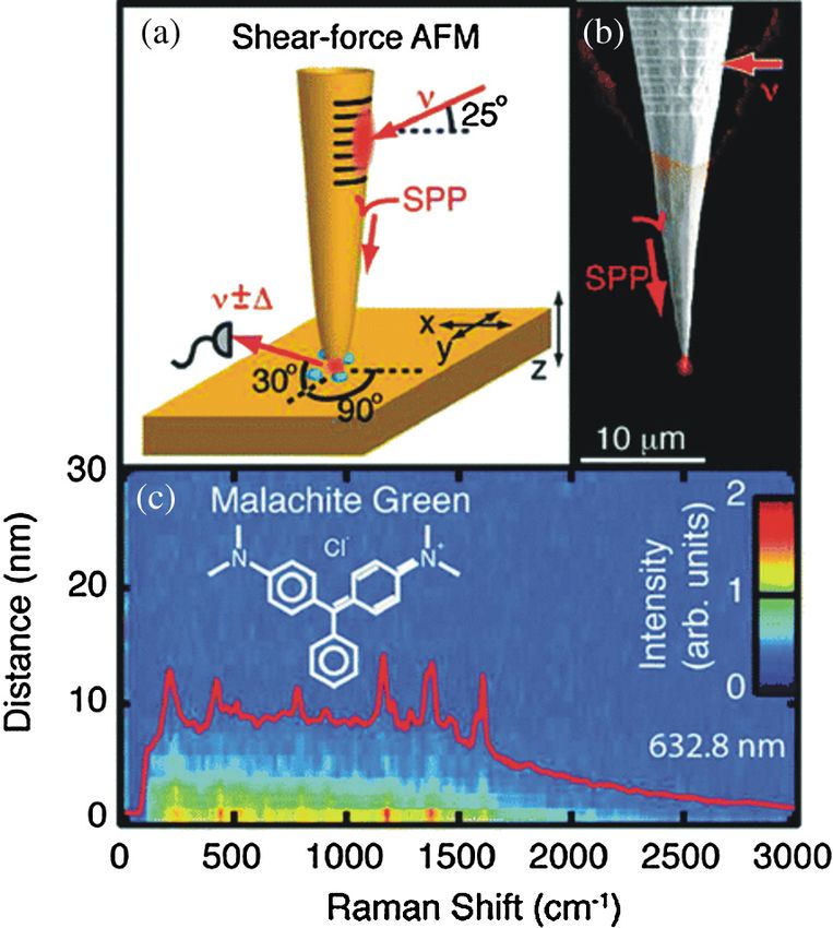
Plasmonic nano-architectures for surface enhanced
                                                Raman scattering: a review

                                                                           G. V. Pavan Kumar
                                 Indian Institute of Science Education and Research (IISER), Division of Physics and Chemistry,
                                                Photonics and Optical Nanoscopy Laboratory, Pune 411008, India
                                                                      pavan@iiserpune.ac.in

                                 Abstract. Surface enhanced Raman scattering (SERS) is an optical spectroscopy technique with
                                 single molecule sensitivity and chemical specificity. The electromagnetic enhancement mechan-
                                 ism of SERS is facilitated by the localized surface plasmons of metallic nanostructures utilized in
                                 experiments. The magnitude of the local optical field created by the plasmonic nanostructure
                                 depends on parameters such as size, shape, morphology, arrangement, and local environment of
                                 the nanostructure. By tuning these parameters, electromagnetic hot spots can be created to facil-
                                 itate ultra-sensitive, subwavelength SERS detection platforms. In recent years, there have been a
                                 number of innovations in nanofabrication and synthesis of plasmonic nanostructures. This has
                                 led to a variety of plasmonic nano-architectures that can be harnessed for SERS. Recently inves-
                                 tigated plasmonic nanostructures in the context of SERS include nanosphere dimers, individual
                                 nanocubes, nanotriangular arrays, nano-pyramid shells, individual and assembly of nanorods,
                                 nanowires, and nanotips, and some unconventional nano-architectures. Challenges in fundamen-
                                 tal and application aspects of SERS remain for future research. © 2012 Society of Photo-Optical
                                 Instrumentation Engineers (SPIE). [DOI: 10.1117/1.JNP.6.064503]
                                 Keywords: surface enhanced Raman scattering; plasmonics; nano-optics; spectroscopy.
                                 Paper 12011V received Feb. 6, 2012; revised manuscript received Mar. 16, 2012; accepted for
                                 publication Mar. 19, 2012; published online May 4, 2012.

                                 1 Introduction
                                 One of the most important aspects of nanoscale materials is that many of its physical properties
                                 can be dramatically tuned by altering its size, shape, and morphology. In recent years, various
                                 new tools and techniques have emerged to fabricate and visualize nanomaterials.1 This has led to
                                 better understanding of physical and chemical properties of nanomaterials, and has further moti-
                                 vated research in various directions. The preparation of nanostructures can be broadly classified
                                 in to two categories: the top-down approach and the bottom-up approach. In the top-down
                                 approach, such as electron beam lithography,2 the starting point is a bulk material which is
                                 further processed by the electron beam to create nanoscale entities. In contrast, the bottom-
                                 up approach, such as chemical synthesis or self assembly,3 starts with molecular entities and
                                 builds up the nanomaterials. Each approach has its advantages and shortcomings, but can
                                 also be combined to prepare nanomaterials with unique properties.4,5
                                     Of the many kinds of nanomaterials, metal nanostructures have been extensively studied in
                                 the context of their optical properties.6 The interaction of light with noble metals, such as silver,
                                 gold, and copper, has been a topic of research for number of years,6,7 but in last couple of decades
                                 there is a surge of interest8–10 in understanding how light interacts with metallic nanostructures.
                                 One of the main reasons for this is the plasmonic property of metallic nanostructures in and
                                 around the visible frequency spectrum. Plasmons are essentially the coupled oscillations of
                                 light and free electrons at the metal-dielectric interface. These coupled oscillations facilitate opti-
                                 cal fields that can be used for propagation and localization of light beyond the diffraction limit. In
                                 the context of plasmons there are two fundamental excitations: surface plasmon polaritons
                                 (SPPs) and localized surface plasmons (LSPs). SPPs are propagating plasmons and can be

                                 0091-3286/2012/$25.00 © 2012 SPIE

                                 Journal of Nanophotonics                              064503-1                             Vol. 6, 2012

Downloaded From: https://www.spiedigitallibrary.org/journals/Journal-of-Nanophotonics on 18 Nov 2020
Terms of Use: https://www.spiedigitallibrary.org/terms-of-use
Kumar: Plasmonic nano-architectures for surface enhanced Raman scattering: a review

                                 harnessed for various applications, including nanophotonic waveguides.11,12 LSPs facilitate
                                 localized optical fields confined to nanoscale volumes, and hence are good candidates for
                                 nano-optical sensing.13
                                     Various optical processes of molecules such as fluorescence14 and Raman scattering15 can be
                                 influenced by the localized optical fields created by LSPs. Important aspects of molecular spec-
                                 troscopy and imaging such as spectral intensity, spatial and temporal resolution can be greatly
                                 influenced with the assistance of plasmonic nanomaterials. This has led to the emergence of a
                                 variety of optical spectroscopy techniques such as metal enhanced fluorescence,16 plasmon
                                 resonance energy transfer,17 and surface enhanced Raman scattering (SERS).18 Among them,
                                 SERS has emerged as very promising spectroscopy method with single molecule sensitivity
                                 and chemical specificity.
                                     A variety of plasmonic nanostructures can improve the capabilities of SERS towards single
                                 molecule detection limits and towards spatial resolution of few nanometres. The motivation
                                 behind this article is to review a few recently studied plasmonic nano-architectures in the context
                                 of fundamental and application aspects of SERS.

                                 2 Brief Overview of Surface Enhanced Raman Scattering
                                 Raman scattering of molecules is an inelastic scattering process whose cross-section is around
                                 10−29 cm2 ∕molecule.19 When compared to cross-section of other optical processes, such as
                                 fluorescence (10−19 cm2 ∕molecule), Raman scattering is a weak phenomenon. This had hin-
                                 dered the usage of Raman scattering in applications where the background fluorescence was
                                 eminent. One of the effective ways to overcome this disadvantage is through surface enhanced
                                 Raman scattering (SERS). Upon adsorption of molecules on plasmonic nanostructures, the
                                 Raman signal intensity can be enhanced by many orders of magnitude. This phenomenon is
                                 generally called as surface enhanced Raman scattering19,20 and has emerged as one of the
                                 most active fields of research in plasmon enhanced optical spectroscopy.
                                     The enhancement in the Raman signal was first observed by Fleischmann et al.21 in 1974
                                 on roughened silver electrodes, and the increment in the Raman signal was attributed to a
                                 large number of molecules on the corrugated surface of the electrode. In 1977, two different
                                 reports by Jeanmarie et al.22 and Albercht et al.23 showed that an enhancement in the Raman
                                 signal was due to a localized electromagnetic field around the metallic nanostructure. Since
                                 then, there has been an enormous amount of work in SERS,15,18 especially in the context of its
                                 applications in molecular detection and sensing. The general consensus is that there are two
                                 important mechanisms underlying SERS.15,24: First, and the dominant contribution towards
                                 enhancement is due to electromagnetic enhancement,25,26 where the optical field facilitated
                                 by localized plasmon resonance of metallic nanostructure increases the Raman signal inten-
                                 sity. The other contribution towards enhancement in SERS is due to the chemical enhance-
                                 ment mechanism,27,28 where the charge transfer mechanism between the adsorbed molecule
                                 and metal plays a critical role in enhancing and modifying the modes of molecular vibration.
                                     One of the important parameters to characterize SERS substrates is to calculate the
                                 enhancement factor.29 The total enhancement in SERS is the product of incident electric
                                 field intensity enhancement ½ðEðλinc Þ2 and radiated field intensity enhancement ½ðEðλrad Þ2 ,
                                 where λinc and λrad are the incident and radiated wavelengths, respectively. If the wavelength
                                 of radiation from the SERS substrate is almost equal to the incident radiation (i.e., small values
                                 of Stokes shift) and if the losses are minimal, then the Raman enhancement factor can be
                                 approximated to be ½Eðλinc Þ4 . A rigorous theoretical justification for the ½ðEðλinc Þ4 enhancement
                                 can be found in Ref. 30. A good SERS substrate usually has enhancement factors29 between the
                                 values of 106 to 1011 . A comprehensive study of SERS enhancement factors can be found
                                 in Ref. 29.
                                     Another important concept is the SERS hot spot,31 which are locations in vicinity of the
                                 plasmonic nanostructures where the local optical field is enhanced tremendously when
                                 compared to its surrounding. Any molecule in an SERS hot-spot will exhibit an enormous
                                 enhancement in its Raman scattering signal. One of the important aspects of single molecule
                                 SERS32–41 is to localize molecules in SERS hot-spots leading to high sensitivity.

                                 Journal of Nanophotonics                              064503-2                            Vol. 6, 2012

Downloaded From: https://www.spiedigitallibrary.org/journals/Journal-of-Nanophotonics on 18 Nov 2020
Terms of Use: https://www.spiedigitallibrary.org/terms-of-use
Kumar: Plasmonic nano-architectures for surface enhanced Raman scattering: a review

                                 3 Plasmonic Nano-Architectures for SERS:
                                 To facilitate SERS hot-spots, plasmonic nanostructures used as SERS substrates have to be
                                 designed in such a way that their geometrical features and arrangement can lead to maximum
                                 optical field, and hence maximum Raman signal enhancement. The focus of this review is to
                                 discuss some recent developments on plasmonic nano-architectures that exhibit SERS hot-spots.

                                 3.1 Nanospheres
                                 Chemically synthesized gold and silver nanoparticles of spherical geometry are the one of the
                                 oldest and most popular substrate in SERS studies.25,26,28,41–45 Their preparation is simple, cost-
                                 effective, and have been adapted for various SERS-based applications. The most common strat-
                                 egy to prepare them is to reduce metal salt with a relevant reducing agent and a capping agent.
                                 There are two methods of preparation of plasmonic nanoparticles that are extensively employed
                                 in SERS: 1. the Lee and Meisel method,42 which is based on citrate reduction of either AgNO3
                                 or HAuCl4 and the resultant silver or gold nanoparticle has an average size of around 60 nm; or
                                 2. the Creighton method,43 which uses ice-cold sodium borohydride to reduce AgNO3 or
                                 HAuCl4 and leads to nanoparticles of average size around 20 nm. Both these methods give
                                 excellent enhancement in Raman signature and have been employed in various SERS
                                 experiments.
                                     Although individual nanoparticle themselves facilitate Raman enhancement, it is the junction
                                 of these nanoparticles46–48 which provide enhanced optical fields that makes single molecule
                                 SERS40,41 based detection a possibility. This has motivated various researchers to systematically
                                 study the dimer32,34,37,46–52 and multiple junction nano-lens structures53 of plasmonic nanopar-
                                 ticles. The gap junction between the nanoparticles is essentially an SERS hot-spot.54–57 Any
                                 molecule in this junction is subjected to an enormous electric field, and hence their Raman scat-
                                 tering signals are enhanced by many orders of magnitude. In recent years, many innovative
                                 methods58 have been employed to produce plasmonic nano-dimers. For example, Li et al.,46
                                 have introduced a simple chemical synthesis method that can generate dimers of silver nano-
                                 spheres [Fig. 1(a)]. Their design yielded dimers of single crystal silver nanosphere (∼30 nm in
                                 diameter) and with a gap of around 2 nm. Such controlled and repeatable procedures provide
                                 well-defined systems to study SERS hot spots. The authors recorded SERS spectra of isolated
                                 nanoparticles, well-separated nanoparticles, and closely interacting dimer structures, as shown in
                                 Fig. 1(b). They observed that the molecular signature was evident only in the dimer configuration
                                 indicating that the contribution of the gap junction facilitates enhanced optical field leading to
                                 SERS signature of the molecule.
                                     To facilitate SERS hot spots on individual nanoparticles, sharp metallic features can be incor-
                                 porated on the surface of nanospheres. Recently, such nanostructure, usually called as spiked
                                 nanoparticle or nanostars,59–63 have been utilized to obtain large electric field enhancements.

                                 Fig. 1 (a) TEM images of silver nanosphere dimers with the inset showing a schematic illustration
                                 of nanocrystals. (b) SERS spectra of 4-methyl-benzenethiol taken from (top) a dimer of silver
                                 nanospheres, (middle) two silver nanospheres separated by ∼600 nm, and (bottom) a single silver
                                 nanosphere. The scale bars in the insets correspond to 50 nm. Reproduced with permission from
                                 Ref. 46.

                                 Journal of Nanophotonics                              064503-3                            Vol. 6, 2012

Downloaded From: https://www.spiedigitallibrary.org/journals/Journal-of-Nanophotonics on 18 Nov 2020
Terms of Use: https://www.spiedigitallibrary.org/terms-of-use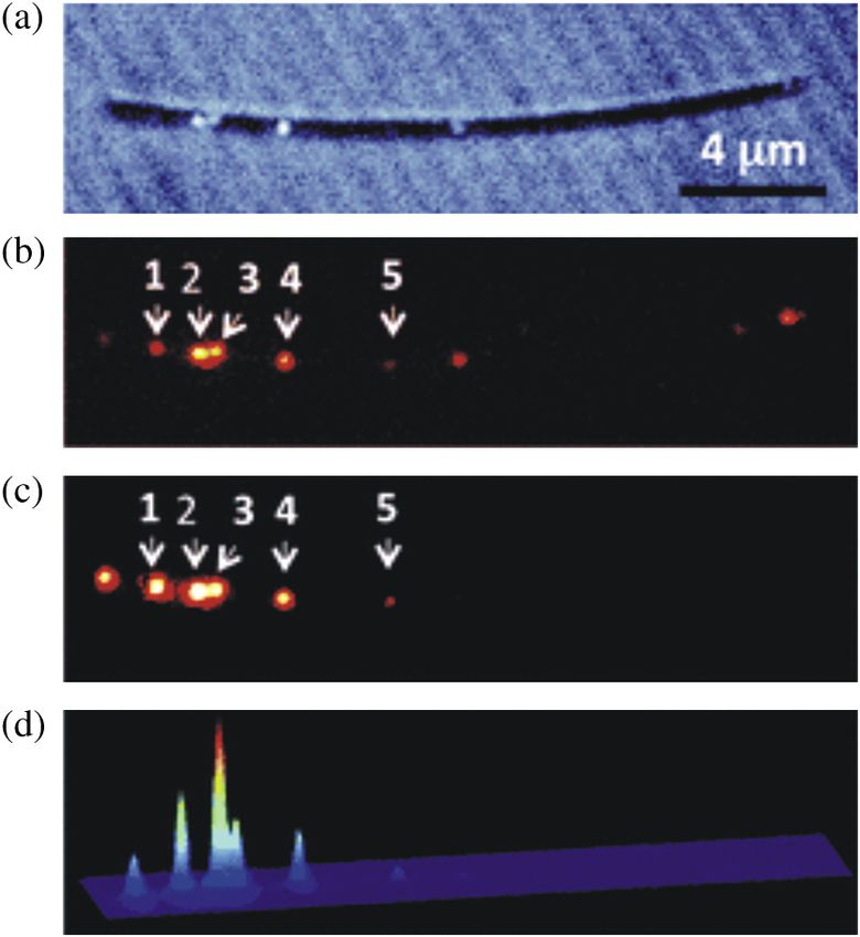
Kumar: Plasmonic nano-architectures for surface enhanced Raman scattering: a review

                                     Another important category of nanoparticles are the core-shell nanostructures,64 or the nano-
                                 shells.65–67 One of the major advantages of the shell-based nanoparticle is the ability to tune the
                                 plasmon resonance by tuning the physical and chemical parameters of both the shell and the core
                                 substance.13,68,69 Such nanoshell geometries have now found applications as tunable SERS sub-
                                 strates.13 An added advantage of this configuration is that two different kinds of nanomaterials
                                 can be incorporated as core and shell. For example, one can synthesize a nanoparticle with mag-
                                 netic core and a plasmonic shell,70 thereby making the nanoparticle not only sensitive to light but
                                 also an external magnetic field. Such magnetic core metallic nanostructures can be utilized as
                                 probes for magnetic resonance imaging (MRI), which is an important diagnostic tool. Due to
                                 their versatile optical properties, nanoshells also have good potential as probes for photothermal
                                 treatment of cancer, as revealed recently.68

                                 3.2 Nanocubes
                                 Precisely shaped plasmonic nanocubes have been recently synthesized71–78 and studied in the
                                 context of SERS. One of the advantages of nanocubes is their equidistant sharp edges that facil-
                                 itate highly localized optical fields, which can be harnessed to enhance Raman scattering sig-
                                 natures. In order to test the effect of edge sharpness, Xia and co-workers prepared isolated Ag
                                 nanocubes with sharp and truncated edges71 as shown in SEM images of Fig. 2. A thin layer of
                                 1,4-benzenedithiol (1,4 BDT) was adsorbed on these nanocubes and a linearly polarized Raman
                                 excitation laser of 514 nm was incident on these individual nanocubes and the polarization was
                                 varied as shown in the Fig. 2. The Raman spectra in Fig. 2(a)–2(c) represent the polarization
                                 dependent SERS signatures from sharply-edged Ag nanocubes corresponding to the directions
                                 indicated on the SEM images. The data indicated that when the polarization is aligned along one
                                 of the edges of the nanocube, the Raman signal intensity is enhanced. In contrast, Fig. 2(d)–2(f)
                                 shows that when the edges are truncated, the SERS signature is independent of the polarization
                                 of Raman excitation. This observation was also supported by polarization dependent discrete
                                 dipole approximation calculation of near-fields, which indicated that field enhancement
                                 along the diagonal of the sharp-edged nanocubes was greater for the aligned electric field.

                                 Fig. 2 Normalized SERS spectra of 1,4-BDT adsorbed on a Ag nanocube with sharp corners [left
                                 panel, (a)–(c)] and a highly truncated Ag nanocube [right panel, (d–(f)], at various angles relative
                                 to.the polarization of the excitation laser. Each SEM image shows the nanocube used and the
                                 arrows indicate the polarization directions of the incident laser corresponding to the spectra.
                                 The scale bar applies to both images. Reproduced with permission from Ref.

                                 Journal of Nanophotonics                              064503-4                            Vol. 6, 2012

Downloaded From: https://www.spiedigitallibrary.org/journals/Journal-of-Nanophotonics on 18 Nov 2020
Terms of Use: https://www.spiedigitallibrary.org/terms-of-use
Kumar: Plasmonic nano-architectures for surface enhanced Raman scattering: a review
Camargo et al.74 have further extrapolated this work to show that SERS hot-spots can be isolated
and probed by bringing two silver nanocubes close to each other. By employing a technique
based on plasma etching of molecules, they isolated the molecules from all parts of the nanocube
dimer except for the gap between them, thereby exclusively measuring the SERS signal between
the coupled nanocubes. Such innovation can be further harnessed and applied to other plasmonic
dimer nanostructures, where the SERS contribution from the gap junction is to be probed exclu-
sively. Recently, Rycenga et al.,78 have also shown that single silver nanocubes placed on metal-
lic substrates can facilitate single molecule SERS sensitivity. Their strategy was to use coupling
between the sharp edges of the nanocube with metallic layer underneath it. This coupling effec-
tively provides a reproducible hot-spot with large field enhancement, thereby leading to ultra-
sensitive SERS effect on a consistent basis. Plasmon coupling effects have also been observed75
in two-dimensionally (2-D) ordered gold nanocubes on indium tin oxide substrates indicating
that nanocube geometries are good substrates to study certain fundamental aspects of plasmonics
and SERS.
3.3 Nanotriangle
Another important category of plasmonic nanostructure that has been studied in the context
of SERS is nano-triangular patterns.79–81 Nanotriangles have sharp edges at their vertex
which facilitate localized optical fields, and hence can be harnessed for SERS applications.
One of the effective ways to produce patterns of nanotriangle pioneered by Van Dyune and
co-workers82,83,84 is to employ nanosphere lithography (NSL), which is an inexpensive, versatile,
and inherently parallel lithography method. Briefly, the procedure of NSL is as follows. First,
size-monodisperse nanospheres are self assembled on a substrate such as glass to form a 2-D
colloidal crystal deposition mask [see Fig. 3(a)]. Second, upon solvent evaporation, the desired
metal is deposited either by thermal evaporation or electron beam deposition, or pulsed laser
deposition through the nanosphere mask. Next, the nanosphere mask is removed by sonication
of the sample in a solvent, thereby leaving behind the metal deposited in the interstitials of the
nanosphere mask. A typical sample prepared using NSL is shown in Fig. 3(b). One of the major
advantages of this technique is that it can be modified to vary the size, shape and arrangement of
Fig. 3 Schematic illustration of a colloidal crystal mask (a) and representative AFM image (b) of
Ag nanotriangular stuructures. Reproduced with permission from Ref. 82. (c) SERS enhancement
achieved from R6G adsorbed on ordered 200 nm Ag nanocluster regions (gray trace) in compar-
ison with amorphous Ag “film” regions (black trace) within the same sample. The signal increase is
∼3×. Reproduced with permission from Ref. 90.
Journal of Nanophotonics 064503-5 Vol. 6, 2012
Downloaded From: https://www.spiedigitallibrary.org/journals/Journal-of-Nanophotonics on 18 Nov 2020
Terms of Use: https://www.spiedigitallibrary.org/terms-of-useKumar: Plasmonic nano-architectures for surface enhanced Raman scattering: a review
the plasmonic nanostructures.85–89 Schmidt et al.90 employed NSL to study SERS properties of
triangular shaped silver nanocluster arrays. They made direct comparison of rhodamine 6G
SERS signals between ordered nanocluster region and amorphous Ag regions in the same sample
[Fig. 3(c)]. The authors found that for the case of nanotriangles, the SERS signal intensity was
enhanced by a factor of 3 compared to amorphous Ag regions, indicating large electromagnetic
fields facilitated by the edges of the nanotriangles.
Another category similar to triangular geometry is the plasmonic nanopyramids.91–94 Stoer-
zinger et al.91 have recently screened individual gold nanopyramid shells and their assembly in a
systematic way. The authors employed fabrication methods involving phase-shifting photolitho-
graphy, etching, E-beam, and lift off (PEEL) procedures to create plasmonic nanopyramids, and
by controlling the evaporation rates of the solvent of nanopyriamids, they could assemble them
in three different categories: isolated single pyramids, lower order assembly, and higher order
assembly (Fig. 4). They observed that as the order of assembly increased, the Raman signal
intensity increased. They supported their experimental data with numerical simulations that
indicated enhanced electromagnetic field between adjacent particle faces in the higher order
structure. Such hierarchical nanostructures are useful to produce few-particle localized electro-
magnetic fields in a controlled fashion.
Fig. 4 (a) (top) SEM and (bottom) corresponding Raman images of the 1624 cm−1 MB vibrational
mode intensity from a single tip-down pyramid (TD), a low-order dimer of pyramidal nanoshells
(L2), and a high-order dimer of pyramidal nanoshells (H2). The scale bar applies to all images. (b)
Dark-field scattering spectra of TD, L2, and H2. (c) Raman spectra corresponding to the most
intense point of the Raman image in (a). Reproduced with permission from Ref. 91.
Journal of Nanophotonics 064503-6 Vol. 6, 2012
Downloaded From: https://www.spiedigitallibrary.org/journals/Journal-of-Nanophotonics on 18 Nov 2020
Terms of Use: https://www.spiedigitallibrary.org/terms-of-useKumar: Plasmonic nano-architectures for surface enhanced Raman scattering: a review
3.4 Nano-Rods
Nanorods are one of the extensively studied anisotropic plasmonic geometries.69,95–99 Various
research groups have studied optical properties of gold nanorods69,98–102 and have utilized them
for a variety of applications.97 Owing to their anisotropic geometry, nanorods exhibit two plas-
mon modes: transverse and longitudinal.96 The transverse plasmon mode is at lower wavelength
and the longitudinal mode is at higher wavelength. The longitudinal plasmon mode is sensitive to
the aspect ratio of the nanorod, and hence can be utilized in wavelength dependent studies. One
of the important issues in plasmonics is to understand how plasmons in individual nanostructures
can be coupled to obtain enhanced electromagnetic interactions. In this context, gold nanorods
have been employed to study the plasmon coupling in anisotropic nanostructures.69,98,101,103,104
Kumar and Thomas104 recently investigated the SERS properties of individual nanorods and
their assembly. The authors chemically couple the 111 plane at the edges of Au nanorods
with linker molecules and show that the SERS signature is enhanced when the rods are in
dimer geometry (Fig. 5). They further show that end-to-end coupling can be extended to
form a linear chain of Au nanorods leading to an enhanced signature in Raman intensity.
Such linear chains of anisotropic nanorods are good candidates to study sub-diffraction plas-
monic coupling and electromagnetic transport.
Since Au nanorods are anisotropic in their geometry, they are sensitive to linear polarization
of incident radiation. El-Sayed and co-workers105 have utilized this polarization dependence to
show that Au nanorods conjugated with antibodies can be aligned and assembled on the surface
of cancer cells. They further show that such aligned assembly of nanorods can be used as cancer
diagnostic markers. Such innovations have opened up avenues for biological applications of
nanorod based SERS.
3.5 Nano-Wires
Plasmonic nanowires are unique substrates as they support propagating plasmon polari-
tons.12,106–111 They sustain plasmon modes with wavelengths shorter than the incident light.
Interestingly, chemically synthesized plasmonic nanowires,112,113 such as Ag nanowires,
show minimal plasmon damping due to well-defined crystal structure, and hence have been
employed in studies of plasmon polariton based waveguiding.111,114–118 In the context of
SERS, coupling of an individual nanowire to another plasmonic nanostructure119–121 creates
a spatially confined SERS hot spot at the junctions. One of the recent innovations in nano-
wire-based SERS is the remote excitation of Raman scattering.120,122 The authors have
shown that the propagating plasmon property of the plasmonic nanowires can be used to perform
Raman scattering at a remote location (see Fig. 6). By exciting the plasmon polariton at one end
of the nanowire, a source of light can be created at the distal end of the nanowire, which further
can be utilized as a Raman excitation source. The advantage of this technique is that the Raman
Fig. 5 TEM images of gold nanorods (a)–(c) in isolated, dimer, and chain configurations; and
Raman spectrum of molecule bipy-DT (d)–(f) at various stages of plasmon coupling. Reproduced
with permission from Ref. 104.
Journal of Nanophotonics 064503-7 Vol. 6, 2012
Downloaded From: https://www.spiedigitallibrary.org/journals/Journal-of-Nanophotonics on 18 Nov 2020
Terms of Use: https://www.spiedigitallibrary.org/terms-of-useKumar: Plasmonic nano-architectures for surface enhanced Raman scattering: a review
Fig. 6 Transmission (a), wide-field illumination (b), and focused laser excitation (c) images of a
NPs-pATP-nanowire exhibiting seven SERS hot-spots. Focused excitation was at the left end of
the wire in panel (c). (d) 3-D view of the image in panel (c). Reproduced with permission from
Ref. 122.
excitation source is confined to the apex of the nanowire, and is devoid of background radiation
of incident laser excitation (Fig. 6). Thus by separating the channels of excitation source and
Raman scattering source, molecules in the vicinity of the distal end of the nanowire can be
probed at high spatial resolution. Nanowires have also been utilized to create SERS hot-
spots.122–124 Recently, Chikkaraddy et al.124 have shown that by coupling two plasmonic nano-
wires in an end-to-end configuration, SERS hot-spots can be created at the nanowire junction.
The advantage of this method is that the end-to-end coupling configuration not only facilitates
SERS hot-spot, but also provides SPP based light propagation capability from one end of the
nanowire pair to other distal end.
3.6 Nanotips
Although SERS microscopy facilitates large scale enhancement factors, it is constrained by the
diffraction limit, and hence cannot spatially resolve entities smaller than the Raman excitation
wavelength. Tip enhanced Raman scattering (TERS)125–129 has recently emerged as method to
perform vibrational spectroscopy beyond diffraction limit. The technique employed in TERS is
essentially borrowed from apertureless near-field optical microscopy, where a sharp metallic tip
is brought into close proximity of the sample deposited on the surface 130–132 The tip facilitates
the localized optical field which interacts with molecules beneath it, thus enhancing the Raman
signal intensity. One of the important components in TERS is the morphology and composition
of the tip.125,133–140 The radius of curvature of the apex of the tip determines the spatial resolu-
tion,134 and hence it is necessary to fabricate high quality plasmonic nano-tip. The most popular
configuration of the tip used in TERS is a gold or silver nano-tip.134 This is usually prepared by
chemical etching of wire.138 Another method to peform TERS is to employ a plasmonic nano-
particle attached to dielectric tip.141,142
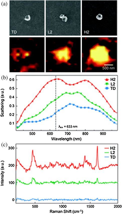
In recent times, an alternative method based on adiabatic focusing of plasmons at the apex of
the tip has been introduced to perform TERS by Raschke and co-workers.143 The advantage of
this method is the non-local generation of nanoscale Raman excitation source which facilitates
intrinsic background suppression of Raman pump beam. This was achieved by cutting a grating
on a chemically etched plasmon nano-tip (Fig. 7) and exciting it with Raman pump beam.
Propagating plasmons are generated due to this coupling, and further propagate towards the
apex of the tip, thus creating a nanoscale light source at the discontinuity. This light source
Journal of Nanophotonics 064503-8 Vol. 6, 2012
Downloaded From: https://www.spiedigitallibrary.org/journals/Journal-of-Nanophotonics on 18 Nov 2020
Terms of Use: https://www.spiedigitallibrary.org/terms-of-useKumar: Plasmonic nano-architectures for surface enhanced Raman scattering: a review
Fig. 7 (a) Schematic of the adiabatic nanofocus based the Raman scattering experiment.
Electrochemically etched Au tips are mounted onto the quartz tuning fork of a shear-force
AFM, and a grating is cut using FIB. Incident light is focused onto the grating, and the Raman
scattered light excited by the nanofocused SPP at the apex is detected at a 90-deg angle. (b)
SEM micrograph of an electrochemically etched Au tip superimposed with optical image of grating
illumination and apex emission. (c) Grating-coupled TERS distance dependence for λ ¼ 632.8 nm
of Malachite Green on a Au surface. Reproduced with permission from Ref. 143.
can be harnessed to perform Raman spectroscopy as shown in Fig. 7(c). Adiabatic nano-focusing
is an efficient method of converting far-field optical signal into near-field localized light
source,144 and has immense potential to perform background-free nanoscale chemical spectros-
copy and imaging.145–149
Recently, Capasso and co-workers150 have also shown that optical antenna arrays can be
fabricated on an optical fiber and can be utilized as SERS micro-probes, thus expanding the
prospects of in situ SERS detection.
4 Unconventional Nano-Architectures for SERS
Until now we have discussed plasmonic substrates that are conventionally used for SERS appli-
cations. In recent times, there have been innovations on plasmonic nanostructures designed
either to probe specific issues in SERS or integrate SERS with other experimental modules.
Below we briefly discuss a few cases:
• Electrostatic force based SERS—Lacharmoise et al.151 have come up with an electro-
chemistry based approach to guide charged molecules in a solution towards SERS active
nanostructures. The authors show the possibility to selectively enhance SERS signal of
various types of dye molecules according to their charge. They prepared an electrolytic
cell in which charged species were selectively attracted towards SERS substrate by apply-
ing a direct current (DC) electric field. Such attracted species give rise to enhanced Raman
signatures. The authors envisage their method to be useful in single molecule SERS situa-
tions where precise placement of molecules in hot-spot is a necessity.
• Shell-Isolated Nanoparticle based SERS—Although SERS is a powerful analytical tech-
nique with single molecule sensitivity, it critically depends on interaction of molecules
with metallic nanostructures. Gaining control over this interaction is one of the challenges
in SERS, and one of the methods towards this goal is the shell-isolated nanoparticle
approach innovated by Tian and co-workers.152,153 In this method, the Raman signal is
Journal of Nanophotonics 064503-9 Vol. 6, 2012
Downloaded From: https://www.spiedigitallibrary.org/journals/Journal-of-Nanophotonics on 18 Nov 2020
Terms of Use: https://www.spiedigitallibrary.org/terms-of-useKumar: Plasmonic nano-architectures for surface enhanced Raman scattering: a review
enhanced by gold nanoparticles with an ultrathin silica or alumina shell. In order to probe
the surface of interest, a thin layer of such core-shell nanoparticle is spread as ‘smart dust’.
The advantages of this method are: 1. the aggregation of nanoparticles is avoided due to
thin protective shell, and 2. the metallic probe is not in direct contact with the probed
material. The proof of concept of this SERS technique has been shown to enhance
signatures of molecules on yeast cells and citrus fruits with pesticide residues.152
• Double resonance based SERS—There are three important spectral regions in Raman
spectroscopy: first is the Raman excitation region, second is the Stokes intensity region,
and third is the anti-Stokes intensity region. In order to enhance the Raman intensity
signatures via SERS, it would be beneficial to have plasmon resonances that overlap
with these regions. By tuning the geometrical arrangement of plasmonic nanostructures,
Cohen and co-workers154–157 have developed double-resonance SERS substrates. One of
the methods154 to prepare double resonance substrate is to deposit gold nanodisk on SiO2
coated gold film. The gold nanodisk facilitates localized surface plasmon, and the dielec-
tric-metal interface facilitates surface plasmon polaritons. By varying the experimental
parameters, such as the geometrical arrangement of gold nanodisk and the angle of incident
light, one could fabricate plasmonic substrates with double resonances. Another method155
is to use a pair of different shaped plasmonic nanostructures which inherently show
plasmon resonances at different locations of the spectra. Such double resonance SERS
substrates have shown to have better enhancement capabilities154,155 compared to single
resonance substrates.
• SERS in optofluidic chip—Performing Raman scattering in lab-on-chip configuration
has various advantages such as minimal sample requirement, compactness, and cost-
effectiveness. Integration of SERS with optofluidic configurations is an active area of
research.158–166 Most of the techniques either use nanoparticle-based microfluidic
systems167–171 or embedded plasmonic substrates172,173 in fluidic channels to attain high
sensitivity and chemical specificity. The envisaged application includes environmental
monitoring, clinical diagnostics, forensic investigations, and homeland security.
5 Future Directions and Conclusion
SERS is now a matured research field that requires a multidisciplinary approach and fosters the
combination of ideas from physics, chemistry, biology, and engineering. Although SERS is now
routinely used as analytical tool for characterization of plasmonic substrates, there are some
issues that require greater attention, such as:
1. Design and execution of a plasmonic substrates with consistent Raman enhancement
factors.
2. Better understanding of the physics behind the SERS hot-spot mechanism.
3. Understanding the mechanism behind the chemical enhancement factor and how it can be
harnessed for applications.
4. Plasmon-assisted vibrational pumping mechanism and how it can be used to get deeper
insight into molecular structure and function.
Recently, there are a few developments in other research areas where SERS may play an
important role. Following are a few examples:
1. There is an active search for new and better plasmonic materials.174 It has been postu-
lated174,175 that nanomaterials made of metal oxides, noble-transition alloys, alkali-noble
inter-metallic compounds, semiconductors, and graphene can exhibit plasmonic proper-
ties. Sol-gel based photonic structures176 have also been explored and shown to exhibit
light management capabilities that can be adapted to perform SERS. Such materials will
expand the avenues for SERS substrates and can be utilized for specific applications.
2. There has been tremendous progress made in the field of ultra-fast optics which has
led to laser sources that can provide very high temporal resolutions (femto-seconds to
atto-seconds). Concomitantly, there has been great progress made in scanning probe
techniques that can provide spatial resolution up to a single atom. Combining both
Journal of Nanophotonics 064503-10 Vol. 6, 2012
Downloaded From: https://www.spiedigitallibrary.org/journals/Journal-of-Nanophotonics on 18 Nov 2020
Terms of Use: https://www.spiedigitallibrary.org/terms-of-useKumar: Plasmonic nano-architectures for surface enhanced Raman scattering: a review
techniques177,178 can greatly influence the spatial and temporal resolution of chemical
imaging methods, such as SERS. Non-linear Raman scattering techniques, such as coher-
ent anti-Stokes Raman scattering (CARS) and stimulated Raman scattering can also be
combined with the concepts of plasmonics. Recently, there have been a few reports177,179–
183
that show plenty of promise in this direction.
3. Gaining new insight into the light-matter interaction has been one of the important issues
in physics, and the question is how SERS can contribute to this. In recent times, SERS has
been able contribute towards the understanding of ultrafast non-radiative decay rates of
single molecules on metallic surfaces.184 Galloway et al. have quantified the total decay
rate of single emitters close to the metallic surface, which is difficult to estimate using
conventional approaches.184 In a different study, Rao et al.,185 have experimentally mea-
sured mechanical forces induced by SERS on an optically trapped dielectric sphere. The
authors revealed a correlation between the enhancement of the Raman signal and the
average position of the trapped bead indicating momentum transfer of the emitted
Raman photons on to the trapped bead.
4. Single molecule junction is one of the important components of molecular electronics that
is being studied. A few research groups186,187 have employed SERS as an effective method
to probe the structure of molecular junctions. Recent developments by Liu et al.,187
includes a technique called as ‘fishing-mode’ tip enhanced Raman spectroscopy that
can measure electrical conductance and Raman spectroscopy signals of a single molecule
in a junction. Ward et al.,186 have used SERS to determine the effective temperature of a
biased metallic nano-junction decorated with molecules, which leads to the better under-
standing of nanoscale heating mechanisms.
Thus, we see how interaction of molecules with plasmonic nanomaterials has opened up new
research avenues. Techniques such as SERS contribute to our understanding of both the plas-
monic nanomaterial and the molecule interacting with it, thus making them an extremely useful
tool in nano-optics and spectroscopy. In the context of nano-science and -technology, Richard
Feynman had prophetically predicted that, ‘There’s plenty of room at the bottom’.188 Plasmonic
nanomaterials combined with nano-optical techniques have shown how insightful his predic-
tion was.
Acknowledgments
The author thanks Department of Science and Technology (DST), India for Ramanujan fellow-
ship. This research was partially funded by DST NANOSCIENCE UNIT GRANT (SR/NM/NS-
42/2009) at IISER-P.
References
1. A. Biswas et al., “Advances in top-down and bottom-up surface nanofabrication: techni-
ques, applications & future prospects,” Advances in Colloid and Interface Science in press,
DOI: 10.1016/j.bbr.2011.03.031 (2012).
2. C. Vieu et al., “Electron beam lithography: resolution limits and applications,” Appl. Surf.
Sci. 164, 111–117 (2000), http://dx.doi.org/10.1016/S0169-4332(00)00352-4.
3. G. M. Whitesides and B. Grzybowski, “Self-assembly at all scales,” Science 295,
2418–2421 (2002), http://dx.doi.org/10.1126/science.1070821.
4. B. D. Gates et al., “Unconventional nanofabrication,” Annu. Rev. Mater. Res. 34, 339–372
(2004), http://dx.doi.org/10.1146/annurev.matsci.34.052803.091100.
5. P. Maury et al., in Materials Research Society Symposium Proceedings, Vol. 901, pp.
441–449, Cambridge University Press, Cambridge, UK (2005).
6. U. Kreibig and M. Vollmer, Optical Properties of Metal Clusters, Springer, Berlin (1995).
7. H. Raether, Surface Plasmons on Smooth and Rough Surfaces and on Gratings, Springer,
Berlin (1988).
8. S. A. Kalele et al., “Plasmon-assisted photonics at the nanoscale,” J. Nanophoton. 1, 12501
(2007), http://dx.doi.org/10.1117/1.2748429.
Journal of Nanophotonics 064503-11 Vol. 6, 2012
Downloaded From: https://www.spiedigitallibrary.org/journals/Journal-of-Nanophotonics on 18 Nov 2020
Terms of Use: https://www.spiedigitallibrary.org/terms-of-useKumar: Plasmonic nano-architectures for surface enhanced Raman scattering: a review
9. W. L. Barnes, A. Dereux, and T. W. Ebbesen, “Surface plasmon subwavelength optics,”
Nature 424, 824–830 (2003), http://dx.doi.org/10.1038/nature01937.
10. V. M. Shalaev, “Electromagnetic properties of small-particle composites,” Phys. Rep. 272,
61–137 (1996), http://dx.doi.org/10.1016/0370-1573(95)00076-3.
11. A. V. Zayats, II Smolyaninov, and A. A. Maradudin, “Nano-optics of surface plasmon
polaritons,” Phys. Rep.-Rev. Sect. Phys. Lett. 408, 131–314 (2005).
12. Surface plasmon nanophotonics; Springer Series in Optical Sciences, Vol. 131, P. G.Kik
and M. L. Brongersma, ed. Springer, Dordrecht (2007).
13. S. Lal, S. Link, and N. J. Halas, “Nano-optics from sensing to waveguiding,” Nat. Photon.
1, 641–648 (2007), http://dx.doi.org/10.1038/nphoton.2007.223.
14. T. H. Taminiau et al., “Optical antennas direct single-molecule emission,” Nat. Photon. 2,
234–237 (2008), http://dx.doi.org/10.1038/nphoton.2008.32.
15. M. Moskovits, “Surface-enhanced spectroscopy,” Rev. Mod. Phys. 57, 783–826 (1985),
http://dx.doi.org/10.1103/RevModPhys.57.783.
16. C. D. Geddes and J. R. Lakowicz, “Metal-Enhanced Fluorescence,” J. Fluores. 12,
121–129 (2002), http://dx.doi.org/10.1023/A:1016875709579.
17. G. L. Liu et al., “Quantized plasmon quenching dips nanospectroscopy via plasmon reso-
nance energy transfer,” Nat. Methods 4, 1015–1017 (2007), http://dx.doi.org/10.1038/
nmeth1133.
18. P. L. Stiles et al., “Surface-enhanced Raman spectroscopy,” Annu. Rev. Anal. Chem. 1,
601–626 (2008), http://dx.doi.org/10.1146/annurev.anchem.1.031207.112814.
19. R. F. Aroca, Surface-Enhanced Vibrational Spectroscopy, Wiley, West Sussex (2006).
20. E. C. Le Ru and P. G. Etchegoin, Principles of Surface-Enhanced Raman Spectroscopy
and Related Plasmonic Effects, Elsevier, Amsterdam (2009).
21. M. Fleischmann, P. J. Hendra, and A. J. McQuillan, “Raman spectra of pyridine adsorbed
at a silver electrode,” Chem. Phys. Lett. 26, 163–166 (1974), http://dx.doi.org/10.1016/
0009-2614(74)85388-1.
22. D. L. Jeanmaire and R. P. Van Duyne, “Surface Raman spectroelectrochemistry part I.
heterocyclic, aromatic, and aliphatic amines adsorbed on the anodized silver electrode,”
J. Electroanal. Chem. 84, 1–20 (1977), http://dx.doi.org/10.1016/S0022-0728(77)80224-6.
23. M. G. Albrecht and J. A. Creighton, “Anomalously intense Raman spectra of pyridine at a
silver electrode,” J. Am. Chem. Soc. 99, 5215–5217 (1977), http://dx.doi.org/10.1021/
ja00457a071.
24. G. C. Schatz, “Theoretical studies of surface enhanced Raman scattering,” Accounts.
Chem. Res. 17, 370–376 (1984), http://dx.doi.org/10.1021/ar00106a005.
25. M. Moskovits, “Surface-enhanced Raman spectroscopy: a brief retrospective,” J. Raman
Spectros. 36, 485–496 (2005), http://dx.doi.org/10.1002/(ISSN)1097-4555.
26. A. Otto et al., “Surface-enhanced Raman scattering,” J. Phys.: Condens. Matt. 4,
1143–1212 (1992), http://dx.doi.org/10.1088/0953-8984/4/5/001.
27. A. Campion et al., “On the mechanism of chemical enhancement in surface-enhanced
Raman scattering,” J. Am. Chem. Soc. 117, 11807–11808 (1995), http://dx.doi.org/10
.1021/ja00152a024.
28. A. Campion and P. Kambhampati, “Surface-enhanced Raman scattering,” Chem. Soc. Rev.
27, 241–250 (1998), http://dx.doi.org/10.1039/a827241z.
29. E. C. Le Ru et al., “Surface enhanced Raman scattering enhancement factors: a compre-
hensive study,” J. Phys. Chem. C 111, 13794–13803 (2007), http://dx.doi.org/10.1021/
jp0687908.
30. E. C. Le Ru and P. G. Etchegoin, “Rigorous justification of the jEj4^ enhancement factor in
surface enhanced Raman spectroscopy,” Chem. Phys. Lett. 423, 63–66 (2006), http://dx
.doi.org/10.1016/j.cplett.2006.03.042.
31. J. Zhao et al., “Methods for describing the electromagnetic properties of silver and gold
nanoparticles,” Accounts Chem. Res. 41, 1710–1720 (2008), http://dx.doi.org/10.1021/
ar800028j.
32. L. Brus, “Noble metal nanocrystals: plasmon electron transfer photochemistry and single-
molecule Raman spectroscopy,” Accounts Chem. Res. 41, 1742–1749 (2008), http://dx.doi
.org/10.1021/ar800121r.
Journal of Nanophotonics 064503-12 Vol. 6, 2012
Downloaded From: https://www.spiedigitallibrary.org/journals/Journal-of-Nanophotonics on 18 Nov 2020
Terms of Use: https://www.spiedigitallibrary.org/terms-of-useKumar: Plasmonic nano-architectures for surface enhanced Raman scattering: a review
33. J. P. Camden et al., “Controlled plasmonic nanostructures for surface-enhanced spectroscopy
and sensing,” Accounts Chem. Res. 41, 1653–1661 (2008), http://dx.doi.org/10.1021/
ar800041s.
34. T. Dadosh et al., “Plasmonic control of the shape of the Raman spectrum of a single mole-
cule in a silver nanoparticle dimer,” ACS Nano 3, 1988–1994 (2009), http://dx.doi.org/10
.1021/nn900422w.
35. J. Jiang et al., “Single molecule Raman spectroscopy at the junctions of large Ag nano-
crystals,” J. Phys. Chem. B 107, 9964–9972 (2003), http://dx.doi.org/10.1021/jp034632u.
36. J. R. Lombardi, R. L. Birke, and G. Haran, “Single molecule SERS spectral blinking and vibro-
nic coupling,” J. Phys.Chem. C 115, 4540–4545 (2011), http://dx.doi.org/10.1021/jp111345u.
37. J. P. Camden et al., “Probing the structure of single-molecule surface-enhanced Raman
scattering hot spots,” J. Am. Chem. Soc. 130, 12616–12617 (2008), http://dx.doi.org/
10.1021/ja8051427.
38. J. A. Dieringer et al., “A frequency domain existence proof of single-molecule surface-
enhanced Raman spectroscopy,” J. Am. Chem. Soc. 129, 16249–16256 (2007), http://dx
.doi.org/10.1021/ja077243c.
39. E. C. Le Ru et al., “A scheme for detecting every single target molecule with surface-
enhanced raman spectroscopy,” Nano Lett. 11, 5013–5019 (2011), http://dx.doi.org/10
.1021/nl2030344.
40. K. Kneipp et al., “Single molecule detection using surface-enhanced Raman scattering
(SERS),” Phys. Rev. Lett. 78, 1667–1670 (1997), http://dx.doi.org/10.1103/
PhysRevLett.78.1667.
41. S. Nie and S. R. Emory, “Probing single molecules and single nanoparticles by surface-
enhanced Raman scattering,” Science 275, 1102–1106 (1997), http://dx.doi.org/10.1126/
science.275.5303.1102.
42. P. C. Lee and D. Meisel, “Adsorption and surface-enhanced Raman of dyes on silver and
gold sols,” J. Phys. Chem. 86, 3391–3395 (1982), http://dx.doi.org/10.1021/j100214a025.
43. J. A. Creighton, C. G. Blatchford, and M. G. Albrecht, “Plasma resonance enhancement of
Raman scattering by pyridine adsorbed on silver or gold sol particles of size comparable to
the excitation wavelength,” Journal of the Chemical Society, Faraday Transactions 2:
Molecular and Chemical Physics 75, 790–798 (1979).
44. M. Kerker, “The optics of colloidal silver: something old and something new,” J. Colloid
Interface Sci. 105, 297–314 (1985), http://dx.doi.org/10.1016/0021-9797(85)90304-2.
45. K. Kneipp et al., “Surface-enhanced Raman scattering and biophysics,” J. Phys. Condens.
Matter. 14, R597–R624 (2002), http://dx.doi.org/10.1088/0953-8984/14/18/202.
46. W. Li et al., “Dimers of silver nanospheres: Facile synthesis and their use as hot spots for
surface-enhanced Raman scattering,” Nano Lett. 9, 485–490 (2009), http://dx.doi.org/10
.1021/nl803621x.
47. F. Svedberg et al., “Creating hot nanoparticle pairs for surface-enhanced Raman spectro-
scopy through optical manipulation,” Nano Lett. 6, 2639–2641 (2006), http://dx.doi.org/10
.1021/nl062101m.
48. C. E. Talley et al., “Surface-enhanced Raman scattering from individual Au nanoparticles
and nanoparticle dimer substrates,” Nano Lett. 5, 1569–1574 (2005), http://dx.doi.org/10
.1021/nl050928v.
49. H. Wang, C. S. Levin, and N. J. Halas, “Nanosphere arrays with controlled sub-10-nm
gaps as surface-enhanced Raman spectroscopy substrates,” J. Am. Chem. Soc. 127,
14992–14993 (2005), http://dx.doi.org/10.1021/ja055633y.
50. M. Rycenga et al., “Understanding the SERS effects of single silver nanoparticles and their
dimers, one at a time,” J. Phys. Chem. Lett. 1, 696–703 (2010), http://dx.doi.org/10.1021/
jz900286a.
51. K. L. Wustholz et al., “Structure-activity relationships in gold nanoparticle dimers
and trimers for surface-enhanced Raman spectroscopy,” J. Am. Chem. Soc. 132,
10903–10910 (2010), http://dx.doi.org/10.1021/ja104174m.
52. S. M. Stranahan, E. J. Titus, and K. A. Willets, “SERS orientational imaging of silver
nanoparticle dimers,” J. Phys. Chem. Lett. 2, 2711–2715 (2011), http://dx.doi.org/10
.1021/jz201133p.
Journal of Nanophotonics 064503-13 Vol. 6, 2012
Downloaded From: https://www.spiedigitallibrary.org/journals/Journal-of-Nanophotonics on 18 Nov 2020
Terms of Use: https://www.spiedigitallibrary.org/terms-of-useKumar: Plasmonic nano-architectures for surface enhanced Raman scattering: a review
53. S. Bidault, F. J. GarcÃa De Abajo, and A. Polman, “Plasmon-based nanolenses assembled
on a well-defined DNA template,” J. Am. Chem. Soc. 130, 2750–2751 (2008), http://dx.doi
.org/10.1021/ja711074n.
54. W. Rechberger et al., “Optical properties of two interacting gold nanoparticles,” Opt. Com-
mun. 220, 137–141 (2003), http://dx.doi.org/10.1016/S0030-4018(03)01357-9.
55. T. Atay, J. H. Song, and A. V. Nurmikko, “Strongly interacting plasmon nanoparticle pairs:
from dipole-dipole interaction to conductively coupled regime,” Nano Lett. 4, 1627–1631
(2004), http://dx.doi.org/10.1021/nl049215n.
56. J. N. Anker et al., “Biosensing with plasmonic nanosensors,” Nat. Materials 7, 442–453
(2008), http://dx.doi.org/10.1038/nmat2162.
57. J. B. Lassiter et al., “Close encounters between two nanoshells,” Nano Lett. 8, 1212–1218
(2008), http://dx.doi.org/10.1021/nl080271o.
58. N. J. Halas et al., “Plasmons in strongly coupled metallic nanostructures,” Chem. Rev. 111,
3913–3961 (2011), http://dx.doi.org/10.1021/cr200061k.
59. C. G. Khoury and T. Vo-Dinh, “Gold nanostars for surface-enhanced Raman scattering:
synthesis, characterization and optimization,” J. Phys. Chem. C 112, 18849–18859 (2008).
60. P. Senthil Kumar et al., “High-yield synthesis and optical response of gold nanostars,”
Nanotechnology 19, 015606 (2008), http://dx.doi.org/10.1088/0957-4484/19/01/015606.
61. E. Nalbant Esenturk and A. R. Hight Walker, “Surface-enhanced Raman scattering spec-
troscopy via gold nanostars,” J. Raman Spectros. 40, 86–91 (2009), http://dx.doi.org/10
.1002/jrs.v40:1.
62. S. Barbosa et al., “Tuning size and sensing properties in colloidal gold nanostars,” Lang-
muir 26, 14943–14950 (2010), http://dx.doi.org/10.1021/la102559e.
63. Q. Su et al., “A reproducible SERS substrate based on electrostatically assisted
APTES-functionalized surface-assembly of gold nanostars,” ACS Appl. Mater. Interfaces
3, 1873–1879 (2011), http://dx.doi.org/10.1021/am200057f.
64. R. Ghosh Chaudhuri and S. Paria, “Core/shell nanoparticles: classes, properties, synthesis
mechanisms, characterization, and applications,” Chemical Reviews in press, DOI:
10.1021/cr100449n (2012).
65. S. J. Oldenburg et al., “Nanoengineering of optical resonances,” Chem. Phys. Lett. 288,
243–247 (1998), http://dx.doi.org/10.1016/S0009-2614(98)00277-2.
66. R. D. Averitt, S. L. Westcott, and N. J. Halas, “Linear optical properties of gold nano-
shells,” J. Opt. Soc. Am. B 16, 1824–1832 (1999), http://dx.doi.org/10.1364/JOSAB.16
.001824.
67. J. B. Jackson and N. J. Halas, “Silver nanoshells: variations in morphologies and optical
properties,” J. Phys. Chem. B 105, 2743–2746 (2001), http://dx.doi.org/10.1021/
jp003868k.
68. S. Lal, S. E. Clare, and N. J. Halas, “Nanoshell-enabled photothermal cancer therapy:
impending clinical impact,” Accounts Chem. Res. 41, 1842–1851 (2008), http://dx.doi
.org/10.1021/ar800150g.
69. S. Lal et al., “Tailoring plasmonic substrates for surface enhanced spectroscopies,” Chem.
Soc. Rev. 37, 898–911 (2008), http://dx.doi.org/10.1039/b705969h.
70. L. R. Hirsch et al., “Nanoshell-mediated near-infrared thermal therapy of tumors under
magnetic resonance guidance,” Proceedings of the National Academy of Sciences of
the United States of America 100, 13549–13554 (2003), http://dx.doi.org/10.1073/pnas
.2232479100.
71. J. M. McLellan et al., “The SERS activity of a supported ag nanocube strongly depends on
its orientation relative to laser polarization,” Nano Lett. 7, 1013–1017 (2007), http://dx.doi
.org/10.1021/nl070157q.
72. L. J. Sherry et al., “Localized surface plasmon resonance spectroscopy of single silver
nanocubes,” Nano Lett. 5, 2034–2038 (2005), http://dx.doi.org/10.1021/nl0515753.
73. J. M. McLellan et al., “Comparison of the surface-enhanced Raman scattering on sharp
and truncated silver nanocubes,” Chem. Phys. Lett. 427, 122–126 (2006), http://dx.doi.org/
10.1016/j.cplett.2006.05.111.
74. P. H. C. Camargo et al., “Isolating and probing the hot spot formed between two silver
nanocubes,” Angewandte Chemie—International Edition 48, 2180–2184 (2009).
Journal of Nanophotonics 064503-14 Vol. 6, 2012
Downloaded From: https://www.spiedigitallibrary.org/journals/Journal-of-Nanophotonics on 18 Nov 2020
Terms of Use: https://www.spiedigitallibrary.org/terms-of-useKumar: Plasmonic nano-architectures for surface enhanced Raman scattering: a review
75. H. Chen et al., “Plasmon coupling in clusters composed of two-dimensionally ordered gold
nanocubes,” Small 5, 2111–2119 (2009), http://dx.doi.org/10.1002/smll.v5:18.
76. J. M. McMahon et al., “Correlating the structure, optical spectra, and electrodynamics of
single silver nanocubes,” J. Phys. Chem. C 113, 2731–2735 (2009), http://dx.doi.org/10
.1021/jp8098736.
77. E. Ringe et al., “Unraveling the effects of size, composition, and substrate on the localized
surface plasmon resonance frequencies of gold and silver nanocubes: a systematic single-
particle approach,” J. Phys. Chem. C 114, 12511–12516 (2010), http://dx.doi.org/10.1021/
jp104366r.
78. M. Rycenga et al., “Generation of hot spots with silver nanocubes for single-molecule
detection by surface-enhanced Raman scattering,” Angewandte Chemie—International
Edition 50, 5473–5477 (2011).
79. J. Zhao et al., “Localized surface plasmon resonance biosensors,” Nanomedicine 1,
219–228 (2006), http://dx.doi.org/10.2217/17435889.1.2.219.
80. W. A. Murray, J. R. Suckling, and W. L. Barnes, “Overlayers on silver nanotriangles: field
confinement and spectral position of localized surface plasmon resonances,” Nano Lett. 6,
1772–1777 (2006), http://dx.doi.org/10.1021/nl060812e.
81. K. A. Willets and R. P. Van Duyne, “Localized surface plasmon resonance spectroscopy
and sensing,” Annu. Rev. Phys. Chem. 267–297 (2007).
82. C. L. Haynes and R. P. Van Duyne, “Nanosphere lithography: A versatile nanofabrication
tool for studies of size-dependent nanoparticle optics,” J. Phys. Chem. B 105, 5599–5611
(2001), http://dx.doi.org/10.1021/jp010657m.
83. J. C. Hulteen et al., “Nanosphere lithography: size-tunable silver nanoparticle and surface
cluster arrays,” J. Phys. Chem. B 103, 3854–3863 (1999), http://dx.doi.org/10.1021/
jp9904771.
84. X. Zhang, C. R. Yonzon, and R. P. Van Duyne, “Nanosphere lithography fabricated plas-
monic materials and their applications,” J. Mater. Res. 21, 1083–1092 (2006), http://dx.doi
.org/10.1557/jmr.2006.0136.
85. G. L. Liu et al., “Magnetic nanocrescents as controllable surface-enhanced raman scatter-
ing nanoprobes for biomolecular imaging,” Adv. Materials 17, 2683–2688 (2005), http://
dx.doi.org/10.1002/(ISSN)1521-4095.
86. J. S. Shumaker-Parry, H. Rochholz, and M. Kreiter, “Fabrication of crescent-shaped opti-
cal antennas,” Adv. Materials 17, 2131–2134 (2005), http://dx.doi.org/10.1002/(ISSN)
1521-4095.
87. L. Yu et al., “Nanophotonic crescent moon structures with sharp edge for ultrasensitive
biomolecular detection by local electromagnetic field enhancement effect,” Nano Lett. 5,
119–124 (2005), http://dx.doi.org/10.1021/nl048232+.
88. R. Bukasov and J. S. Shumaker-Parry, “Highly tunable infrared extinction properties of
gold nanocrescents,” Nano Lett. 7, 1113–1118 (2007), http://dx.doi.org/10.1021/nl062317o.
89. A. Aubry et al., “Broadband plasmonic device concentrating the energy at the nanoscale:
the crescent-shaped cylinder,” Physical Review B—Condensed Matter and Materials
Physics 82, 125430 (2010).
90. J. P. Schmidt, S. E. Cross, and S. K. Buratto, “Surface-enhanced Raman scattering from
ordered Ag nanocluster arrays,” J. Chem. Phys. 121, 10657–10659 (2004), http://dx.doi
.org/10.1063/1.1799992.
91. K. A. Stoerzinger et al., “Screening nanopyramid assemblies to optimize surface enhanced
Raman scattering,” J. Phys. Chem. Lett. 1, 1046–1050 (2010), http://dx.doi.org/10.1021/
jz100095b.
92. B. Cui et al., “Fabrication of large area nanoprism arrays and their application for surface
enhanced Raman spectroscopy,” Nanotechnology 19, 145302 (2008), http://dx.doi.org/10
.1088/0957-4484/19/14/145302.
93. T. H. Lin et al., “Electrochemical SERS at periodic metallic nanopyramid arrays,” J. Phys.
Chem. C 113, 1367–1372 (2009), http://dx.doi.org/10.1021/jp809363m.
94. C. H. Sun, N. C. Linn, and P. Jiang, “Templated fabrication of periodic metallic nanopyr-
amid arrays,” Chem. Materials 19, 4551–4556 (2007), http://dx.doi.org/10.1021/
cm0712319.
Journal of Nanophotonics 064503-15 Vol. 6, 2012
Downloaded From: https://www.spiedigitallibrary.org/journals/Journal-of-Nanophotonics on 18 Nov 2020
Terms of Use: https://www.spiedigitallibrary.org/terms-of-useYou can also read